Note: Descriptions are shown in the official language in which they were submitted.
CA 02271709 1999-OS-07
WO 98/2l823 _ PCT/SE97101858
A PROTECTIVE CIRCUTT
TECHNICAL FIELD
The invention relates to a protective circuit and more specifically to a
protective
circuit for protecting a power amplifier in a subscriber line interface
circuit against
sudden voltage changes, e.g, caused by lightning strikes, on the associated
telephone
line.
BACKGROUND OF THE INVENTION
When sudden voltage changes appear on the output terminal of a power
amplifier,
the power amplifier will be over-excited and give rise to a maximum output
current
and power loss until all compensating capacitors in the power amplifier have
been
recharged to the new voltage appearing on the output terminal. This can lead
to the
destruction of the power amplifier.
Current limitation in power amplifiers is effected in a manner known per se in
that a
resistor is interconnected in series with the power transistors in the
amplifiers.
When the current in such a resistor becomes high enough, a transistor is
caused to
conduct so that the driving current is shunted past the power transistor. The
problem
with these series resistors is that they, also during normal conditions,
require extra
overhead voltage which is not always readily available.
SUMMARY OF THE INVENTION
The object of the invention is to limit the output current in a power
amplifier to its
2~ value as well as duration in case of over-excitation.
This is generally attained in that compensating capacitors in the power
amplifier
upon over-excitation are recharged quicker in accordance with the invention
than in
known power amplifiers.
Hereby, the duration of a damaging, high output current will be restricted.
CA 02271709 1999-OS-07
WO 98I21823 2 PCT/SE97/01858
BRIEF DESCRIPTION OF THE DRAWING
The invention will be described more in detail below with reference to the
appended
drawing, on which the single figure shows a power amplifier known per se,
having
an embodiment of a protective circuit in accordance with the invention.
PREFERRED EMBODIMENT
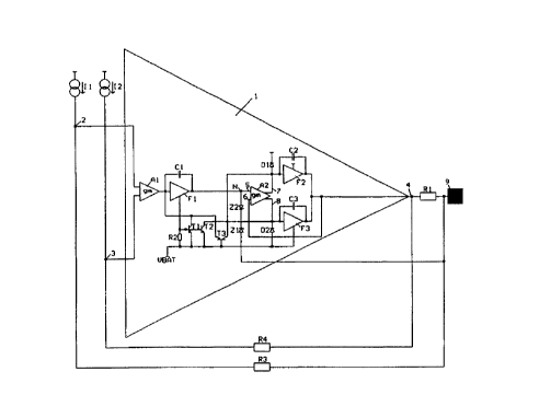
The figure shows a power amplifier known per se, having a protective circuit
in
accordance with the invention. The power amplifier is generally denoted 1 and
has
IO two input terminals 2 and 3, respectively, and one output terminal 4.
In a manner known per se, the power amplifier 1 comprises a transconductance
amplifier A 1 having two input terminals and one output terminal. The input
terminals of the transconductance amplifier A 1 are connected to the input
terminals
IS 2, 3 of the power amplifier I and, thus, constitute, at the same time, the
input
terminals of the power amplifier shown. The output terminal of the trans-
conductance amplifier A 1 is connected to the input terminal of an integrator-
coupled amplifier F 1 between whose input terminal and output terminal, a
compensating capacitor C I is connected.
The output terminal of the amplifier F 1 is connected, via a node N, to a
first input
terminal 5 of a transconductance amplifier A2 whose other input terminal 6 is
connected to the output terminal 4 of the power amplifier 1.
The transconductance amplifier A2 has two output terminals 7 and 8; the output
terminal 7 being connected to the input terminal of an integrator-coupled
amplifier
F2 between whose input terminal and output terminal a compensating capacitor
C2
is connected and whose output terminal is connected to the output ternlinal 4
of the
power amplifier I. The supply voltage terminal of the amplifier F2 is
connected to
ground.
CA 02271709 1999-OS-07
WO 98I21823 3 PCT/SE9'7/01858
In a corresponding manner, the output terminal 8 of the transconductance
amplifier
A2 is connected to the input terniinal of an integrator-coupled amplifier F3
between
whose input terminal and output terminal a compensating capacitor C3 is
connected
and whose output terminal is also connected to the output terminal 4 of the
power
amplifier 1. The supply voltage terminal of the amplifier F3 is connected to a
supply
voltage VBAT.
The components hitherto described as being included in the power amplifier 1,
are
components that are normally included in such an amplifier.
The embodiment of the protective circuit in accordance with the invention,
illustrated on the drawing, comprises a first resistor Rl which is
interconnected
between the output terminal 4 of the power amplifier 1 and a wire connection
terminal 9 via which the line interface circuit, not shown in any detail, is
intended to
feed one wire of a two-wire telephone line (not shown).
To anti-series connected zener diodes Z 1 and Z2 are interconnected between
the
wire connection terminal 9 and the node N, i.e. the interconnection point
between
the output terminal ofthe amplifier F1 and the input terminal 5 of the trans-
conductance amplifier A2.
A resistor R2 is interconnected between the supply voltage terminal of the
amplifier
F I and the supply voltage VBAT. The supply voltage terminal of the amplifier
F 1
is, moreover, connected to the base of two transistors T 1 and T2, whose
emitters are
connected to the supply voltage VBAT.
The collector of the transistor T 1 is connected, on the one hand, to the
input
terminal of the amplifier F 1 and, on the other hand, to the emitter of a
transistor T3 .
The base of the transistor T3 is connected to the supply voltage VBAT and its
collector is connected, on the one hand, to the input terminal of the
amplifier F2
CA 02271709 1999-OS-07
WO 98I21823 4 PCT/SE97/01858
and, on the other hand, to the anode of a diode D 1 whose cathode is connected
to
ground.
The collector of the transistor T2 is connected, on the one hand, to the input
terminal of the amplifier F3 and, on the other hand, to the cathode of a diode
D2
whose anode is connected to the supply voltage VBAT.
In the embodiment shown on the drawing, the input terminals 2 and 3 of the
power
amplifier 1 are connected, on the one hand, to a respective current generator
I1 and
I2, respectively, and, on the other hand, via a respective resistor R3 and R4,
respectively, to the wire connection terminal 9 and the output terminal 4,
respectively, of the power amplifier 1.
In normal operarion, the output current fi om the power amplifier 1 is an
amplified
copy of the difference between the input currents Il and I2. In this
condition, the
voltage on the wire connection terminal 9 is equal to the voltage in the node
N, i. e.
the interconnection point between the output terminal of the amplifier F 1,
the input
terminal 5 of the transconductance amplifier A2 and the anode of the zener
diode
Z2.
At sudden positive or negative changes of the voltage on the wire connection
terminal 9, the voltage in the node N will not change quite as sudden since
the
voltage in the node N is limited by the slew rate of the amplifier F 1.
The voltage difference between the wire connection terminal 9 and the node N
corresponds to the zener voltage of the zener diode Z 1 or Z2. When this
voltage
difference amounts to the zener voltage for the zener diode Z 1 or Z2, also
the
voltage in the node N will be forced to change by voltage changes on the wire
connection terminal 9. Thus, the voltage difference between the wire
connection
terminal 9 and the node N will be kept constant at the zener voltage for Z1 or
Z2,
CA 02271709 1999-05-07
WO 98/21823 5 PCTISE97/01858
whereby the maximum output current of the power amplifier 1 will be limited to
the
zener voltage divided by the resistance of the resistor R1.
If the change of the voltage on the wire connection terminal 9 is larger than
the
zener voltage of the zener diode Z 1 or Z2, thus, also the voltage in the node
N will
be changed by force.
At a quick, positive change of the voltage in the node N, the current through
the
resistor R2 will be so large that the transistor Tl starts to conduct. Hereby,
the
capacitor C 1 across the amplifier F 1 will quickly be recharged to the
voltage
appearing in the node N. In the same manner, the capacitor C3 across the
amplifier
F3 will be recharged through the transistor T2 which also becomes conductive
by
the voltage drop across the resistor R2.
The capacitor C2 across the amplifier F2 will also be recharged through the
diode
D 1, but this is not critical since the amplifier F2 is not active under the
circum-
stances in view of the fact that its supply voltage terminal is connected to
ground.
At a quick, negative change of the voltage in the node N, the capacitor C 1
will
attempt to pull the emitter of the transistor T3 to a voltage below the supply
voltage
VBAT. Hereby, the transistor T3 becomes conductive and the capacitor C 1 is
quickly recharged to the voltage appearing in the node N. The charging current
for
the capacitor C 1 through the transistor T3 is also used to quickly recharge
the
capacitor C2. The capacitor C3 is recharged via the diode D2, but this
recharging is
not critical since the amplifier F3 is not active under the circumstances.
By quickly recharging the compensating capacitors included in the power
amplifier
by means of the protective circuit according to the invention, thus, upon over-
excitation, the maximum output current that can be outputted by the power
3 0 amplifier, on the one hand, and the tim a during which the power amplifier
is over-
excited and outputs the maximum output current, on the other hand, are
limited.
CA 02271709 1999-OS-07
WO 98/21823 PCT/SE97/01858
6
The protective circuit described above for protecting the power amplifier 1
against
sudden positive and negative voltage changes appearing on its output terminal
4. is
according to the invention adapted to quickly recharge the compensating
capacitors
C l, C2, C3 included in the power amplifier 1. By quickly recharging the
capacitors
C 1, C2 and C3, each individual amplifier F l, F2 and F3, respectively, in the
power
amplifier 1 is. thus. protected. Therefore, the protection of the power
amplifier 1 is
based on the protection of the respective amplifier F1, F2 and F3.
Thus. the amplifier F 1 is protected in accordance with what has been stated
above
against sudden. positive voltage changes appearing on its output terminal,
i.e. in the
node N, in that the transistor T 1 becomes conductive and establishes a
current path
to the supply voltage VGAT so that the capacitor C I is quickly recharged.
Against sudden, negative voltage changes appearing on its output terminal, i.
e. in
the node N, the amplifier F 1 is protected in accordance with what has been
stated
above in that the transistor T3 becomes conductive and establishes a current
path via
the diode D 1 to ground so that the capacitor C 1 is recharged.
It should be pointed out that the transistors T 1 and T3, in the general case.
can be
replaced by other switches known per se.
In the embodiment of the power amplifier 1 and the protection circuit
illustrated on
the drawing, both amplifiers F2 and F3 are protected in accordance with what
has
been stated above by recharging the associated capacitor C2 and C3,
respectively,
via a current path established by the diode D 1 to ground and via a current
path
established by the transistor T2 to the supply voltage VBAT, respecrively. In
view
of the fact that the output terminals of the amplifiers F2 and F3 are
interconnected,
the capacitor C2 will thus be recharged at sudden, negative voltage changes.
while
the capacitor C3 will be recharged at sudden, positive voltage changes.