Note: Descriptions are shown in the official language in which they were submitted.
CA 02272560 1999-OS-20
WO 98/24210 ~ PCT/US97/22067
1
CARRIER PHASE SYNCHRONIZATION BY REVERSE PLAYBACK
Technical Field
This invention relates generally to synchronization and demodulation
techniques
' S in digital communication systems where phase locked loops are employed.
More
particularly, this invention relates to demodulation schemes that require
synchronizing
the frequency and/or phase of a local oscillator to a received carrier.
Background Art
Demodulation schemes that employ phase locked loops typically do not have an
internal signal source that is initially synchronized precisely with a
received burst
carrier signal. Thus, receivers use the phase locked loops to converge on an
incoming
frequency and/or phase during the "acquisition" of a received carrier signal.
An
acquisition phase occurs before valid data can be extracted and includes both
carrier
acquisition and symbol synchronization.
The steps of carrier acquisition and symbol synchronization are often
unproductive overhead time in communication systems. In communication systems
conveying lengthy transmissions of large amounts of data, this overhead
acquisition
phase is relatively unimportant. However, in certain other systems, such as
TDMA burst
systems, slow overhead acquisition times translate into unacceptably low
operating
efficiencies.
Various demodulation methods have been used to rapidly extract data from a
carrier signal. As an example, the technique known as "differential"
demodulation is a
robust method of data extraction, but the penalty for using it is a 3-6dB
performance
loss that leads to higher transmission power requirements, greater flux
density,
unsuitable bit error rates, and/or greater liikelihood of interference with
adjacent
channels.
A phase coherent demodulator solves the 3-6dB penalty of differential
demodulation. With coherent demodulation, a phase locked loop accurately
achieves
earner synchronization. The problem with the phase locked loop's ability to
acquire
frequency and phase synchronization is thal: acquisition times are highly
dependent
upon the frequency and phase error, or the amount of deviation between the
incoming
signal and an internal phase locked loop osciillator. Phase locked loops can
require an
CA 02272560 1999-OS-20
WO 98/24210 ~ PCT/US97/22067
2
undesirably long time to converge on a signal during acquisition unless the
loop filter
bandwidth is made very wide. The wider the bandwidth, the more the phase
locked loop
exhibits phase fitter.
An attempt to overcome this problem by estimating phase based upon a captured
block of samples rather than relying solely a phase locked loop has been
developed.
This technique is called Block Phase Estimation. Block Phase Estimation has
one major
limitation. It does not work well if the frequency error is more than
approximately one
percent of the symbol rate. Unfortunately, frequency errors of greater than
one percent
are not uncommon.
One could simply capture an entire burst and reprocess the burst over and over
as
taught in U.S. Patent No 5,440,265 assigned to the assignee of the present
invention.
But excessive reprocessing of symbols leads to transport delay and should be
kept to a
minimum. Moreover, reprocessing a block of symbols in a consistently forward
order
after a phase locked loop has begun its convergence process and has partially
acquired a
frequency and a phase causes the phase locked loop to experience a
discontinuity or
transient that extends the carrier acquisition time. In particular, the phase
of the
incoming signal at the end of the block typically bears no relationship to the
phase of
the incoming signal at the beginning of the block. Thus, phase convergence
efforts of
the phase locked loop in a prior block-processing pass are largely lost when a
subsequent block-processing pass begins.
Disclosure of Invention
Accordingly, it is an advantage of the present invention that improved
synchronization and demodulation techniques for use in digital communication
systems
where phase locked loops are employed are provided.
Another advantage is that the present invention provides rapid carrier
acquisition
and symbol synchronization with minimal transport delays and overhead
processing
time.
Another advantage is that the present invention allows a phase locked loop to
achieve carrier acquisition in response to a signal presented in a reverse
order.
The above and other advantages of the present invention are carried out in one
form by a method for rapid Garner phase synchronization to an incoming signal
conveying data in a stream of symbols. This method includes the steps of
estimating
CA 02272560 1999-OS-20
WO 98/24210 - PCT/US97/22067
3
symbol timing on an incoming block of symbols, sampling the incoming signal in
-
response to the estimated symbol timing to produce samples in a forward order,
buffering the incoming block of samples into a memory, reading the samples
from
memory in a reverse order, and carrier phase synchronizing an oscillator
signal to the
samples read in reverse order from memory.
Brief Description of Drawings
A more complete understanding of the present invention may be derived by
referring to the detailed description and claims when considered in connection
with the
Figures, wherein like reference numbers refer to similar items throughout the
Figures,
and:
FIG. 1 shows a block diagram of a digital communications demodulator
configured in accordance with the present invention;
FIG. 2 shows a flowchart of a carrier phase synchronization by reverse
playback
process;
FIG. 3 shows a timing diagram of an exemplary phase locked loop frequency
error during carrier synchronization; and
FIG. 4 shows a timing diagram of an exemplary phase locked loop phase error
during carrier synchronization.
Best Modes for Carrying Out the Invention
FIGS. 1 through 4 illustrate preferred embodiments of an apparatus and method
of
rapid carrier phase synchronization in a digital communications receiver
demodulator.
Rapid Garner phase synchronization is achievE;d through a technique of reverse
playback
of stored samples into a phase locked loop.
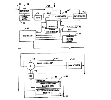
FIG. 1 shows a block diagram of an exemplary digital communications receiver
demodulator 10 which may be implemented with discrete components, with an
integrated circuit, or with the aid of a Digit;il Signal Processor (DSP). FIG.
1 depicts
digital component blocks used for synchronization and demodulation of radio
frequency
signals in a digital communications receiver. In general, the function of
demodulator 10
is to extract digital data from a baseband communication signal and deliver
the data to a
device (not shown) which consumes or otherwise has a use for the data.
Although the
CA 02272560 1999-OS-20
WO 98!24210 - PCTIUS97/22067
4
preferred embodiment works with quadrature signals, the quadrature signals are
not
shown for convenience.
An input terminal 20 of demodulator 10 couples to a first input of an A/D
converter 22 having a first output coupled to a first data input of a
multiplexes (mux)
24. A second input of A/D converter 22 couples to an output of a symbol clock
circuit
26. A second output of A/D converter 22 couples to a data input of a first-
in/first-out
(FIFO) buffer memory 28. A control input of FIFO memory 28 couples to an
output of a
digital controller 30. A second data input of mux 24 couples to the output of
FIFO
memory 28. A selection input of mux 24 is coupled to an output of controller
30. An
output of mux 24 couples to inputs of a bank of interpolators 32, each of
which has an
output coupled to an input of a symbol synchronizer circuit 34 and to a data
input of a
mux 36. A selection input of mux 36 couples to an output of controller 30. The
output
of mux 36 couples to a data input of a forward/reverse readout memory 38. An
address
input of forward/reverse readout memory 38 couples to an output of controller
30. A
second input of symbol synchronizer circuit 34 couples to an output of
controller 30.
The output of the symbol synchronizer circuit 34 also couples to an input of
controller
30. The data output of forward/reverse readout memory 38 couples to a first
input of a
phase comparator 40.
An output of phase comparator 40 couples to an input of a data detector 42. An
output of data detector 42 couples to an input of controller 30 and provides
the data
output from demodulator 10. The output of the phase comparator 40 also couples
to a
signal input of a loop filter 44. An output of loop filter 44 couples to an
input of a
numeric controlled oscillator (NCO) 46. A control input of loop filter 44
couples to an
output of controller 30. An output of numeric controlled oscillator 46 couples
to a
second input of phase comparator 40. Phase comparator 40, loop filter 44 and
numeric
controlled oscillator 46 taken together comprise a phase locked loop 48.
Loop filter 44 is desirably configured using conventional digital filtering
techniques which cause phase locked loop 48 to operate as a second or higher
order
loop. Within loop filter 44 is a group of registers 50 containing filter
coefficients that
determine the loop filter bandwidth, as is conventional in digital filters.
Changing the
values of the filter coe~cients causes the loop filter to exhibit a variable
bandwidth.
Coefficient values are supplied to filter coefficient registers by controller
30 in a
manner which is discussed below. Also within loop filter 44 are state variable
registers
CA 02272560 1999-OS-20
WO 98124210 ~ PCT/US97I22067
52 that store instantaneous frequency and phase describing the state of filter
44. Phase,
and more particularly frequency, values are supplied to instantaneous
frequency and
. phase registers 52 by controller 30.
An incoming radio frequency signal entering demodulator 10 has been converted
5 to baseband before it is presented to A/D converter 22 for sampling. The
preliminary
circuitry that performs this baseband conversion is well known to those
skilled in the art
and is not shown in FIG. 1. Prior to the extraction of useful data from the
incoming
signal, demodulator 10 performs symbol synchronization and carrier
acquisition.
During earner acquisition the difference bcaween the frequency of the incoming
baseband signal 20 and the frequency of a local reference oscillator (i.e.,
NCO 46) is
detected by phase comparator 40, and phase locked loop 48 adjusts this
difference until
it is reduced to zero. Differences in phase betv~reen the incoming signal and
NCO 46 are
processed in a similar manner by phase locked loop 48. Thus, phase locked loop
48
"converges" a local oscillator signal to match ~ui incoming baseband signal.
However, before beginning earner acquisition, the initial task performed by
demodulator 10 is to achieve some degree of symbol synchronization without
regard to
the extraction of usable data. In other words, demodulator 10 performs a non-
data
directed symbol synchronization process that does not rely upon information
obtained
from extracting data from the incoming signal.
A carrier phase synchronization by reverse playback process 54 is shown in a
flowchart as FIG. 2. A task 56 makes a ncrn-data directed symbol timing
estimate.
Referring to FIGs. 1 and 2, during task 56, the baseband analog signal is
converted into
a stream of sampled digital representations by A/D converter 22 under the
control of a
symbol clock 26. In addition, during task 56 mux 24 switches data from A/D
converter
22 directly to interpolators 32.
Initially, the output of A/D converter 22 is gated directly through mux 24 to
interpolators 32 while simultaneously loading; the same signal into FIFO 28.
As will be
appreciated by those skilled in the art, intf;rpolators 32 reproduce a sampled
input
waveshape, but delay it in time by a fixed ~unount. In the preferred
embodiment, the
same waveshape is presented to each interpolator 32 at the same time in a
parallel
fashion, but the output from each interpolator 32 generates samples
corresponding to
the waveshape at a time that is unique for each interpolator 32. Of course,
one of the
interpolators 32 may impose a time delay of zero and be implemented by a
direct signal
CA 02272560 1999-OS-20
WO 98124210 - PCT/US97I22067
6
path. Otherwise, the amounts of delay imposed by interpolators 32 are
distributed
throughout a symbol period.
Symbol synchronizer circuit 34 performs comparisons of the waveshapes obtained
from interpolators 32 to ideal phase states for conveyed data to detect the
one
waveshape having the least error from ideal phase states. Controller 30 then
selects this
one interpolator 32 to drive forward/reverse memory 38 through mux 36.
Controller 30
also then causes FIFO 28 to read out its contents through mux 24. From this
point on in
process 54, all signals from A/D 22 are routed through FIFO 28 and mux 24 to
interpolators 32. In addition, the estimated samples generated by the selected
interpolator 32 are routed through mux 36 to memory 38. In the preferred
embodiment,
memory 38 is a random-access memory capable of both writing and reading at the
symbol rate. In other words, memory 38 can perform a write operation and a
separate
read operation during each symbol period.
At the end of task 56 in synchronization process 54, demodulator 10 has
estimated symbol timing and process 54 begins a task 58. To assist with
carrier
convergence, phase locked loop 48 is introduced into process 54 in task 58 and
subsequent tasks. Phase locked loop 48 converges on the frequency and phase of
an
incoming signal. Controller 30 can vary the operating bandwidth of phase
locked loop
48 by changing the filter coefficients of register 50 in loop filter 44 (see
FIG. 1 ). To
minimize the time required for phase locked loop 52 to converge on the
incoming
signal, loop filter 44 is set to a wide bandwidth during task 58. In this
embodiment a
second order phase locked loop is used, mathematically governed by a loop
filter
equation of the type: f(s) = a( 1 + b/s). The b/s term of the loop filter
equation is a
frequency term having a polarity characterized by the value in instantaneous
frequency
register 52. The value in the instantaneous frequency register 52 corresponds
to the
difference between the current frequency that the numeric controlled
oscillator 46 is
generating and the incoming samples from memory 38.
During task 58 and subsequent tasks, controller 30 causes addresses presented
to
memory 38 to play back samples in a particular order. During task 58, samples
written
into memory 38 are immediately read from memory. This causes the samples to be
played back in a forward order. Task 58 in FIG. 2 shows a forward order pass
using
wide bandwidth. Loop filter coefficients register 50 is loaded with wide
bandwidth
coefficients. The instantaneous frequency register 52 is set to an
initializing value.
CA 02272560 1999-OS-20
WO 98/24210 - PCT/ITS97/22067
7
FIG. 3 shows a timing chart of an exemplary output waveshape of phase locked
loop 48 during the first pass of task 58. At the a;nd of forward pass task 58,
phase locked
loop 48 has converged much closer toward the zero frequency error value than
it was at
the beginning of pass one.
FIG. 4 shows an exemplary phase error waveshape of phase locked loop 48 during
each of three memory playback passes. During the time period of task 58, phase
locked
loop 48 has also been converging toward the zero phase error value, as shown
in FIG. 4.
However, only a small amount of phase convergence has occurred, due in part to
the
wide bandwidth of loop filter 44 during task 58.
Controller 30 reverses the polarity of instantaneous frequency register 52 at
the
beginning of a task 60 in preparation for a backward readout from memory 3 8.
The
filter coefficients register is set to narrow bandwidth for finer phase
convergence, which
also reduces phase "fitter" in the phase locked loop.
If phase locked loop 48 were presented with another identical forward readout
of
I S the samples from memory 38 after the forward pass of task 58, benefits
gained toward
phase convergence during task 58 would be lost. Unlike frequency, the phase of
the
incoming signal at the end of task 58 typically bears no relation to the
initial phase of
the input signal. However, by reversing the direction of the samples presented
to phase
locked loop 48 at this juncture and reversing the polarity of the frequency
state variable
of loop filter 44 to accommodate the simulated backward motion in time, the
phase
convergence gained during task 58 is preserved.
Task 60 of process 54 is a reverse order pass using a narrow bandwidth in loop
filter 44 and an inverted polarity for the freduency state variable value in
register 52
(see FIG. 1 ). The same samples presented to phase locked loop 48 during task
58 are
presented again in task 60, except in reverse order. Controller 30 causes
forward/reverse
memory 3 8 to readout in a reverse (back to i:ront) order during task 60. With
task 60,
controller 30 sets loop filter coefficients register 50 so that phase locked
loop 48
exhibits a narrow bandwidth. Phase locked loop 48 continues toward convergence
at the
point where it left off at the end of task ~~8. The dotted line 62 shown in
FIG. 4
represents the sample block readout as if it were flowing backward in time.
The solid
line shown in the second pass of FIG. 4 shows the same waveform mirrored in
the
forward direction to indicate the phase convergence proceeding forward in
time. During
task 60 no incoming data is lost, since new incoming data is being written
into
CA 02272560 1999-OS-20
WO 98124210 ~ PCT/US97/22067
8
forward/reverse memory 3 8 at the same time the prior data block samples are
being read
in reverse order.
Also during task 60, controller 30 searches for a special data pattern or
preamble
signifying the beginning of the incoming signal. When the beginning of the
incoming
signal has been detected, for example at a point 63, controller 30 can reverse
direction
of the readout from memory 38 immediately and continue to extract valid data.
At this
point, phase locked loop 48 has nearly achieved a precise carrier
synchronization.
After task 60, a task 66 is performed continuing to use a narrow bandwidth in
loop filter 44 in the preferred embodiment of this invention. In alternate
embodiments,
filter coefficients 50 could be progressively adjusted for increasingly
narrower
bandwidth during the third pass of task 66. In addition, the polarity of
frequency state
variable 52 in the loop filter 44 is inverted from its state at the end of
task 60. FIG. 4
shows the waveshape converging on the zero phase error Iine at the end of task
66.
Beginning in task 66, demodulator 10 has achieved sufficiently precise carrier
frequency and phase synchronization, that data detector 42 can extract valid
data for the
data consumer. Desirably, demodulator 10 can now continue to perform normal
data
extraction on incoming signals or perform other tasks required by controller
30. The
length of the processed block of samples is desirably no longer than needed to
minimize
transport delay. This block length is determined by worst case frequency
offset and
signal-to-noise ratio and varies according to the application.
In summary, the present invention provides a rapid carrier synchronization
apparatus and method. The present invention acquires symbol timing rapidly by
storing
incoming samples into a forwardlreverse readout memory and using a phase
locked
loop during reverse readout to converge on the phase of stored samples while
making
use of phase convergence attained during a prior pass.
Although the preferred embodiments of the invention have been illustrated and
described in detail, it will be readily apparent to those skilled in the art
that various
modifications may be made therein without departing from the spirit of the
invention or
from the scope of the appended claims.