Note: Descriptions are shown in the official language in which they were submitted.
CA 02272619 1999-05-21
V1V0 99I18646 PCTIUS98/17404
-1-
Description
MODULATION COMPENSATED CLAMP CIRCUIT
TECHNICAL FIELD
The present invention generally relates to
radio frequency identification ("RFID") devices, and more
particularly to an RFID for close proximity operation.
BACKGROUND ART
Remote electronic identification devices typi-
cally consist of remotely disposed transponders and an
interrogator unit. The operating range of such devices
depends on the underlying architecture of the transponder
unit. In U.S. Patent No. 4,333,072 to Beigel, for exam-
ple, a remote identification system consists of a probe
circuit (interrogator) operating in close proximity to an
implant circuit (transponder). The implant circuit is
powered when the probe circuit is brought close to the
implant, producing a voltage by induction across a coil
in the implant. Information from the implant is trans-
ferred to the probe by varying the inductive load on the
implant's coil and detecting such variations in the
probe. This mode of operation requires that the probe be
very closely spaced from the implant, thus greatly limit-
ing the range of operation of such devices.
Other remote identification systems use radio
frequency signaling to provide the communication lank
between interrogator and transponder. In one class of
these radio frequency identification (RFID) devices, the
RF signal includes a power signal that is transmitted to
the transponder device. This power signal charges up a
power supply capacitor in the transponder, which serves
as the power source for the transponder. The transmis-
sion of data from the transponder involves the generation
and transmission of radio frequency energy. The power
supply capacitor must be of sufficient size to provide
adequate power for such transmissions. Such transponders
*rB
__.._. __._
CA 02272619 1999-OS-21
WO 99I18646 PCTIUS98/17404
-2-
allow reading distances on the order of 2 meters. This
type of transponder, however, is not practical in appli-
cations requiring small size: e.g. livestock identifica-
tion by subcutaneous implantation of the device.
In a third category of RFIDs, an alternative
approach combines features from the above two designs.
An interrogator transmits an RF signal which includes a
power signal. The voltage induced across the transponder
coil by the received power signal is sufficient to oper-
ate the transponder circuitry, but not sufficient to
generate its own radio signal. A capacitor coupled in
parallel with the coil forms a tank circuit, whose Q is
varied by varying a resistive load placed across the tank
circuit. This changes the tuning of the tank circuit,
resulting in variations in the reflected signal which can
be detected by the interrogator. Thus, the transponder
is able to convey its data to the interrogator simply by
modulating the resistive load accordingly and allowing
the interrogator to detect variations in the reflected
signal.
An overvoltage circuit is typically employed to
protect the device against overvoltage conditions. Prior
art solutions include the use of a zener diode which has
a breakdown voltage at a level above which the voltage
would be detrimental to the transponder. The diode is
coupled between the pins of the transponder coil. The
presence of an overvoltage condition across the coil
causes the zener diode to conduct, thus driving V~ to
ground and effectively turning off the device. U.S.
Patent No. 5,479,172 discloses another approach wherein
is compared against a reference voltage and a shunting
transistor is turned on to shunt the current from a rec-
tifier to ground, thus limiting V~ to the reference
voltage.
A problem arises when the interrogator operates
at close range. The strong signal from the interrogator
causes the overvoltage circuit in the transponder to
conduct. The current into the tank circuit, therefore,
CA 02272619 1999-OS-21
VVO 99/18646 PCTIUS98117404
-3-
is affected both by operation of the overvoltage circuit
and the modulated resistive load. When the transponder
attempts to transmit data by varying the load resistance,
which varies the current into the tank circuit, such
variations in the current become masked by the operation
of the overvoltage circuit.
The circuitry shown in Fig. 3 is typical of
prior art transponders and illustrates how this masking
effect comes about. A modulation signal varies the con-
ductivity (resistance) of transistor R, thus changing the
tuning of the tank circuit L/C, in accordance with data
stored in the transponder. An overvoltage circuit 22
includes a comparator 21 and a shunt 23. When the
overvoltage circuit 22 is turned on, there is no way to
tell whether the current change is due to an overvoltage
condition or to the modulation of transistor R. What can
happen is that when the modulator turns on transistor R,
current that might have flowed through the overvoltage
shunt 23 will flow through transistor R instead. The
overall magnitude of the current flow has not changed and
so there is no change in the Q of the tank circuit.
Since the Q (and thus the tuning) remains unchanged,
there is no change in the reflected signal for the inter-
rogator to detect, and thus no data transmission.
It is therefore desirable to have a transponder
which can operate in close proximity to the interrogator,
and thus exhibit a wide range of operating distances.
What is needed is a transponder that is not affected by
operation of an overvoltage circuit which is likely to
turn on due to the strong signal received from a closely
positioned interrogator.
SU1~IARY OF THE INVENTION
In accordance with the present invention, a
radio frequency identification (RFID) tag comprises a
tank circuit for receiving a power signal transmitted on
a radio frequency (RF) carrier by a remote interrogator
unit. Information is conveyed from the tag to the inter-
CA 02272619 1999-OS-21
WO 99I18646 PCT/US98I17404
-4 -
rogator by varying a resistive load placed across the
tank circuit as a function of data read from memory.
Corresponding variations in the reflected signals are
then detected by the interrogator.
A voltage clamp provides overvoltage protec-
tion. Triggering of the clamp is produced by modulation
in accordance with the data. The clamp includes a shunt-
ing means which operates in conjunction with a modulation
circuit so that data transmission is possible even during
an overvoltage condition.
BRIEF DESCRIPTION OF THE DRAWINGS
Fig. 1 shows a block diagram of the RFTD tag in
accordance with the present invention.
Fig. 2 illustrates the modulation circuit of
the present invention.
Fig. 3 shows a prior art modulation scheme.
BEST MODE FOR CARRYING OUT THE INVENTION
Referring to Fig. 1, a radio frequency identi-
fication (RFID) system 100 includes an interrogator unit
102 and a transducer unit (tag) 104. The interrogator
l02 includes a transmit coil 103 for transmitting an RF
signal to the tag 104.
The tag 104 comprises a pick-up coil ht, which
together with capacitor Ct, forms a tank circuit 120.
Coupled across the tank circuit are a voltage clamp I22,
a load modulation circuit 124, and a full-wave bridge
rectifier 126. The voltage clamp 122 is an overvoltage
protection device which limits the maximum voltage devel-
oped across the tank circuit 120. In such devices, the
voltage across coil Lt can increase to a level that is
quite high, especially when the load is low and the Q of
the tank circuit is high. Such high voltages are likely
to cause failure of the device electronics. When the
voltage across the coil nears the upper limit of the
device, clamp 122 switches on to increase the current
CA 02272619 1999-OS-21
Vw0 99I18646 PCT/US98/17404
-5-
across the clamp and thus reduce the voltage to a safer
level.
The modulation circuit 124, varies the loading
across tank circuit 120, which in turn varies the Q fac-
for of the tank circuit. The modulation circuit operates
under the control of a controller 134 which varies the Q
of tank circuit 120 in correspondence with the data to be
conveyed to the interrogator Z02. Varying the Q alters
the reflected signal. Thus, the data is "transmitted" as
the interrogator detects corresponding changes in the
reflected signal.
The bridge rectifier l26 charges a small supply
capacitor Cf to provide the supply voltage V~ needed by
the tag. The supply voltage provides power to a nonvola-
tile memory 132, which includes a voltage pump to provide
a programming voltage V~. In addition to providing
internal power to the transducer 104, the bridge circuit
126 also provides a clock signal, based on the incoming
signal from the interrogator 102, to a clock generator
136.
The memory 132 is a 256-bit EEPROM, consisting
of eight 32-bit pages. Page 0 is organized as a 24 bit
datum plus eight write-lock bits. Pages 1 - 7 are user
pages. The write-lock bits determine whether the corre-
sponding 32-bit page can be written. Password protection
is available. The password is stored in user page 7.
Read and write access to the memory 132 are provided
through controller 134. A demodulator 138 demodulates an
incoming data signal and feeds the data into the control-
ler l34 which then writes it to memory 132. The data
signal includes a sequence of command bits followed by an
optional sequence of data bits.
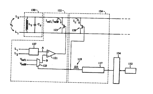
Turning to Fig. 2, the modulation circuit 124
comprises an encader/modulator 117 which drives the gate
of a load transistor 129. The drain and source of the
load transistor 129 are coupled across the terminals of
tank circuit 120. The output pulses comprising a modula-
tion signal 119 of encoder/modulator 117 modulate load
CA 02272619 1999-OS-21
WO 99/18646 PCT/US98I17404
-6-
transistor 129, turning the transistor on and off. As
load transistor 129 alternates between conduction and
nonconduction, the Q of the tank circuit 120 (i.e. its
tuning) varies correspondingly. The encoder/modulator
117 is capable of a variety of well-known encoding
schemes, including Manchester (bi-phase), Miller, differ-
ential bi-phase, and modified differential bi-phase en-
coding. The encoded signals can then be further modu-
lated by phase shift keying or frequency shift keying.
In accordance with the present invention, the
voltage clamp 122 comprises a shunt transistor 123 having
a source-drain connection across tank circuit 120. An
output of comparator 121 drives the gate of shunt tran-
sistor 123.
A detector 127 detects the potential difference
V~ across the coil Lt which is fed into a first input A of
the comparator. A voltage selector 125 switches one of
two reference voltages V~ef~ and V~ef2 into a second input B
of comparator 121. The modulation signal 119 feeds into
selector 125 to switch between V,.ef1 and ~l~ef2~ den the
voltage on the A input exceeds the voltage on the B in-
put, comparator 121 outputs a voltage greater than the
threshold voltage Vt of shunt transistor 123, turning on
the shunt resistor. When the voltage on input A is less
than the voltage on the B input, comparator 121 outputs a
voltage less than Vt which will maintain shunt transistor
123 in the off condition.
Still referring to Fig. 2, the modulation cir-
cuit 124 and voltage clamp circuit 122 cooperate in the
following manner. Controller 134 reads memory 132 and
produces a corresponding series of pulses 119 represent-
ing the 1's and 0's of the data via modulator 1I7. As-
sume that a '1' pulse turns on load transistor 129 and
that a '0' pulse turns it off. Thus, for a '1' bit, the
load transistor is turned on, resulting in a load current
I~ which "bleeds" current from the tank circuit 120 and
decreases its Q. Conversely, for a '0' bit, the load
CA 02272619 1999-OS-21
WO 99I18646 PCTIUS98/17404
-7-
transistor is off, thus eliminating the loading on the
tank circuit and increasing its Q.
This is the typical operation of the tag during
a non-overvoltage condition. Recall, however, that the
pulses l19 also drive selector l25 whose output feeds
into comparator 121. For discussion purposes, assume
that a '1' pulse selects V~ef~ and a '0' pulse selects
VrefO ~ and that V,.eft is greater than V~efO' In the
non-overvoltage condition, the coil voltage V~ will be
less than both V~ef1 and VrefO~ The output of comparator
121, therefore, will be negative (i.e. less than Vt of
shunt transistor 123) and thus shunt transistor will
remain non-conductive.
Consider next an overvoltage condition where
the potential V~ across coil Lt becomes equal to or
greater than the upper voltage limit V~~m of the tag,
above which damage to the device is likely to occur.
For each occurrence of a '1' bit during an
overvoltage condition, the load transistor 129 is turned
on as described above, causing load current I~ to flow out
of the tank. In addition, V~ef~ is switched into
comparator 121 whose output is (V~ - V,.ef>> ~ properly
selecting V~ and V,.ert will turn shunt transistor 123 on by
a certain amount to draw additional current I~ef~ out of
tank circuit 120. This will have the effect of lowering
the Q as in the non-overvoltage case. In the overvoltage
case, however, the Q is even lower because of the addi-
tional load current I~ef~. The additional load current
I~f~ has the further effect of lowering the coil voltage
V~ to a value below V~~m, thus alleviating the overvoltage
condition.
For each occurrence of a '0' bit during an
overvoltage condition, the load transistor 129 remains
off as in the case of the non-overvoltage condition. V~efO
is switched into comparator 121. The output of
comparator 121 is (V~ - V~efO~ ~ properly selecting V~ and
Vrefo w111 cause shunt transistor 123 to draw current I~efo
out of the tank circuit. However, since V~efO iS less than
CA 02272619 1999-OS-21
1~0 99/18646 PCTIUS98117404
_g_
V~ef~, the comparator will drive the gate of shunt transis-
for 123 at a higher voltage, causing a higher current
flow I,.efo through the shunt transistor. Thus although
load transistor 129 is off for a '0' bit, shunt transis-
for 123 is on. V~efo l.s Set so that load current I,.eto
alone is sufficient to lower the coil voltage V~ to a
value just below V~~m to alleviate the overvoltage condi-
tion.
Suppose in the case of a '0' bit, where the
load current is I~efO ~ the resulting Q is Qo; and that in
the case of a '1' bit, where the total load current expe-
rienced by tank circuit 120 is I~ + I~ef~, the resulting Q
is Q~. So long as Qo and Q~ are sufficiently separate, a
'0' bit can be distinguished from a '1' bit. Thus, it
can be seen that by properly selecting V~efl and V~,efo the
tuning of the tank circuit can be varied sufficiently so
as to change the signal reflected by the tag enough to
distinguish between a '0' bit and a '1' bit. At the same
time, the overvoltage condition is avoided (by virtue of
the shunting currents I~efi, I~efo) without masking the
signal carrying the data contained in the tag.