Note: Descriptions are shown in the official language in which they were submitted.
WO 98/31049 PCT/US97/I9533
to
LASER BASED METHOD AND SYSTEM
FOR INTEGRATED CIRCUIT REPAIR OR RECONFIGURATION
Technical Field
The present _ inuen' an.~ ~N~ fates to laser methods
and systems for memozy anCt ibgi~: integrated circuit
production and repair and, in particular, to creating
unique patterns on an etch protection top layer material
in response to reconfiguration data unique to each
integrated circuit.
Backcrround of the Invention
IC (integrated circuit) device fabrication on
semiconductor wafers, which is presented herein only by
way of example to processing and the manufacture of logic
products and memory devices such as DRAMS, SRAMs, and
embedded memories that contain electrically conductive
links, typically employs photoresist layering and
patterning to identify areas of the IC device for
subsequent processing such as doping or removal.
Photoresist materials are etch resistant and protect
covered areas of the IC device from at least one
subsequent processing step.
Photolithography is a typical wafer patterning
process that employs photoresist materials sensitive to
certain wavelengths of light that traditionally match the
emission wavelengths of the lines of a mercury lamp such
as G (436 nm), H (408 nm), or I (365 nm) or the emission
wavelengths of excimer lasers such as ArF (193 nm) and KrF
CA 02272653 1999-os-Zi SUBSTITUTE SHEET (RULE 26)
WO 98/31049 PCT/US97/19533
2
(248 nm). Conventional photoresist materials generally
comprise positive photoresists that become soluble where
exposed to light and negative photoresists that become
polymerized (insoluble) where exposed to light.
In photolithography, a required pattern is first
formed in expensive reticles or photomasks and then
transferred into a resist layer of a wafer. Lamp sources
and, more recently, certain types of laser systems have
been employed for simultaneously exposing the resist layer
of every IC device on a wafer to a reverse image of the
photomask. Photolithography is, therefore, especially
suited for batch fabrication of repeatable features on IC
devices. Photolithography and other VLSI (very large
scale integration) memory fabrication processes are
described in detail in Handbook of Microlithoaraphy.
Micromachinina, and Microfabrication: Volume 1:
Microlithoaraphy, Edited by
P. Rai-Choudbury, SPIE Volume PM39 and VLSI Fabrication
Principles: Silicon and Gallium Arsenide, by Sorab K.
Ghandi, 1994, ~ John Wiley & Sons, Inc.
The yield of an IC memory fabrication process is
affected by a variety of factors. Some defects result
from alignment variations of subsurface layers or
patterns, and other defects result from particulate
contaminants and defects in the silicon substrate. Figs.
1, 2A, and 2B show repetitive electronic circuits 10 of an
IC device 12 (Fig. 6) that are commonly fabricated to
include multiple iterations of redundant circuit elements
14, such as spare rows 16 and columns 18 of memory cells
20. With reference to Figs. 2A and 2B, circuits 10 are
also designed to include particular circuit links 22 that
can be removed to disconnect a defective memory cell 20,
for example, and substitute a replacement redundant cell
24. Links 22 are designed with conventional Link widths
25 (about 2.5 ~,m), link lengths 26, and element-to-element
pitches (center-to-center spacings) 28 of about 8 ~.m from
CA 02272653 1999-os-Zi SUBSTITUTE SHEET (RULE 26)
__... ~_
WO 98/31049 PCT/US97/19533
3
adjacent circuit structures or elements 30, such as link
struc-tures 38. Circuits 10, circuit elements 14, or cells
20 are tested for defects, the locations of which may be
mapped into a database or program. Because the defects
are unique from wafer 32 (Fig. 6) to wafer 32 and IC
device 12 to IC device 12, the repair process cannot be
accomplished with conventional photolithographic processes
that employ fixed patterned photomasks.
However, certain lasers can precisely deliver
laser pulses 34 having a laser spot 36 that is big enough
to envelop and "blow" link 22 but generally small enough
to avoid adjacent circuit elements 30. The early physics
and computer modeling for laser-based link blowing are
described by L.M. Scarfone and J.D. Chlipala, "Computer
Simulation of Target Link Explosion in Programmable
Redundancy for Silicon Memory," Journal of Materials
Research, Vol. 1, No. 2, Mar.-Apr. 1986, at 368-81, and
J.D. Chlipala, L.M. Scarfone, and Chih-Yuan Lu, "Computer-
Simulated Explosion of Poly-Silicide Links in Laser-
Programmable Redundancy for VLSI Memory Repair," IEEE
Transactions on Electron Devices, Vol. 36, No. 6, June
1989, at 1056-61. Laser link blowing is now well-refined
and is the method of choice for disconnecting links. The
most prevalent link materials are polysilicon and like
compositions, which respond well to conventional 1.047 ~,m
or 1.064 ~Cm laser wavelengths. Fig. 2C shows a
conventional link structure 38 of Fig. 2A after a
passivation layer 40 and link 22 have been removed by
conventional laser pulses) 34 of prior art energy
distribution.
The technology trend is, however, toward
developing more complex, higher density circuits 10 or
memories having more layers and smaller link structures 38
and memory cell dimensions. As polysilicon links 22
become smaller and more deeply buried, they become more
difficult to sever at the conventional laser outputs and
CA 02272653 1999-os-Zi SUBSTITUTE SHEET (RULE 26)
CA 02272653 2003-05-29
71073-94
4
spot size limitations of 1.047 ~,m or 1.064 ~.m radiation.
Expensive and time-consuming processes are often required to
delicately etch away passivation layers 40 or other surface
layers to make links 22 accessible for subsequent laser
severing.
Another impediment to higher density circuits 10 or
embedded memories is that the electrical resistance of the
conventional polysilicon-like link materials, including
polycide and disilicide, increases as dimensions shrink and
thereby restricts the operating speed of memory cells 20. To
address signal propagation delay associated with the higher
electrical resistance attributed to polysilicon-like links 22,
memory manufacturers have adopted a variety of more conductive
metallic link structure materials such as aluminum, titanium,
nickel, copper, tungsten, platinum, metal alloys, metal
nitrides, cesium silicide, chromide, doped polysilicon,
disilicide gold, nickel chromide, polycide, tantalum nitride,
and titanium nitride, or other metal-like materials.
Another motivation for using metallic links 22 for
redundancy repairing is that these metallic links 22 are often
located closer to the top of the multi-layer structure of the
memory device, thus links 22 are easier for the laser beam to
access without the need of etching out windows within multiple
covering layers. However, many of these materials are more
difficult to process using the 1.047 ~Cm or 1.064 um
wavelengths of conventional link processing laser systems
because these materials have higher optical reflectivities or
higher melting or vaporization points than polysilicon.
Generally, laser severing of these metals creates slag and
debris that surround the crater and cause a lower open
resistance across the severed links 22 and perhaps a circuit
f ai lure .
Higher power laser output is required to process
the metallic link materials and to eliminate potential debris.
However, increasing the laser output power level has
deleterious effects on silicon, gallium arsenide, and
WO 98/31049 PCT/LTS97/19533
other semiconductor substrates 44, other layers 42, and
adjacent circuit structures 30.
Alternatively, in U.S. Patent No. 5,265,114, Sun
et al. employ wavelengths, such as 1.3 Vim, that exploit
5 the absorption contrast between a target such as a metal
link, and a substrate 44, such as silicon. Among other
advantages, the method allows the use of higher energy
laser pulses to sever links 22 without affecting the
silicon substrate 44 and thus creates a greater laser
energy processing window than that allowed by conventional
1.047 ~Cm and 1.064 ~.m laser wavelengths. The open
resistance across links 22 processed by this method is
much higher than the resistance across links 22 severed by
the conventional beams.
As links 22 and pitches 28 become smaller, spot
size limitations become more critical. The selection of
optical elements and their clearance from substrate 44
influence the practical spot-size limits of link-blowing
laser pulses 34. For example, optical elements are
generally maintained at least 10 mm above a link structure
38 to avoid contact with slag or other debris that may
result from link-blowing. The conventional spot size
limit for a link-blowing laser output pulse can be
conveniently approximated as twice the wavelength (2~?.
Thus, for 1.32, 1.06, and 1.04 ~,m-emission materials, the
practical spot size limits for material removal are
roughly 2.64 ~,m, 2.12 ~,m, and 2.08 ~.m, respectively.
Skilled persons will appreciate that shorter
wavelengths, such as 0.532 ~.m, 0.355 ~.m, or 0.266 ~,m,
could be employed to reduce the smallest focused laser
beam spot size for material removal. However, skilled
persons will also appreciate that silicon substrates 44
will strongly absorb wavelengths shorter than about 1 ~.m
such that these wavelengths will inevitably damage
substrates 44, especially at the high power needed for
link blowing.
ca o22~26s3 1999-os-Zi SUBSTITUTE SHEET (RULE 26)
oi~n-eiie:-8890031=KETLEY %0049-8934?O10=BOEHMERT /99-02-12-08:32;001-006 --"
i-ooa r,uo/10 F-Q89
From:FORRESTER & BOEHMER':'
PDX111890.1 26860-0a33:42 PCZ
The smallest focused laser spot 36 currently used
in the industry for repairing 64 megabit DRAMS is about a
2.0 urn dinmeter 96 of laser $pot 36. This spot size is
expected t-.o be useful through 256 megabit and some 1 gigabit
DR.~M desiclns. Fig. 3 is a graph of spot size versus year
demonscrai:ing industry demands for smaller spot, sizes as
link pitc)~ 28 and link ~ridth 25 decrease. The graph is
based on s simple formula fat approximating spot size
demands: spot size = 2 (minimum link pitch) - tsyatem
to accuracy) - 0.5 (link width). The graph assumes D.5 ~cm
accuracy through the year 1s9~, 0.35 ~m accuracy through the
year 1999, and o.25 ~cm accuracy thereafter. Accordingly,
industry experts predict chat spot sizes under 2 ~m will
soon be desirable for processing links 22.
S_ummarv of the Invea
An object of the present invention is, therefore,
to provide an alternative method and system for processing
targets, such as links.
Accordingly, the present invention provides a
system ad method for first exposing or ablating an etch
protecti~sn top layer target material, such as a resist
material or other protective coating, with individually
directed laser output pulses at respective multiple random
target l.~cations on one or more IC devices and then etching
the ands dying targets.
In one embodiment of the present invention, a
target material on a work piece is coated with a layer of
photoresist material. The laser output wavelength is
selected to expose, i.e. activate, the photoresist material.
3d Position data then direct individual laser output pulses
toward negpective multiple positions on the photoresist
material.. Because photoresist exposure requires lees laser
energy ~.han direct link blowing by a laser beam, shorter
wavelength lasers can be employed to expose the photoresist
above a link 22 that needs to be disconnected without the
risk of damage to the substrate or other
AMENC~O SHEET
CA 02272653 1999-OS-21
CA 02272653 2000-04-14
' 71073-94
7
circuit elements. Finally the IC device is developed to remove
the photoresist, and conventional etching techniques are used
to remove the uncovered target or link 22.
In addition to a spot size advantage obtained by
using a shorter wavelength, the lower power of the exposure
process allows the optical elements to be brought closer to the
target and facilitates the practical laser output spot size
factor to be approximately as little as one times the
wavelength.
Alternatively, an etch protection layer such as
resist or other protective coating material can be directly
ablated using a slightly higher, but still relatively low,
power laser. For example, a low power UV laser can be used to
ablate a nonphotosensitve resist material having a low ablation
1.5 threshold. The developing step eliminated, and any ablation-
related debris disappears when the target is etched or when the
rest of the protective layer is removed.
By etching the uncovered links 22 instead of blowing
them, IC device manufacturers can utilize smaller spot sized
and can, therefore, design smaller link lengths 26, link widths
25, and pitches 28, as well as avoid low open resistance across
the severed links 22 and other problems associated with slag
creation. In addition to providing cleaner link removal than
is possible by link blowing, the present invention permits much
greater laser processing windows than is permitted by link
blowing.
In accordance with the present invention, there is
provided a method of selectively removing target material (92)
embedded in a semiconductor device (12), the target material
(92) supported at different locations (106) on a substrate (44)
and covered by at least an etch protection layer (90),
CA 02272653 2000-04-14
71073-94
7a
comprising: providing to a beam positioner (160) beam
positioning data representing locations (106) of the target
material (92) embedded in the semiconductor device (12);
generating, from a laser (120), laser output pulses (94) at a
wavelength shorter than 500 nm and having an energy density of
less than or equal to 50 mJ/cmz; and directing, in response to
the beam positioning data, the laser outputs (94) having a
wavelength of lees than 500nm to impinge the etch protection
layer (90) at positions (150) that are spatially aligned
depthwise with th.e respective locations (106) of the target
material (92), each of the positions (150) being impinged with
at least one separate laser output (94) not directed at another
position (150), and each laser output (94) having spatial
dimensions (98) defining a region (100) of the etch protection
layer (90) that is to be removed, the region (100) having a
spatial spot size diameter (98) of less that 2 Eun, the etch
protection layer (90) including a photoresist material (90),
and each laser output (94) having an energy density sufficient
to activate the region (100) of the etch protection layer (90)
spatially aligned with the position (150) and insufficient to
remove the region (100) of the etch protection layer (90)
spatially aligned with the position (150).
In accordance with the present invention, there is
further provided a laser system (120) for point-to-point
2.'~ exposure of positions (150) on one or more etch protection
layers (90) covering etch targets (92) on a semiconductor chip,
comprising: a beam positioner (160) for directing sequential
laser output pulses (94) in response to position data
determined from characteristics specific to the chip in which
there are randomly located etch targets (92) positioned under
an etch protection layer (90) that includes a photoresist (90),
the position data indicating sequential positions (150) of the
CA 02272653 2000-04-14
71073-94
7b
etch targets (92); an optical component, positionable to be in
proximity to the etch protection layer (90) during laser output
pulse generation, for focusing a laser output toward the
sequential positions (150) to impinge a portion of the etch
protection layer (90) spatially aligned with each position
(150); and a solid-state laser (124) positioned within a laser
resonator (122) for sequentially generating, at a wavelength of
less than 500 nm and at a repetition rate of greater than 300
Hz, the laser output pulses (94) having an energy density less
than 50 mJ/cm2 and sufficient to activate the etch protection
layer (90) at each position (150) but insufficient to ablate
the etch targets (92) and insufficient to completely ablate the
region (100) of the etch protection layer (90) spatially
aligned with the positions (150).
In accordance with the present invention, there is
further provided a method employing on-the-fly laser output
pulses (74) to process positions (150) on an etch protection
layer (70) covering respective links (72) lying spatially below
the etch protection layer (70) and in proximity to a substrate
(44) that is susceptible to damage from the laser output pulses
(74), comprising: providing a beam positioner (160) beam
positioning data representing locations (62) of the links (72)
to be processed, the links (72) lying within about 2 ~m of an
adjacent circuit structure (30); generating solid-state laser
output pulses (74) at a wavelength shorter than or equal to 349
nm and a repetition rate of greater than 300 Hz; and impinging,
with the laser output pulses (74), regions (80) of the etch
protection layer (70) that are spatially aligned with the
locations (62) of the links (72) such that each region (80) is
impinged by a separate laser output pulse (74) having a spatial
spot size (58) of a diameter of less than 1 ~m and
characterized by an energy distribution of less than or equal
CA 02272653 2000-04-14
71073-94
7c
to 50 mJ/cm2 that: is sufficient to ablate the region (80) of
the etch protection layer (70) and expose a portion of the link
(72) but insufficient to blow the link (72) or damage the
substrate (44).
Additional objects and advantages of invention will
be apparent from the following detailed description of
preferred embodiments thereof, which proceeds with reference to
the accompanying drawings.
WO 98/31049 PCT/US97/19533
8
Brief Description of the Drawings
Fig. 1 is a schematic diagram of a portion of a
DRAM showing the redundant layout of and programmable
links in a spare row of generic circuit cells.
Fig. 2A is a fragmentary cross-sectional side
view of a conventional, large semiconductor link structure
receiving a laser pulse characterized by a prior art pulse
parameters.
Fig. 2B is a fragmentary top view of the link
structure and the laser pulse of Fig. 2A, together with an
adjacent circuit structure.
Fig. 2C is a fragmentary cross-sectional side
view of the link structure of Fig. 2B after the link is
removed by the prior art laser pulse.
Fig. 3 is a graph of spot size versus year
predicting the laser spot sizes that will be needed over
time for link processing.
Fig. 4A is a fragmentary cross-sectional side
view of a photoresist-covered, very narrow target
structure receiving a laser pulse characterized by laser
pulse parameters in accordance with the present invention.
Fig. 4B is a fragmentary cross-sectional side
view of the target structure of Fig. 4A with dashed lines
enclosing a laser-activated portion of the photoresist
layer.
Fig. 4C is a fragmentary cross-sectional side
view of the target structure of Fig. 4B subsequent to a
developing step.
Fig. 4D is a fragmentary cross-sectional side
view of the target structure of Fig. 4C subsequent to at
least one etch processing step.
Fig. 5A is a fragmentary cross-sectional side
view of a target structure, covered by a protective layer,
receiving a laser pulse characterized by laser pulse
parameters in accordance with the present invention.
CA 02272653 1999-os-Zi SUgSTiTUTE SHEET (RULE 26)
_ .. _.______ T. ._. . _. _.___ _.____._
CA 02272653 2003-05-29
71073-94
9
Fig. 5B is a fragmentary cross-sectional side view
of the target structure of Fig. 5A subsequent to a laser
ablation processing step.
Fig. 5C is a fragmentary cross-sectional side view
of the target structure of Fig. 5B subsequent to at least one
etch processing step.
Fig. 6 is a partly schematic, simplified diagram of
one embodiment of a laser system incorporating the present
invention.
Detailed Description of Preferred Embodiments
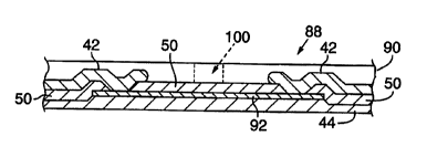
Figs. 4A, 4B, 4C, and 4D (collectively Fig. 4) are
fragmentary cross-sectional side views of a target structure
88 undergoing sequential stages of target processing in
accordance with the present invention. With reference to
Fig. 4, target structure 88 includes an etch-~ target or link 92
that may comprise metal or any other etch-sensitive target
material. Target structure 88 can have much smaller features
and dimensions than those blown by conventional link-blowing
laser pulses 34, i.e. link length 85 and link width (not
shown) can be designed to be smaller than those of links blown
by conventional link-blowing laser pulses 34. Similarly, the
pitch between links 92 can be substantially smaller than the
pitch between links blown by conventional link blowing laser
pulses 34. For convenience, certain features of target
structure 88 that correspond to features of link structure 38
of Fig. 2A have been designated with the same reference
numbers.
With respect to Fig. 4, link 92 is positioned below
an etch protection top layer 90 of a positive photoresist
material. Photoresist layer 90 may be a remnant from a prior
lithographic or other circuit fabrication process or may be
newly applied. Photoresist materials include, but are not
limited to, NovolakT" (M-Cresol formaldehyde) or etch-resistant
poly coatings such as Poly isoprene or Poly-(methyl
isopropenyl ketone)
WO 98/31049 PCTIL1S97/19533
(PMIPK). The photoresist material may be selected in
accordance with standard photoresist selection criteria.
Photoresist materials are tuned to be sensitive
to one or more specific wavelengths or wavelength ranges.
5 Conventional resist wavelength sensitivities include the
G, H, and I mercury lines at 436 nm, 405 nm, and 365 nm,
respectively. Newer deep ultraviolet resist wavelength
sensitivities include 193 nm and 248 nm, as disclosed by
Allen et al. in "New single-layer positive resists for
10 193- and 248-nm lithography using methacrylate polymers,"
Solid State Technology (Nov. 1993), at pp. 53-66. Skilled
persons will appreciate that the third harmonic of Nd:YAG
laser closely matches the mercury I-line and HeCd laser
emission closely matches the mercury G-line. Because they
are widely available and match the third harmonics of
Nd:YAG and Nd:YLF, I-line resists are currently preferred
for this invention.
Fig. 4A shows target structure 88 receiving a
laser pulse 94 characterized by pulse parameters in
accordance with the present invention. Pulse 94 can have
a much lower power than conventional link-blowing pulse 34
because the power necessary for exposing photoresist layer
90 is significantly lower than the power needed to blow
link 22 and passivation layer 40.
The power requirements for laser processing of
photoresist at particular wavelengths are scaled in
proportion to the spot size used. Preferred exposure
parameters may include average powers lower than about 50
mJ/cmZ, and preferably lower than 10 mJ/cm2, over the beam
spot area; pulses of 5-loo ns duration; and a repetition
rate of greater than about 300 Hz. Skilled persons will
appreciate that the laser pulses can be developed by
pulsed lasers, such as with a Q-switch 180, operating in
accordance with conventional techniques or by continuous-
wave lasers cooperating with a shutter periodically
CA 02272653 1999-os-Zi SUBSTITUTE SHEET (RULE 26)
WO 98/31049 PCT/US97/19533
11
opening to provide continuous-wave emission for specified
times and thereby form laser pulses.
The nonablative lower powers facilitated by the
photoresist exposure process permit laser system optical
elements (such as imaging lens 148 shown in Fig. 6) to be
positioned closer to target structure 88 since slag and
other ablation debris are not generated. The permissible
lower minimum clearance (perhaps as little as 4 mm or even
lower) allows the beam waist and hence the spot size
diameter 98 to be a significantly smaller function of the
wavelength of laser output pulse 94, such as about one or
one and a half times the wavelength.
The large variety of photoresist sensitivities
and corresponding laser outputs that can be employed by
the photoresist exposure process substantially increase
the processing window for the parameters of laser pulse
94. Photoresist exposure provides, therefore, more
choices for laser sources that can be selected based on
other criteria such as wavelength, spot size, and
availability. For example, wavelengths much shorter than
1 ~.m, such as 355 nm, 266 nm or 212 nm, can be employed to
produce critical spot size diameters 98 (or spatial major
axes where the beam waist is elliptical) of less than 500
nm.
Fig. 4B shows target structure 88 after
photoresist target portion 100 of photoresist layer 90 has
been exposed to photoresist exposure laser pulse 94.
Photoresist target portion 100 is depicted within dashed
lines and has been activated by laser pulse 94 such that
photoresist target portion 100 will be removed during a
subsequent developing step. Developing processes and
agents are well known to persons skilled in the art. Fig.
4C shows an uncovered passivation target portion 104 of
passivation layer 40 of target structure 88 of Fig. 4B
after photoresist target portion 100 (indicated by arrows
CA 02272653 1999-os-Zi SUBSTITUTE SHEET (RULE 26)
WO 98/31049 PCT/US97/19533
12
where removed) of photoresist layer 90 has been removed by
a developing step.
Fig. 4D shows target structure 88 of Fig. 4C
after passivation target portion 104 of passivation layer
50 and link target portion 106 of link 92 have been
removed by etching. Target portions 104 and 106 are
indicated by arrows where they have been removed. Skilled
persons will recognize that etching, particularly chemical
and plasma etching, is well known from photolithography
and other circuit fabrication processes. Etching these
layers can be a single-step process that employs a single
agent or a two-step process that employs separate agents
for etching passivation target portion 104 and then link
target portion 106 of link 92.
Figs. 5A, 5B, and 5C (collectively Fig. 5) are
fragmentary cross-sectional side views of target structure
68 undergoing alternative sequential stages of target
processing in accordance with the present invention.
Target structure 68 can also have smaller dimensions than
those blown by conventional link-blowing laser pulses 34.
For convenience, certain features of target structure 68
that correspond to features of target structure 38 of
Fig. 2A have been designated with the same reference
numbers.
With reference to Fig. 5, target structure 68
comprises an etch protection top layer 70 that covers an
etch target such as passivation layer 50 and link 72. The
etch protection top layer 70 may include any protective
coating such as any of the resist materials discussed
above with respect to Fig. 4; however, the resist material
need not be a photoresist and may comprise any form of
resist material with or without photosensitizers,
particularly materials having a low laser ablation
threshold for the selected wavelength of laser output
pulse 74. Nonphotosensitive resist materials include a
wider variety of materials than can be used as photoresist
CA 02272653 1999-os-Zi SUBSTITUTE SHEET (RULE 26)
____ _. ___ T__~~_.__
WO 98/31049 PCT/US97l19533
13
materials. Skilled persons will appreciate that
conventional photoresists without their photosensitizers
can also be employed.
Fig. 5A shows etch protection top layer 70 of a
target structure 68 receiving a laser pulse 74
characterized by a resist ablation energy distribution
adapted to achieve top layer ablation in accordance with
the present invention. Pulse 74 can have a much lower
power than conventional pulse 34 because the power
necessary for ablating etch protection top layer 70 can be
significantly lower than the power needed to blow link 22
- (and passivation layer 50) as shown in Figs. 2A and 2C.
The lower powers facilitated by the etch protection layer-
ablation and target-etch process substantially increase
the processing window for the parameters of laser pulse
74. Therefore, top layer ablation provides more choices
for laser sources that can be selected based on other
criteria such as wavelength, spot size, and availability.
For example, wavelengths much shorter than 1.042 ~,m, such
as 355 nm, 266 nm, or 212 nm, can be employed to produce
critical spot size diameters 58 of significantly less than
about 2 ~.m and preferably less than about 1.0 ~,m.
In general, other preferred ablation parameters
include average powers lower than about 50 mJ/cmzfor 1 ~m-
thick resist measured over the beam spot area, a
repetition rate of greater than about 300 Hz, and a
wavelength preferably less than about 400 nm, such as but
not limited to those listed above. Fig. 5B shows target
structure 68 after etch protection target portion 80
(indicated by an arrow where removed) of etch protection
top layer 70 has been removed by laser pulse 74.
Fig. 5C shows target structure 68 of Fig. 5B
after target portion 60 of the passivation layer 50 and
target portion 62 of link 72 have been removed by etching.
Etching these layers, as discussed with respect to Fig.
4D, can be a single-step process that employs one agent or
CA 02272653 1999-os-Zi SUBSTITUTE SHEET {RULE 26)
WO 98/31049 PCT/US97/19533
14
a two-step process that employs separate agents for
etching passivation target portion 60 and then link target
portion 62.
The etch protection top layer ablation technique
described with respect to Fig. 5 is far less likely to
generate debris common to link-blowing processes. If
debris is generated, then the electrically nonconductive
composition of the etch protection layer 70 or passivation
layer 50 is less likely to negatively affect the open
resistance between links 72 and adjacent circuit
structures 30. Finally, any such debris would be removed
when link is etched or the resist layer is removed during
subsequent processing. The substrate protection and
smaller critical dimensions afforded by the top layer-
ablating and target-etching process are, therefore,
significant improvements over the conventional link-
blowing process.
The embodiments described with respect to Figs.
4 and 5 permit IC manufacturers to laser process unique
positions 150 (Fig. 6) on-the-fly on circuit elements 14
having minimum pitch dimensions limited primarily by the
emission wavelength of the laser pulses 74 and 94. In
particular, the photoresist exposure and link etch method
for processing links can employ similar wavelengths to
those used in photolithography, thus permitting the
critical dimensions necessary for link removal to match
and keep pace with the critical dimensions achievable in
photolithographic circuit design. Links 92 can, for
example, be within 2 um of other links or adjacent circuit
structures 30, and assuming photolithographic processes
can yield a 250-nm link widths, the present invention can
selectively remove it without substrate damage. Skilled
persons will also appreciate that because etching can
remove thicker links more effectively than link blowing
can, memory manufacturers can decrease link width 25 by
CA 02272653 1999-os-Zi SUBSTITUTE SHEET (RULE 26)
________ .._ T _.. _.._._ __~ __
WO 98/31049 PCT/US97/19533
designing thicker links to maintain or increase signal
propagation speed.
Fig. 6 shows a preferred embodiment of a
simplified laser system 120 for generating laser pulses
5 desirable for achieving the processing advantages of the
present invention. Laser system 120 includes a resonator
122 having a lasant 124 positianed between a rear mirror
126 and an output mirror 128 along an optic axis 130.
Mirror 126 is preferably 100 percent reflective, and
10 mirror 128 is partly transmissive to light propagating
along optic axis 130. For convenience, laser system 120
is modeled herein only by way of example to a third
harmonic Nd:YAG laser pump by a laser diode 110, the
emission 112 of which is focused by lens components 114
15 into resonator 122. Modification of a laser system such
as, for example, the Models 9000, 9100, 9200, or 9300
series, manufactured by Electro Scientific Industries,
Inc., Portland, Oregon, is preferred for adaptation by
skilled persons to accommodate a shorter wavelength, UV
laser.
With reference to Figs. 4 and 5, laser system
120 emits output pulses 74 or 94 at short wavelengths such
as those that closely match a wavelength of sensitivity of
etch protection layers 70 or 90. A number of lasers, such
as a HeCd emitting at 442 nm and the third Harmonics of
Nd:YAG and Nd:YLF emitting respectively at 355 nm and 349
nm, are known to skilled persons and emit light at or
close enough to the peak wavelength sensitivities of
conventional photoresist materials to sufficiently
activate photochemicals within the photoresists.
Skilled persons will appreciate that laser
frequency conversion and/or tuning and related components
134, 136, and 138 are not required when the lasant's
emission wavelength closely matches the wavelength of
sensitivity of the photoresist. However, the output of
YAG or other lasants 124 can be converted to other
CA 02272653 1999-os-Zi SUBSTITUTE SHEET (RULE 26)
WO 98/31049 PCT/US97/19533
16
exposure or preferred ablation wavelengths through known
processes such as optical parametric oscillation or
nonlinear frequency conversion, such as doubling,
tripling, or quadrupling.
Laser system output 140 can be manipulated by a
variety of conventional optics including beam expander
lens components 142 and 144 that are positioned along a
beam path 146. Finally, the laser system output 140 is
passed through a focusing or imaging lens 148 before being
applied to laser target position 150 within top layer 152
(at least one of layers 50, 70, or 90) on chip 12 of wafer
32. Imaging lens 148 preferably employs an F1, F2, or F3
single component or multicomponent lens system.
A preferred beam positioning system 160 is
described in detail in U.S. Patent No. 4,532,402 of
Overbeck. Beam positioning system 160 preferably employs
a laser controller 170 that controls at least two
platforms or stages and multiple reflectors 172, 174, 176,
and 178 to target and focus Laser system output 140 to a
desired laser target position 150 on top layer 152
covering target structure 68 or 88. Beam positioning
system 160 permits quick movement between target positions
150 on the same or different dies to effect unique link
blowing or trimming operations based on provided test or
design data. The position data preferably direct one
pulse of laser system output 140 at a time toward each of
multiple discrete target positions 150 on the photoresist
material to expose or ablate the top layer 152 above each
target position. Skilled persons will appreciate that
multiple pulses can be directed to each target position
150 but at a substantial throughput penalty.
For intracavity laser beam modulation employing
a Q-switch 180 as shown in Fig. 6, laser controller 170
may be influenced by timing data that synchronizes the
firing of laser system 120 to the motion of the platforms
such as described in U.S. Patent No. 5,453,594 of Konecny
CA 02272653 1999-os-Zi SUBSTITUTE SHEET (RULE 26)
CA 02272653 2003-05-29
71073-94
17
for Radiation Beam Position and Emission Coordination System.
Alternatively, skilled persons will appreciate that laser
controller 170 may be used for extracavity modulation of
continuous wave (CW) laser energy via a Pockel cell or an
acousto-optic device, for example, to deliver laser output
pulses having 5 ns to 100 ns duration. This alternative can
provide constant peak power regardless of the chopping
repetition rate or output pulse duration time. Beam
positioning system 160 may alternatively or additionally
employ the improvements or beam positioners described in U.S.
Patent No. 5,751,585 of Cutler et al.
It will be obvious to those having skill in the art
that many changes may be made to the details of the
above-described embodiments of this invention without
departing from the underlying principles thereof. The scope
of the present invention should, therefore, be determined only
by the following claims.