Note: Descriptions are shown in the official language in which they were submitted.
CA 02272712 1999-OS-26
WO 98/26248 PCT/US97/22404
HYBRID ELECTRONIC DETONATOR DELAY CIRCUIT ASSEMBLY
BACKGROUND OF THE INVENTION
Field of the Invention
This invention relates to electronic detonator delay circuits.
Related Art
Electronic circuits for firing electrical initiation elements within
detonators
after a predetermined, electronically-controlled delay period are known. The
delay
period is measured from the receipt of a non-electric initiation signal which
may also
provide power for the timer circuit and for the initiation element. Thus, U.S.
Patent
5,133,257 to Jonsson, issued July 28, 1992, discloses an ignition system
comprising a
piezoelectric transducer that can be disposed next to a detonating cord branch
line.
When the detonating cord detonates, it releases energy in the form of a shock
wave,
which induces the transducer to produce an electrical pulse. The electrical
energy
from the transducer is stored in a capacitor which provides power for a timer.
After a
predetermined delay, the timer allows the remaining stored energy in the
capacitor to
fire an ignition head in the detonator. The ignition head initiates explosive
material,
thus providing the explosive output for the detonator. Similar arrangements
are seen
in U.S. Patent 5,173,569 to Pallanck et al, issued December 22, 1992; in U.S.
Patent
5,377,592 to Rode et al, issued January 3, 1995 (which teaches the use of a 3
micro-
farad (pf) storage capacitor rated at 35 volts) (see column 7, lines I 1-15);
and in U.S.
5,435,248 to Rode et al, issued July 25, 1995. As taught in U.S. 5,435,248 at
column
9, lines 41-50, the electronic circuits of such detonators are typically
formed in a sin-
gle integrated circuit ("IC") manufactured by a complementary metal oxide
semicon-
ductor ("CMOS") process used in conjunction with a 10 of storage capacitor
(rated at
volts) (see column 6, lines 45-52). CMOS circuitry is characterized by its low
power consumption and low heat dissipation.
30 Semiconductor bridge ("SCB") igniters are known in the art, as disclosed in
U.S. Patent 4,708,060 to Bickes, Jr. et al, issued November 24, 1987, which
exempli-
fees the use of aluminum for the metallized pads of the SCB. Semiconductor
bridge
CA 02272712 1999-OS-26
WO 98/26248 PCT/US97/22404
-2-
igniters utilizing tungsten for the metallized pads are also known, as
disclosed in U.S.
Patent 4,976,200 to Benson et al, issued December 11, 1990. Such devices
generally
have impedances of less than 10 ohms, e.g., about 1 ohm.
SUIVINIARY OF THE INVENTION
The present invention relates to a delay circuit that comprises an input
terminal
for receiving a charge of electrical energy, storage means connected to the
input ter-
minal for receiving and storing a charge of electrical energy, and an
integrated, dielec-
trically isolated BiCMOS switching circuit connecting the storage means to an
output
terminal for providing a release of energy stored in the storage means to such
output
terminal. The switching circuit is responsive to a timer circuit. There is an
output
terminal connected to the storage means through the switching circuit and a
timer cir-
cuit is operatively connected to the switching circuit for controlling the
release to the
output terminal by the switching circuit of energy stored in the storage
means.
According to one aspect of the invention, the storage means may comprise a
capacitor having a capacitance of less than about 3 microfarads rated at
between 50
and 150 volts. For example, the capacitor may have a capacitance in the range
of
about 0.22 to 1 microfarad rated at bet<veen 50 and 150 volts.
According to another aspect of the invention, the circuit may further comprise
a bridge initiation element connected to the output terminal. The storage
means may
have a capacitance and the switching circuit may have a discharge impedance.
The
storage means may have a time constant derived from the capacitance and the
dis-
charge impedance of less than about 15 microseconds. For example, the time
constant
may be in the range of from about 0.2 to 15 microseconds, e.g., the time
constant may
be about 2.5 microseconds.
According to another aspect of the invention, the switching circuit may have a
discharge impedance of less than about 15 ohms. For example, the switching
circuit
may have a discharge impedance in the range of about 1 to 5 ohms.
The invention also pertains to a transducer-circuit assembly comprising a
transducer module, an electronics module comprising (a) a delay circuit as
described
above with the input terminal operatively connected to the transducer module,
and (b)
an output initiation means operatively connected to the output terminal of the
delay
CA 02272712 2000-03-02
-3-
circuit for receiving the energy from the storage means and for producing an
explosive output initiation signal.
The invention further relates to a detonator comprising a housing having a
closed end and an open end, the open end being dimensioned and configured for
con-
nection to an initiation signal transmission means in the housing. The
initiation signal
transmission means delivers an electrical initiation signal to a delay circuit
as
described above. A detonator output means is disposed in the housing in
operative
relation to the storage means, for generating an output signal upon discharge
of the
storage means.
In a particular embodiment, the initiation signal transmission means may
comprise the end of a shock tube, a booster charge and a transducer module all
secured in the housing. These devices are arranged so that a non-electric
signal
emitted from the end of the shock tube will initiate the booster charge. The
booster
charge is disposed in force-communicating relation with the transducer module
and
the transducer module is operatively connected to the input terminal of the
delay
circuit.
Further embodiments of the invention are as follows:
A delay circuit comprising:
an input terminal for receiving a charge of electrical energy;
storage means connected to the input terminal for receiving and storing a
charge of electrical energy;
an integrated, dielectrically isolated BiCMOS switching circuit comprising
integrated circuit elements being dielectrically isolated from each other and
connecting the storage means to an output terminal for releasing energy stored
in the
storage means to such output terminal in response to a signal from a timer
circuit;
an output terminal connected to the storage means through the switching
circuit; and
the timer circuit being operatively connected to the switching circuit for
controlling the release to the output terminal by the switching circuit of
energy stored
in the storage means, wherein the timer circuit comprises a CMOS integrated
circuit.
CA 02272712 2000-03-02
3a
A transducer-circuit assembly comprising:
a transducer module for converting a shock wave pulse into a pulse of
electrical energy;
an electronics module comprising
(a) a delay circuit comprising:
(i) storage means connected to the transducer module for receiving and storing
electrical energy from the transducer module;
(ii) an integrated, dielectrically isolated BiCMOS switching circuit
comprising
integrated circuit elements being dielectrically isolated from each other and
connecting the storage means to an output initiation means for releasing
energy stored
in the storage means to an output initiation means in response to a signal
from a timer
circuit; and
(iii) the timer circuit being operatively connected to the switching circuit
for
controlling the release to the output terminal by the switching circuit of
energy stored
in the storage means; and
(b) an output initiation means operatively connected to the storage means
through the switching circuit for receiving the energy from the storage means
and for
generating an output initiation signal in response thereto, wherein the timer
circuit
comprises a CMOS integrated circuit.
A detonator comprising:
a housing having a closed end and an open end, the open end being
dimensioned and configured for connection to an initiation signal transmission
means;
an initiation signal transmission means in the housing for delivering an
electrical initiation signal to the input terminal of a delay circuit;
a delay circuit in the housing comprising (i) an input terminal for receiving
a
charge of electrical energy, (ii) storage means connected to the input
terminal for
receiving and storing a charge of electrical energy, (iii) an integrated,
dielectrically
isolated BiCMOS switching circuit comprising integrated circuit elements being
dielectrically isolated from each other and connecting the storage means to an
output
terminal for releasing energy stored in the storage means to a target device
connected
CA 02272712 2000-03-02
3b
to an output initiation means in response to a signal from a timer circuit,
(iv) an
output terminal connected to the storage means through the switching circuit,
and (v)
the timer circuit being operatively connected to the switching circuit for
controlling
the release to the output terminal by the switching circuit of energy stored
in the
storage means; and
detonator output means disposed in the housing in operative relation to the
storage means for generating an output signal upon discharge of the storage
means,
wherein the timer circuit comprises a CMOS integrated circuit.
A delay circuit comprising:
an input terminal for receiving a charge of electrical energy;
storage means connected to the input terminal for receiving and storing a
charge of electrical energy;
an integrated, dielectrically isolated BiCMOS switching circuit comprising
integrated circuit elements being dielectrically isolated from each other and
connecting the storage means to an output terminal for releasing energy stored
in the
storage means to such output terminal in response to a signal from a timer
circuit;
an output terminal connected to the storage means through the switching
circuit;
wherein the timer circuit is operatively connected to the switching circuit
for
controlling the release to the output terminal by the switching circuit of
energy stored
in the storage means; and
wherein the storage means has a capacitance in the range of from about 0.22 to
1 microfarad rated at between 50 and 150 volts and the switching circuit has a
discharge impedance in the range of about 1 to 5 ohms.
A transducer-circuit assembly comprising:
a transducer module for converting a shock wave pulse into a pulse of
electrical energy;
an electronics module comprising
(a) a delay circuit comprising:
(i) storage means connected to the transducer module for receiving
CA 02272712 2000-03-02
3c
and storing electrical energy from the transducer module;
(ii) an integrated, dielectrically isolated BiCMOS switching circuit
comprising integrated circuit elements being dielectrically isolated from each
other
and connecting the storage means to an output initiation means for releasing
energy
stored in the storage means to an output initiation means in response to a
signal from
a timer circuit; and
(iii) the timer circuit being operatively connected to the switching
circuit for controlling the release to the output terminal by the switching
circuit of
energy stored in the storage means; and
(b) an output initiation means operatively connected to the storage means
through the switching circuit for receiving the energy from the storage means
and for
generating an output initiation signal in response thereto;
wherein the storage means has a capacitance in the range of from about 0.22 to
1 microfarad rated at between 50 and 150 volts and the switching circuit has a
discharge impedance in the range of about 1 to 5 ohms.
A detonator comprising:
a housing having a closed end and an open end, the open end being
dimensioned and configured for connection to an initiation signal transmission
means;
an initiation signal transmission means in the housing for delivering an
electrical initiation signal to the input terminal of a delay circuit;
a delay circuit in the housing comprising (i) an input terminal for receiving
a
charge of electrical energy, (ii) storage means connected to the input
terminal for
receiving and storing a charge of electrical energy, (iii) an integrated,
dielectrically
isolated BiCMOS switching circuit comprising integrated circuit elements being
dielectrically isolated from each other and connecting the storage means to an
output
terminal for releasing energy stored in the storage means to a target device
connected
to an output initiation means in response to a signal from a timer circuit,
(iv) an
output terminal connected to the storage means through the switching circuit,
and (v)
the timer circuit being operatively connected to the switching circuit for
controlling
the release to the output terminal by the switching circuit of energy stored
in the
CA 02272712 2000-03-02
3d
storage means; and
detonator output means disposed in the housing in operative relation to the
storage means for generating an output signal upon discharge of the storage
means;
wherein the storage means has a capacitance in the range of about 0.22 to 1
microfarads rated at between 50 and 150 volts and wherein the switching
circuit has a
discharge impedance in the range of about 1 to 5 ohms.
As used herein and in the claims, the term "bridge initiation element" is
meant
to encompass semiconductor bridge igniters and tungsten bridge igniters.
BRIEF DESCRIPTION OF THE DRAWINGS
Figure 1 is a schematic representation of a delay circuit in accordance with
one embodiment of the present invention;
Figure 2 is a partly cross-sectional perspective view of a transducer-delay
initiation assembly comprising an electronics module and sleeve together with
a
transducer module;
Figure 3A is a schematic, partly cross-sectional view showing a delay
detonator comprising an encapsulated electronic circuit in accordance with one
embodiment of the present invention; and
Figure 3B is a view, enlarged relative to Figure 3A, of the isolation cup and
booster charge components of the detonator of Figure 3A.
CA 02272712 1999-OS-26
WO 98/26248 PCT/US97/22404
-4-
DETAILED DESCRIPTION OF THE INVENTION
AND PREFERRED EMBODIMENTS THEREOF
The present invention provides an improvement to electronic delay circuits
which allows for greater efficiency in the transfer of electrical energy from
an input
terminal to an output terminal than was achieved in the prior art. The energy
can be
used in various ways, e.g., to initiate an output initiation element, e.g., a
bridge initia-
lion element. As a result, the output initiation element, which typically
comprises a
semiconductor bridge, can be initiated with less energy than is required for
conven-
tional initiation elements. This increased efficiency is attained by employing
a dielec-
trically isolated, bipolar complementary metal oxide semiconductor ("DI
BiCMOS")
switching circuit, which preferably comprises an integrated switching element
such as
a silicon-controlled rectifier ("SCR") to serve as a switch between a storage
means for
electrical energy and the output terminal for the bridge initiation element. A
CMOS
integrated circuit may be used for the timing portion of the delay circuit. In
contrast,
the prior art (e.g., U.S. Patent 5,435,248) teaches the use of CMOS circuitry
for both
timing and switching functions in conjunction with a discrete SCR. A circuit
assem-
bly of the present invention provides the enhanced efficacy of energy transfer
attain-
able from a DI BiCMOS circuit and the low power consumption provided by a CMOS
circuit.
A dielectrically isolated BiCMOS circuit, as used in accordance with the pres
ent invention, can accommodate higher voltages than a corresponding, prior art
CMOS circuit. For example, a BiCMOS circuit may accommodate voltages up to,
e.g., 150 volts, whereas CMOS circuits are typically limited to about 50
volts. Since
the circuit of the present invention operates in the range of, e.g., 50 to 150
volts, it al-
lows for the use of a storage capacitor of lesser capacitance than has been
used in the
prior art. As a result, the delay circuit has a smaller time constant
(measured in sec-
onds) for the discharge of the storage capacitor for initiation of the bridge
initiation
element than prior art circuits. The time constant may be calculated as the
product of
the capacitance of the storage capacitor (in farads) and the "discharge
impedance" of
the circuit (in ohms), i.e., the impedance imposed on the capacitor by the
switching
circuit and the bridge initiation element during such discharge. The discharge
imped-
ance can be approximated as the sum of the impedances of the switching element
and
CA 02272712 1999-OS-26
WO 98/26248 PCT/LiS97/22404
-5-
the bridge initiation element. The smaller time constant translates to greater
effi-
ciency in energy transfer from the capacitor to the bridge initiation element.
A circuit in accordance with the present invention typically comprises a stor-
age capacitor that is rated at less than 3 microfarads (uf), e.g., in the
range of about
0.22 to 1 microfarad at about 50 to 150 volts, whereas prior art circuits
employ capaci-
tors rated at about 3 pf or more (e.g., U.S. 5,377,592 (3 pf); U.S. 5,435,248
(10 ~f)).
Further, the storage capacitor of a circuit according to the present invention
may see a
discharge impedance of 15 ohms or less, e.g., 5 ohms or even 1 ohm. The time
con-
stant for the discharge of the capacitor of the present invention is therefore
quite
small, e.g., 15 microseconds (e.g., 1 microfarad capacitor with 15 ohm
switching cir-
cuit discharge impedance) or less, and may be as low as, e.g., about 0.22
microsecond
(e.g., 0.22 pf capacitor with 1 ohm discharge impedance). For example, a
typical time
constant for the circuit of the present invention is expected to be about 2.5
microsec-
onds (e.g., 0.5 pf capacitor with 5 ohm discharge impedance). Preferably, the
imped-
ance of the bridge initiation element is approximately equal to the impedance
of the
switching element so that energy from the storage capacitor is not unduly
dissipated
by the switching element during discharge to the bridge initiation element.
Bridge initiation elements, i.e., SCBs and tungsten bridges, are preferred
over
other initiation elements because of the relatively small energy requirements
they have
for initiation, their low impedance (usually less than 10 ohms, preferably
about 1
ohm), their fast response time and superior heat transfer characteristics.
SCBs also
offer a high level of safety and reliability regarding aIl-fire and no-fire
energies. As
discussed more fully below; the bridge initiation element may comprise part of
an
output initiation means that may be secured to the circuit, and the output
initiation
means may comprise a part of an output means for a detonator.
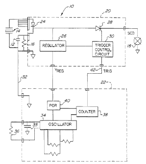
An electronic detonator delay circuit in accordance with a particular embodi-
ment of the present invention is illustrated schematically in Figure 1 with a
piezoelec-
tric transducer 14 and a semiconductor bridge 18. Delay circuit 10 comprises a
vari-
ety of circuit elements that may include discrete circuit elements and/or
inte2rated cir-
cuits. Delay circuit 10 comprises, for example, a storage capacitor 12 that
serves as a
storage means for the assembly to receive and store a charge of electrical
energy from
an initiation signal means. In the illustrated embodiment, the electrical
initiation siQ-
CA 02272712 1999-OS-26
WO 98/26248 PCT/US97/22404
-6-
nal is obtained from a piezoelectric transducer 14 which produces a pulse of
electrical
energy upon the receipt of a detonation shock wave. The detonation shock wave
may
be obtained from a detonating cord disposed in close proximity to transducer
14, as
suggested by the Jonsson Patent, U.S. 5,133,257. Alternatively, the detonation
shock
wave may be obtained from a booster charge associated with the circuit
assembly, as
described more fully below. The energy produced by transducer 14 is conveyed
to
storage capacitor 12 through a steering diode 24. A bleed resistor 16 is
positioned to
discharge storage capacitor 12 in the event that energy stored by capacitor 12
is not
otherwise discharged by delay circuit 10. Ordinarily, a detonator delay
circuit is de-
signed to initiate an output charge by discharging the storage capacitor
within a delay
interval in the range of from 1 millisecond to 10 seconds from the receipt of
the ini-
tiation signal. Bleed resistor 16 is chosen so that it discharges storage
capacitor 12
over a significantly longer time period than the anticipated delay interval.
For exam-
ple, bleed resistor 16 may be chosen to discharge storage capacitor 12 over a
time pe-
riod of fifteen minutes.
SCB 18 is connected to the output terminal of switching circuit 20 and is thus
operatively connected to storage capacitor 12. The operation of switching
circuit 20 is
controlled by a timer circuit 22. As illustrated, both switching circuit 20
and timer
circuit 22 draw power for their operation from storage capacitor 12, although
in alter-
native embodiments of the invention, separate power sources, such as battery
cells,
may optionally be provided to power these circuits.
Integrated switching circuit 20 comprises a voltage regulator 26, an
integrated
silicon-controlled rectifier (SCR) 28 and a trigger control signal circuit 30.
SCR 28
serves as a switching element through which energy stored in storage capacitor
12 can
2~ be delivered to SCB 18. The operation of SCR 28 is controlled by trigger
circuit 30
which is responsive to a firing signal issued by timer circuit 22. Regulator
26 steps
down the voltage stored in capacitor 12 to provide a power source for trigger
circuit
and for timer circuit 22.
Timer circuit 22 draws power from storage capacitor 12 via lead 32. Timer
30 circuit 22 comprises an oscillator 34, the frequency of which is determined
in part by
a timing capacitor 3~ and by the selection of an external timing resistor 36.
Timer
circuit 22 also comprises a counter 38 and a power-on reset ("POR") circuit
40. Upon
CA 02272712 1999-OS-26
WO 98/Z6248 PCT/US97/22404
-7_
receipt of power from storage capacitor 12 and regulator 26, POR circuit 40
initiates
oscillator 34 and sets counter 38 to a predetermined reset state. In response
to pulses
received from oscillator 34, counter 38 decrements from the reset state and,
when the
predetermined interval is counted, counter 38 issues a firing signal via
firing lead 42.
The firing signal activates trigger circuit 30 which activates SCR 28. The
remaining
stored energy in storage capacitor 12 is then discharged through SCR 28 to SCB
18.
In the illustrated embodiment, switching circuit 20 is formed as an integrated
BiCMOS circuit in which the integrated circuit elements are dielectrically
isolated
(DI) from each other. Timer circuit 22, however, is a conventional CMOS
integrated
circuit and is therefore able to perform its timing and initiation signaling
functions
while drawing minimal energy from storage capacitor 12. The relatively high
imped-
ance of the CMOS timer circuit 22 does not detract from the efficiency with
which
energy is conveyed from storage capacitor 12 to SCB 18. For example, using a
0.5 pf
capacitor and a switching circuit having a 5 ohm discharge impedance,
switching cir-
cult 20 can discharge 50 microJoules (uJ) (i.e., 0.05 milliJoule (mJ)) from
storage ca-
pacitor 12 in about 1 to 3 microseconds to initiate SCB 18. Prior art
circuits, in con-
trast, require at least 0.2~ mJ for the initiation of a bridge initiation
element in the
same time frame. See, e.g., U.S. Patent 5,309,841 to Hartman et al issued May
10,
1994, at column 7, lines 10-15 (5 volts applied for 10 microseconds); and U.S.
Patent
4,708,060 issued to Bickes, Jr. et al issued November 24, 1987, at column 6,
lines 7-
13 (1-5 mJ). The ability to initiate SCB 18 with such a small amount of
electrical en-
ergy improves the reliability of the delay circuit since it is then less
likely that
switching circuit 20 and timer circuit 22 will discharge storage capacitor 12
to such a
degree that it is unable, after the predetermined delay, to initiate SCB 18.
In addition,
smaller time constants of circuits of the present invention contribute to more
uniform
performance among similarly configured circuits.
As a further result of the bifurcation of high voltage and low voltage
functions
of the delay circuit into dielectrically isolated BiCMOS and conventional CMOS
inte-
grated circuits, the overall size of the delay circuit is smaller than
corresponding prior
art CMOS-only circuits such as is shown in U.S. 5,173,569 to Pallanck et al.
This re-
duction in size is attained because certain circuit elements which previously
had to be
discrete units can be incorporated into the integrated circuits. For example,
steering
CA 02272712 1999-OS-26
WO 98/26248 PCT/US97122404
_g-
diode 24 and SCR 28 are formed as part of the dielectrically isolated BiCMOS
switching circuit 20, whereas prior art steering diodes and SCRs could not be
incorpo-
rated into a standard CMOS circuit and so were present as discrete circuit
elements.
In addition, because the DI BiCMOS portion of the circuit can accommodate
higher
voltages than a CMOS circuit, the delay circuit can comprise a smaller storage
capaci-
tor than prior art circuits. Specifically, storage capacitor 12 of the present
invention
can be a ceramic-type capacitor, which is smaller, less expensive and easier
to incor-
porate in delay circuit 10 than prior art storage capacitors, which are
generally of the
wound film type. The size reduction resulting from the bifurcation of the
delay circuit
functions into CMOS and DI BiCMOS portions allows the delay circuitry of the
pres-
ent invention to be incorporated into a detonator having a standard size shell
for a
conventional No. 8 or No. 12 detonator, which are generally cylindrical in
shape and
have a 0.296 inch (0.117 cm) diameter. Therefore, the present invention
provides an
electronic detonator that can be used with the variety of conventional
blasting prod-
ucts such as booster charges, connector devices, etc., that are configured for
standard-
sized detonators, and gives the user the advantages of delays having digitally-
controlled precision. There is even room in the detonator for protective
circuit encap-
sulation, such as encapsulation 15 (Figure 2), which protects the detonator
circuit
from external vibration. In contrast, prior art digitally controlled detonator
circuits ar
so large that they require oversized shells and so cannot be used with many
standard
blasting components.
Figure 2 provides a perspective view of transducer-circuit assembly 55 com-
prising an electronics module 54 that comprises the delay circuit 10 of Figure
1 with
an output initiation means 46 attached thereto. The delay circuit 10 includes
various
circuit components including timer circuit 22, a timing resistor 36, a
switching circuit
20, a storage capacitor 12, a bleed resistor 16 and output leads 37 that
provide an out-
put terminal to which storage capacitor 12 is discharged. These various
components
are mounted on lattice-like portions or traces 41 of a lead frame and, except
for output
leads 37, are disposed within encapsulation 15. In the illustrated embodiment,
the
output initiation means 46 comprises, in addition to semiconductor bridge 18
(which
is connected across output Ieads 37), an initiation charge 46a, which
preferably com-
prises a fine particulate explosive material and an initiation shell 46b that
is crimped
CA 02272712 1999-OS-26
WO 98/26248 PCT/US97/22404
-9-
onto neck region 44 of encapsulation 15 and which holds initiation charge 46a
in en-
ergy transfer relation to semiconductor bridge 18. Initiation charge 46a is
preferably
pressed in initiation shell 46b to a density of less than 80 percent of its
maximum
theoretical density (MTD). Preferably, SCB 18 is secured to output leads 37 in
a
manner that allows SCB 18 to protrude into, and to be surrounded by,
initiation
charge 46a. Alternatively, such materials may be rendered in the form of a
slurry or
bead mix that can be applied onto the SCB. Output initiation means 46 may
comprise
part of the output means of a detonator and may be used, e.g., to initiate the
base
charge or "output" charge of the detonator in which transducer-circuit
assembly 55 is
disposed, as described below.
Encapsulation 15 preferably engages sleeve 21 only along longitudinally ex-
tending protuberant ridges or fins (which are not visible in Figure 2) and
thus estab-
lishes a gap 48 between encapsulation 15 and sleeve 21 at the circumferential
regions
about encapsulation 15 between the fins. As an alternative to fins,
encapsulation 15
may be configured to have protuberant bosses to engage the interior surface of
a sur-
rounding sleeve or detonator shell, or it may be polygonal in cross section
and engage
sleeve 21 along longitudinal apices or edges, or it may have any other
configuration
effective to dissipate shock waves that may be transmitted to the circuit from
the ex-
terior of the device. Generally, such configurations minimize or at least
reduce the
surface area contact between encapsulation 15 and sleeve 21. In addition, some
or all
of encapsulation 15 may comprise a shock-absorbing material. Alternatively,
encap-
sulation 15 may comprise a shock-absorbing material that may optionally make
full
contact with sleeve 21.
In the illustrated embodiment, encapsulation 15 optionally defines scallops 50
that make test leads 52 accessible but which preferably allow the leads to
remain
within the surface profile of encapsulation 15, i.e., the leads preferably do
not extend
into gap 48. If scallops 50 are omitted, it is preferred that the test leads
do not extend
across gap 48 to contact the surrounding enclosure. Accordingly, before the
electron-
ics module {which comprises the various circuit elements, output initiation
means 46
and encapsulation 15) is placed within sleeve 21, leads such as lead 52 can be
ac-
cessed to test the assembled circuitry. Then, electronics module 54 can be
inserted
into sleeve 21 and leads 52 will not contact sleeve 21.
CA 02272712 1999-OS-26
WO 98/26248 PCT/US97/22404
-10-
Electronics module 54 is designed so that output leads 37 and initiation input
leads 56, through which storage capacitor 12 can be charged, protrude from
respective
opposite ends of electronics module 54. A transducer module 58 comprises a
piezoe-
lectric transducer 14 and two transfer leads 62 enclosed within transducer
encapsula-
tion 64. Transducer encapsulation 64 is dimensioned and configured to engage
~~eve
21 so that transducer module 58 can be secured onto the end of sleeve 21 with
leads
62 in contact with input leads 56. Preferably, encapsulation 15, sleeve 21 and
trans-
ducer encapsulation 64 are dimensioned and configured so that, when assembled
as
shown in Figure 2, an air gap indicated at 66 is established between
encapsulation I5
and transducer encapsulation 64. In this way, electronics module 54 is at
least par-
tially shielded from the detonation shock wave that causes piezoelectric
transducer 14
to create the electrical pulse that initiates electronics module 54. The
pressure im-
posed by such detonation shock wave is transferred through transducer module
58
onto sleeve 21, as indicated by force arrows 68, rather than onto electronics
module
54.
In contrast to prior art detonator delay circuits, in which the various
circuit
packages and elements were mounted on a polymeric or ceramic substrate in a
chip-
on-board type arrangement, the integrated circuits and circuit elements of
delay circuit
10 may be mounted directly on the metal traces 41 of a lead frame. This
assembly
procedure is less costly than prior art procedures and reduces the size of the
delay cir-
cuit, simplifies the integration process and allows for a larger, more
protective encap-
sulation.
Referring now to Figure 3A there is shown one embodiment of a digital delay
detonator 100 comprising an electronics module in accordance with the present
in-
vention. Delay detonator 100 comprises a housing 112 that has an open end 112a
and
a closed end 112b. Housing 112 is made of an electrically conductive material,
usu-
ally aluminum, and is preferably the size and shape of conventional blasting
caps, i.e.,
detonators. Detonator 100 comprises an initiation signal transmission means
for de-
livening an electrical initiation signal to the delay circuit. The initiation
signal trans-
mission means may simply comprise an electrical initiation signal line that
may be
directly connected to the input terminal of a suitably configured delay
circuit in accor-
dance with the present invention. Preferably, however, the detonator is used
as part of
CA 02272712 1999-OS-26
WO 98/26248 PCT/US97122404
-11-
a non-electrical system and the initiation signal transmission means comprises
the end
of a non-electric signal transmission line (e.g., shock tube) and a transducer
for con-
verting the non-electric initiation signal to an electrical signal, as
described herein. In
the illustrated embodiment, the delay detonator 100 is coupled to a non-
electric initia-
tion signal means that comprises, in the illustrated case, a shock tube 110,
booster
charge 120 and transducer module 58. It will be understood that non-electric
signal
transmission lines besides shock tube, such as a detonating cord, low energy
detonat-
ing cord, low velocity shock tube and the like may be used. As is well-known
to
those skilled in the art, shock tube comprises hollow plastic tubing, the
inside wall of
which is coated with an explosive material, so that, upon ignition, a low
energy shock
wave is propagated through the tube. See, for example, Thureson et al, U.S.
Patent
4,607,573, issued August 26, 1986. Shock tube 110 is secured in housing 112 by
an
adapter bushing 114 that surrounds tube 110. Housing 112 is crimped onto
bushing
114 at crimps 116, 116a to secure shock tube 110 in housing 1 I2 and to form
an envi-
ronmentally protective seal between housing 112 and the outer surface of shock
tube
110. A segment 110a of shock tube 110 extends within housing 112 and
terminates at
end 11 Ob in close proximity to, or in abutting contact with, an anti-static
isolation cup
118.
Isolation cup 118 has a friction fit inside housing 112 and is made of a semi-
conductive material, e.g., a carbon-filled polymeric material, so that it
forms a con-
ductive grounding path from shock tube 110 to housing 112 to dissipate any
static
electricity which may travel along shock tube 110. Such isolation cups are
well-
known in the art. See, e.g., U.S. Patent 3,981,240 to Gladden, issued
September 21,
1976. A low energy booster charge I20 is positioned adjacent to anti-static
isolation
cup 118. As best seen in Figure 3B, anti-static isolation cup 118 comprises,
as is
well-known in the art, a generally cylindrical body (which is usually in the
form of a
truncated cone, with the larger diameter end disposed towards the open end
112a of
housing 112) which is divided by a thin, rupturable membrane 118b into an
entry
chamber 118a and an exit chamber 118c. The end I l Ob of shock tube 110
(Figure
3A) is received within entry chamber 118a (shock tube 110 is not shown in
Figure 3B
for clarity of illustration). Exit chamber 118c provides an air space or stand-
off be-
tween the end 11 Ob of shock tube I 10 and booster charge 120 which are
disposed in
CA 02272712 1999-OS-26
WO 98/26248 PCT/US97/22404
-12_
mutual sisal transfer relation to each other. In operation, the shock wave
signal
emitted from end 1 l Ob of shock tube 110 will rupture membrane 118b, traverse
the
stand-off provided by exit chamber 118c and initiate booster charge 120.
Booster charge 120 comprises a small quantity of a primary explosive 124
such as lead azide (or a suitable secondary explosive material such as BNCP),
which
is disposed within a booster shell 132 and upon which is disposed a first
cushion ele-
ment 126 (not shown in Figure 3A for ease of illustration). First cushion
element 126,
which is annular in configuration except for a thin central membrane, is
located be-
tween isolation cup 118 and explosive 124, and serves to protect explosive 124
from
pressure imposed upon it during manufacture.
Isolation cup 118, first cushion element 126, and booster charge 120 may con-
veniently be fitted into a booster shell 132 as shown in Figure 3B. The outer
surface
of isolation cup 118 is in conductive contact with the inner surface of
booster shell
132 which in turn is in conductive contact with housing 112 to provide an
electrical
current path for any static electricity discharged from shock tube 110.
Generally,
booster shell 132 is inserted into housing 112 and housing 112 is crimped to
retain
booster shell 132 therein as well as to protect the contents of housing 112
from the
environment.
A non-conductive buffer 128 (not shown in Figure 3A for ease of illustration),
which is typically 0.015 inch thick, is located between booster charge 120 and
trans-
ducer module 58 to electrically isolate transducer module 58 from booster
charge 120.
Transducer module 58 comprises a piezoelectric transducer (not shown in Figure
3A)
that is disposed in force-communicating relationship with booster charge 120
and so
can convert the output force of booster charge 120 to a pulse of electrical
energy.
Transdt<cer module 58 is operatively connected to electronics module 54 as
shown in
Figure 2. The initiation signal transmission means comprising shock tube
segment
1 l Ob, booster charge 120 and transducer module 58 serves to deliver to delay
circuit
10, in electrical form, a non-electric initiation signal received via shock
tube 110, as
described below.
The enclosure provided by detonator 100 comprises, in addition to housing
112, the optional open-ended steel sleeve 21 that encloses electronics module
54.
Electronics module 54 comprises at its output end an output initiation means
46
CA 02272712 1999-OS-26
WO 98/26248 PCT/US97/22404
-13-
(shown in Figure 2), which comprises part of the output means for the
detonator.
Adjacent to the output initiation means of electronics module 54 is a second
cushion
element 142, which is similar to first cushion element 126. Second cushion
element
142 separates the output end of electronics module 54 from the remainder of
the deto-
nator output means, comprising an output charge 144 that is pressed into the
closed
end 112b of housing 112. Output charge 144 comprises a secondary explosive
144b
that is sensitive to the output initiation means of electronics module 54 and
that has
sufficient shock power to detonate cast booster explosives, dynamite, etc.
Output
charge 144 may optionally comprise a relatively small charge of a primary
explosive
144a for initiating secondary explosive 144b, but primary explosive 144a may
be
omitted if the initiation charge of electronics module 54 has sufficient
output strength
to initiate secondary explosive 144b. The secondary explosive 144b has
sufficient
shock power to rupture housing I 12 and detonate cast booster explosives,
dynamite,
etc., disposed in signal transfer proximity to detonator 100.
I5 In use, a non-electric initiation signal traveling through shock tube 110
is
emitted at end 1 lOb. The signal ruptures membrane 118b of isolation cup 118
and
first cushion element 126 to activate booster charge 120 by initiating primary
explo-
sive 124. Primary explosive 124 generates a detonation shock wave that imposes
an
output force on the piezoelectric generator in transducer module 58. The
piezoelectric
generator is in force-communicating relationship with booster charge 120 and
so con-
verts the output force to an electrical output signal in the fotTn of a pulse
of electrical
energy that is received by electronics module 54. As indicated above,
electronics
module 54 stores the pulse of electric energy and, after a predetermined
delay, re-
leases or conveys the energy to the detonator output means. In the illustrated
em-
bodiment, the charge is released to the output initiation means, which
initiates output
charge 144. Output charge 144 ruptures housing 112 and emits a detonation
output
signal that can be used to initiate other explosive devices, as is well-known
in the art.
While the invention has been described in detail with reference to particular
embodiments thereof, it will be apparent that upon a reading and understanding
of the
foregoing, numerous alterations to the described embodiments will occur to
those
skilled in the art and it is intended to include such alterations within the
scope of the
CA 02272712 1999-OS-26
WO 98/26248 PCT/US97/22404
-14-
appended claims. For example, while the hybrid timer and switching circuit of
the
present invention is illustrated above by an embodiment adapted for use in a
detonator
secured to a non-electric initiation signal transmission line (e.g., shock
tube 110), it
will be understood that the invention can be practiced with detonators secured
to elec-
trical signal transmission lines as well.