Note: Descriptions are shown in the official language in which they were submitted.
CA 02273603 1999-06-04
- 1 -
TITLE: METHOD AND APPARATUS FOR ADAPTIVE CLOCKING FOR
BOUNDARY SCAN TESTING AND DEVICE PROGRAMMING
FIELD OF THE INVENTION
This invention relates to the boundary scan test
techniques and more particularly to a clocking technique
for boundary scan testing and device programming.
BACKGROUND OF THE INVENTION
Boundary Scan Test is a technique which was
originally developed to assist in the testing of printed
circuit boards. The boundary scan technique allows a board
to be tested without requiring the installation of test
pads for conducting the testing.
The Boundary Scan Test protocol was formalized
under IEEE Standard 1149.1 in 1990. Since the adoption of
the IEEE Std. 1149.1, the Boundary Scan Test technique has
proliferated electronics manufacturing and the application
of boundary scan techniques has expanded beyond mere
interconnect testing for printed circuit boards. Today,
boundary scan is being used for microprocessor bus-
emulation, In-System Programming (ISP) of custom
programmable logic devices (CPLD's) and Flash memory
devices, functional testing of ASIC's, and non-scannable
device clusters.
Typically boundary scan testing requires long
test vectors. Since the boundary scan technique is highly
serial and sequential, this results in increased test
execution times. The ability of the controller to shift
data through the scan chain at high frequencies depends on
the delay caused by buffers and drivers and the distance
CA 02273603 1999-06-04
- 2 -
between the target device and scan controller. This means
that the longer the path delay, the slower the TCK clock
rate. In the prior art systems, operation at reasonable
TCK clock rates (5-10MHz) has been achieved by keeping the
distance to within 2-3 inches (5-8 cms) and eliminating any
buffering. In some cases, the use of special pods has been
required. Since boundary scan systems are often used in
manufacturing environments, constraining the distance
and/or using special pods is usually impractical.
In view of these deficiencies with prior art
boundary scan systems, there remains a need for a boundary
scan technique which does not suffer from these
shortcomings.
BRIEF SUMMARY OF THE INVENTION
The present invention provides a boundary scan
method and system which includes adaptive clocking
techniques that compensate for path delays. The adaptive
clocking techniques are suitable for both test applications
and In-System Programming applications.
Advantageously, the adaptive clocking techniques
according to the present invention allow a boundary scan
test bus controller to operate at the maximum TCK clock
rate supported by target devices. Since the effect of path
delay is eliminated by the bus controller, it is no longer
necessary to keep the programming system close to the
target device or mandate the use of special pods.
In addition, the adaptive clocking techniques
according to the present invention eliminate the principle
cause of instability in testing and programming of ISP's.
CA 02273603 1999-06-04
- 3 -
In a first aspect, the present invention provides
a boundary scan controller for scanning a target device,
said boundary scan controller comprising: (a) a clock
generator for generating a system clock; (b) a transmit
module including, (i) a transmit clock generator for
generating a transmit clock, said transmit clock being
derived from said system clock; (ii) an output data
register for storing an output data stream, said output
data register having an output coupled to the target device
and including means responsive to said transmit clock for
shifting said output data stream to the target device; (c)
a receive module having, (i) a receive clock generator for
generating a receive clock, said receive clock being
derived from said system clock and including a delay
counter for delaying the running of said receive clock so
that said receive clock starts running after said transmit
clock; (ii) an input data register for storing data, said
input data register having an input coupled to the target
device and including means responsive to said receive clock
for shifting in an incoming stream of data from the target
device; (d) a state machine controller for controlling the
operation of said transmit module and said receive module
for performing a boundary scan of the target device.
In another aspect, the present invention provides
a method for performing a boundary scan on a target device,
said method comprising the steps of: (a) generating an
output clock for outputting data to the target device; (b)
shifting a serial stream of output data on said output
clock to said target device; (c) generating an input clock
after a predetermined delay for receiving a serial stream
of incoming data from the target device; (d) wherein said
predetermined delay provides a period of time for the
CA 02273603 1999-06-04
- 4 -
target device to respond to said serial stream of output
data.
BRIEF DESCRIPTION OF THE DRAWINGS
Reference will now be made to the accompanying
drawings which show, by way of example, a preferred
embodiment of the present invention, and in which:
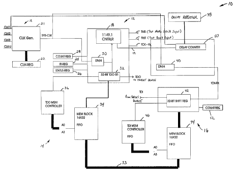
Fig. 1 is a block diagram of a boundary scan
device according to the present invention;
Fig. 2 is a timing diagram showing the
relationship between various clock and control signals for
the boundary scan device of Fig. 1; and
Fig. 3 is a state diagram according to IEEE
Standard 1149.1 for a boundary scan state machine.
DETAILED DESCRIPTION OF THE PREFERRED EMBODIMENT
Reference is first made to Fig. 1 which shows a
boundary scan device according to the present invention and
denoted generally by reference 10. In the context of the
present description, the boundary scan device 10 is
described as a boundary scan controller for a personal
computer based, i.e. "plug&play", test and programming
system.
As shown in Fig. 1, the boundary test controller
10 comprises a clock module 11 and a bus controller 12.
The bus controller 12 comprises a transmit module 14 and a
receive module 16. The transmit module 14 outputs test
data (TDO), i.e. a serial test vector, to a target device
(not shown) on a transmit clock TCK-TX (Fig. 2) as will be
described in more detail below. The receive module 16
CA 02273603 1999-06-04
- 5 -
shifts in test data (TDI) from the target device on a
receive clock TCK-RX (Fig. 2) as will also be described in
more detail below.
The clock module 11 generates a system clock SYS-
CLK which is utilized by the bus controller 12 to generate
the transmit test clock TCK-TX and the receive test clock
TCK-RX. The clock module 11 includes a clock generator
circuit 21 and a clock register 22. The clock generator
circuit 21 comprises circuitry for generating under program
control the system clock SYS-CLK from oscillator clock
inputs CLK1, CLK2, CLK3, and CLK-U. The clock generator 21
is programmable through the clock register 22. The user
determines the frequency for the TCK rate and the SYS-CLK
frequency is automatically calculated from TCK.
In the present embodiment, the oscillator clock
input CLK1 is at 100 MHz, the oscillator clock input CLK2
is at 80 MHz, and the oscillator clock input CLK3 is 66
MHz. Using these oscillator inputs, the clock module 21
generates the user specified frequency for the system clock
SYS-CLK by dividing down the input oscillator frequencies.
For example, if the user specifies a frequency of 50 MHz
for the system clock SYS-CLK, then the clock module 21
divides the oscillator clock input CLK1 by 2 to generate a
50 MHz system clock SYS-CLK. The oscillator clock input
CLK-U is provided for a fourth oscillator circuit for
generating a system clock SYS-CLK which cannot be derived
from the existing oscillator input frequencies.
The bus controller 12 utilizes the clock register
22 to set the desired user frequency for the output test
clock TCK. For example, if a frequency of 25 MHz is
desired for the output clock TCK, the user specifies 25,
CA 02273603 1999-06-04
- 6 -
and the application program interface (API) determines the
desired value for the clock register 22, i.e. CLK-REG, and
writes to the register 22. The circuitry in the clock
module 11 then generates the required frequency for the
system clock SYS-CLK to produce the output clock TCK.
As shown in Fig. 1, the bus controller 12
comprises the transmit module 14 and the receive module 16.
The transmit module 14 controls the transmission of output
test data TDO from the bus controller 12 to the target
device (not shown). The receive module 16, on the other
hand, controls reception of the input test data TDI from
the target device. It is a feature that the transmit
module 14 and the receive module 16 operate independently
from each other and as such facilitate the adaptive
clocking techniques according to the present invention. As
will be described in more detail, this arrangement
eliminates the effects of the pipeline delay on the
transmission speed, and allows the test data TDI to be
shifted-in at the clock rate CLK.
Referring to Fig. 1, the bus controller 12
includes also includes a state machine controller 18. The
function of the state machine controller 18 is to generate
the IEEE Standard 1149.1 compliant signals. As will be
understood by those skilled in the art, the IEEE Std.
1149.1 defines the relationship between various activities
in the boundary scan. The state machine controller 18 is
configured to provide state transitions 200 for "Shift-DR"
mode 201 and "Shift-IR" mode 202 as defined according to
IEEE Std. 1149.1 and reproduced in Fig. 3.
In known manner, the state machine controller 18
has inputs for a Test Mode Select control signal TMS, a
CA 02273603 1999-06-04
- 7 -
Test Reset control signal TRST, and an output for the
transmit test clock TCK-TX for controlling the shifting-out
of the output test data TDO. As shown in Fig. 1, the state
machine controller 18 includes an instruction register 24
or IR-REG, a status register 26 or STATUS-REG, and a
counter register 28 or COUNT-REG.
On power-up, the bus controller 12 puts the state
machine controller 18 into a Test-Logic Reset state. The
state machine 18 stays in this state until an instruction
is received from the instruction register 24. For example,
if it is desired to change the state of the state machine
18 from Reset to Select-DR-Scan (indicated by 201 in Fig.
3), then an appropriate op-code is written to the
instruction register 24. The state machine 18 executes the
op-code in the instruction register 24 and moves to the
Select-DR-Scan state and waits for the next instruction.
The status register 26 or STATUS-REG provides a
report of the activity of the state machine 18 when
performing the shifting of test data. For example, when
the state machine 18 is shifting-out test data, i.e. in
Shift-DR mode (Fig. 3), the output test data TDO is being
shifted-out from an output data memory 34 (as described
below) to the target device (not shown) The status
register 26 reports completion of this activity. It will
be appreciated that subsequent shifts can only happen upon
completion of the current task.
The counter register 28 or COUNT-REG defines the
scan chain length for the target device. The information
from counter register 28 is used by the transmit module 14
and the receive module 16. The value in the counter
register 28 determines the number shifts for the output
CA 02273603 1999-06-04
- 8 -
test data stream TDO and the corresponding input test data
stream TDI.
According to the invention, the transmit module
14 in the bus controller 12 generates its own transmit test
clock TCK-TX for shifting out the output test data TDO to
the target device. As shown in Fig. 1, the transmit module
14 comprises a divide-by-four register 30, an output data
shift register 32, an output data memory module 34, and an
output data memory controller 36. The output memory module
34 provides a block of 32x16 storage for the output test
data TDO and buffers the output shift register 32. The
memory controller 36 controls the transfer of data from the
memory module 34 via four address lines A0, Al, A2 and A3.
The transmit module 14 uses the divide-by-four
register 30 to generate the transmit test clock TCK-TX from
the system clock SYS-CLK, i.e. the transmit clock TCK-TX is
a divided down version of system clock SYS-CLK. For
example, if the system clock SYS-CLK is set at 100 MHz,
then the transmit test clock TCK-TX will be set at 25 MHz
(i.e. 1/4 of the system clock SYS-CLK) . In response to the
shift-out command from the bus controller 12, the output
test data TDO is shifted-out to the target device (not
shown) on the rising edges of pulses in the transmit test
clock TCK-TX (Fig. 2).
As shown in Fig. 1, the output test data TDO is
stored in the memory module 34. In response to control
commands from the state machine 18, the test data TDO is
shifted-out to the target device through the shift register
32 under the control of the output data memory controller
36. When the state machine controller 18 is in Shift-DR
mode (Fig. 3), a double word data i.e. 32-bits, gets loaded
CA 02273603 1999-06-04
- 9 -
from the output data memory module 34 into the output data
shift register 32, then the state machine 18 clocks or
shifts the output test data TDO in the shift register 32 at
the local transmit clock TCK-TX rate. Once the last bit of
the 32-bit output data word is shifted out on an edge (e.g.
rising edge) of the transmit test clock TCK-TX and before
the next rising edge of the transmit test clock TCK-TX, the
transmit memory controller 36 loads the next double word of
output test data TDO (i.e. 32 bits) into the transmit shift
register 32 and the shifting-out process is repeated. It
will be appreciated that this arrangement maintains a
continuous serial stream of output test data TDO and
thereby eliminates any delay or pausing while at the same
time providing a buffer for additional output test data
TDO. The output test data TDO is loaded into the memory 34
from a data bus 33 under the control of the boundary scan
application program.
As described above, the receive module 16 also
generates an independent receive test clock TCK-RX for
shifting in the data TDI from the target device. The
receive module 16 is in charge of collecting the input test
data TDI from the target device.
Referring to Fig. 1, the receive module 16
comprises a divide-by-four register 40, an input data shift
register 42, an input data memory module 44, an input data
memory module controller 46, and a delay register 48. The
input data memory module 44 and the memory module
controller 46 provide a storage block and buffering between
the shift register 42 and the boundary scan application
program.
CA 02273603 1999-06-04
- 10 -
The divide-by-four register 40 generates the
receive test clock TCK-RX by dividing the system clock SYS-
CLK by four. The receive test clock TCK-RX is used to
shift test data TDI from the target device into the shift
register 42. Under the control of the state machine 18,
the input data TDI is shifted into the shift register 42
until 32 bits (i.e. a double word) is received and then
transferred to the input data memory module 44 under the
control of the input data memory controller 46. The input
test data TDI stored in the memory module 44 can then be
transferred over the data bus 33 for further processing by
the boundary scan application program.
The delay register 48 in the receive module 16 is
used to set the amount of delay required to compensate for
pipeline delay before the input test data TDI is shifted
into the shift register 42. The delay factor is given by
the user under program control and is expressed as units of
system clock SYS-CLK periods. For example, a delay factor
of 5 means 5 system clock SYS-CLK periods and at 100MHz.
this translates into a delay of 50 nanoseconds. For
purposes of calculating the delay factor, the system clock
SYS-CLK is always set to 100 MHz irrespective of the
transmit test clock TCK-TX and receive test clock TCK-RX
settings. It will be appreciated that this ensures that
the delay factor is always the same no matter what the
settings are for transmit TCK-TX and receive TCK-RX test
clocks as set by the user. The delay factor stored in the
delay register 48 is used to control a delay counter 50
which counts the delay period for the state machine 18 as
will be described in more detail below.
Reference is now made to Fig. 2, which shows the
adaptive clocking control according to the present
CA 02273603 1999-06-04
- 11 -
invention. Reference is also made to Fig. 3 which shows
the state transitions for the state machine 18 according to
IEEE Std. 1149.1. The adaptive clocking control works for
both Shift-IR and Shift-DR mode of IEEE Standard 1149.1
operation. The state transitions for the Shift-DR mode are
shown in Fig. 3 and denoted generally by reference 201, and
the state transitions for the Shift-IR mode are denoted
generally by reference 202, and will be familiar to the
skilled person in the art.
When the state machine is in the Shift-DR mode
201 or Shift-IR mode 202 of operation, a Start-Shift line
(denoted by reference 19 in Fig. 2) on the bus controller
12 is pulled high at the set-up time for the first bit of
test data TDO to be shifted-out to the target device, i.e.
the state prior to the rising edge 102 of pulses 101 in the
transmit output clock TCK-TX (as shown in Fig. 2) . Pulling
the Start-Shift line 19 HIGH enables the delay-counter 50.
As shown in Fig. 1, the delay counter 50 is clocked
directly by clock CLK1. When the value in the delay-
counter 50 reaches the set value in the delay register 48,
the receive or input data clock TCK-RX is enabled and
pulses 111 are generated based on the set TCK value. As
described above, the delay register 48 sets the delay value
under user control. The pulses 111 (specifically rising
edges 112) of the receive test clock TCK-RX start the
shifting of input test data TDI into the shift register 42.
Once 32 bits of incoming test data TDO have been shifted
into the register 42 on the rising edge 112 of the receive
test clock TCK-RX and before the rising edge 112 of the
next pulse 111 in the receive test clock TCK-RX, the input
data memory controller 46 writes the current value of input
test data (i.e. 32 bits) from the input shift register 42
into the memory module 44. Since this is done between
CA 02273603 1999-06-04
- 12 -
clocking edges of the receive test clock TCK-RX there is no
delay or pause in the reception of the incoming test data
TDI.
It will be appreciated that the delay value is
selected so as to allow the target device sufficient time
to respond to the output test data stream TDO and any other
time delays introduced as a result of the interconnection
between the boundary scan device 10 and the target device.
Provided there is a sufficient delay, the input test data
TDI is shifted in by the receive test clock TCK-RX which
runs at the TCK clock rate.
The present invention may be embodied in other
specific forms without departing from the spirit or
essential characteristics thereof. Certain adaptations and
modifications of the invention will be obvious to those
skilled in the art. Therefore, the presently discussed
embodiments are considered to be illustrative and not
restrictive, the scope of the invention being indicated by
the appended claims rather than the foregoing description,
and all changes which come within the meaning and range of
equivalency of the claims are therefore intended to be
embraced therein.