Note: Descriptions are shown in the official language in which they were submitted.
~
1
r
TITLE
CA 02273665 1999-06-07
Differential Sensing Amplifier for
Content Addressable Memory
s
FIELD OF INVENTION
The present invention generally relates to semiconductor memory devices and
more
specifically to the sensing of matchlines of a high-density Content
Addressable Memory
(CAM) system.
DESCRIPTION OF THE BACKGROUND ART
In general, a semiconductor memory circuit typically consists of an array of
rows and
columns. Each intersection of a row and column defines a memory "cell" that
stores either a
binary logic "1" or a "0".
There are many types of memory available for various storage applications. For
retrieval processing of large amounts of data, an associative memory called
Content
Addressable Memory (CAM) is gaining widespread use in a variety of
applications including
data networking. The important feature of CAM is that it can perform a search
and compare
operation between specified user data and stored data and return match or
mismatch results.
CAM arrays are also made up of intersections of rows and columns of CAM cells,
as
with most typical memories. In addition to rows and columns of cells,
associated with each
row of CAM cells is a matchline and a matchline detection circuit or sense
amplifier that
senses the changes in the logic state of a matchline for the cells in that
row. The matchline
sense amplifier detects a match or a mishmatch during a CAM search and compare
operation.
FIG. 4 illustrates a block diagram of a typical array of memory cells where
the detection
circuit DC is used to sense a match or mismatch on the matchline ML connected
to a row of
several CAM cells.
Conventionally, during matchline sensing, there is no reference level
available to
compare a matchline to be sensed, the selected matchline ML either remains at
a precharged
voltage (VDD, for example) for a match detection, or discharges (towards
ground voltage
VSS, for example) for a mismatch detection. A match or mismatch condition must
be
1
CA 02273665 1999-06-07
.r
detected for each cell in a bit search operation, and every matchline ML must
be sensed
simultaneously with typically 32,000 other matchlines or more. Since
matchlines typically
discharge from the precharged voltage in the case of a mismatch in any bit,
and statistically,
mismatches are much more frequent than matches, dynamic power due to
matchlines
switching simultaneously becomes a significant factor in designing the CAM
which has to be
accounted for.
Moreover, in high-density memory systems where the number of CAM cells in each
row can reach 128 or higher, the speed for discharging a matchline is
virtually limited by the
capacitance of the matchline. This inherent discharge limitation cannot cope
with the fast
switching speed of high-density CAM systems where the search cycle time is of
the order of
l5ns.
A sensing scheme is therefore required that will limit the matchline voltage
swing in
order to reduce the dynamic power of sensing all the matchlines while allowing
for high
speed search operations under low power consumption.
There are several known approaches to designing match/mismatch detection
circuits.
FIG. 1 shows a prior art example for sensing a matchline as disclosed in US
Patent 5,051,948
by Watabe et al. In this sensing scheme, a current-voltage conversion circuit
is first used to
convert the matchline current into a voltage value. This voltage is then
sensed by a voltage
sensing circuit using a dummy reference voltage. This design may not be
suitable for high-
density CAM systems for the following reasons:
a. the current to voltage conversion is performed by a CMOS inverter that is
biased
as an analog amplifier. Under this arrangement, DC power is constantly
consumed
during entire operation and such consumption of power would be well beyond the
limits that a high-density integrated circuit package could handle;
b. The dummy reference voltage circuit also uses CMOS inverters as an analog
amplifier. This scheme not only consumes DC power but also precludes the
appropriate tracking of the reference voltage with that of the matchline under
high-speed, high-density memory sensing conditions; and
c. The circuit blocks of this type of design consume a considerable amount of
integrated circuit area.
In summary, the inhibiting characteristics of this prior art design, when
applied to high-
density CAM systems, are both power and area consumption.
2
,,,
r
CA 02273665 1999-06-07
FIG. 2 shows a second prior art circuit, as disclosed in US Patent 5,012,448,
utilized
in a Read-only-Memory (ROM) multilevel memory. This sensing scheme
incorporates two
CMOS inverters that operate as small-signal amplifiers each connected to NMOS
devices for
current sensing. The sources of both the reference side NMOS and the matchline
side NMOS
are fed into a current minor circuit. As in the first prior art discussed,
this second prior art
approach may not be suitable for high-density memory applications because of
the
unacceptably large dissipation of power. In addition, due to the current
mirror arrangement, a
full CMOS level swing cannot be efficiently achieved.
A third prior art design is disclosed in US Patent 4,763,026 for single-ended
data
sensing. As illustrated in FIG. 3, this approach generates a reference voltage
from the
dataline itself. However, a key disadvantage of this prior art approach is
that the reference
node VREF is allowed to float after being precharged. Based on the high
capacitive load T14,
the precharged voltage value of VREF is expected to remain at the same level
during the
sensing operation. The reliance on a high capacitive load to hold the
precharged value of the
reference node may not be appropriate because, in a VLSI interchip
environment, high noise
injections from high speed operations can corrupt the value of the capacitive
load and cause
an unintended reversal in operation. A second disadvantage of this prior art
design is that
such a large dummy capacitance requires an appreciably large area on the VLSI
chip. This
may be cumbersome and impractical for a high-density CAM arrangement where
32,000 or
more matchline sense amplifiers are required.
In summary, there is clearly a need for matchline sense amplifiers that are
capable of:
~ quickly sensing a (highly capacitive) matchline;
~ limiting the matchline swing; and
~ sense all matchlines simultaneously (32K and above),
but in a manner which reduces the portion of integrated chip area used for
high-density
memory applications and reduces heat dissipation.
SUMMARY OF THE INVENTION
The above identified disadvantages of the prior art are now overcome with a
sensing
amplifier circuit operating under low dynamic power.
It is an object of the present invention to provide a sensing amplifier
circuit for
detecting a change in an input signal at an input node under relatively low
dynamic power
3
CA 02273665 1999-06-07
while consuming relatively little integrated circuit area. In a specifically
preferred
embodiment the invention provides a sensing amplifier circuit for detecting a
match or
mismatch search condition on a high density content addressable memory
matchline that is
capable of:
~ rapidly sensing the capacitive matchline;
~ limiting the matchline voltage swing; and
~ sensing all matchlines simultaneously
~ providing the match and mismatch result for post processing
under relatively low dynamic power while consuming little circuit area.
It is a fiuther objective of the content addressable memory application of the
present
invention to provide a sensing amplifier circuit wherein a sense node to a
differential
amplifier is not allowed to float to an unknown voltage level during the sense
phase in case of
a match and is not affected by noise injection on the matchline from high-
speed operation.
It is yet another objective of the content addressable memory application of
the
present invention to provide a sensing amplifier circuit wherein a reference
node on the
differential amplifier is:
~ allowed to self track the matchline voltage level (including any variation
thereof
due to device mismatches or threshold changes) during the precharge phase and
maintain this precharge level during the sense phase; and
~ not allowed to float after the precharge phase, thus ensuring that noise
coupling
does not corrupt the reference node during the sensing phase.
Therefore, in accordance with one aspect of the present invention, there is
provided a
detection circuit for detecting at an input node a change in an input signal
comprised of four
elements. The first element is a differential amplifier having a sense node
and a reference
node. The second element is a means for alternating the differential amplifier
between a
precharge phase and a sense phase. The third elements is a precharge means for
providing an
input signal precharge voltage to the input signal via an input device, said
input device
selectively coupling the sense node to the input signal upon a change in the
input signal. 'The
fourth element is a reference means for providing the reference node with a
reference signal
that continuously tracks the input precharge voltage during the precharge
phase and actively
maintains the input signal precharge voltage during the sense phase. These
elements
4
~, v
CA 02273665 1999-06-07
comprise an aspect of the invention wherein the detection circuit detects a
change in the input
signal during the sense phase by comparing signals on the sense and reference
nodes.
In an embodiment of the invention a detection circuit as defined above, for
detecting a
match or mismatch search condition on a high density content addressable
memory matchline
wherein the input signal is derived from the matchline.
In accordance with another aspect of the invention, there is provided a method
of
detecting a change in an input signal comprised of five steps. The first step
is to precharge he
input signal to an input signal precharge level. The second step is to
generate a reference
signal that continuously tracks the input signal precharge level during a
precharge phase, and
actively maintaining the reference signal at the input signal precharge level
during a sense
phase. The third step is to derive a sense signal corresponding to the input
signal during the
sense phase. The fourth step is to compare the sense signal with the reference
signal. The
fifth step is to switch an output signal between a first state and a second
state upon said
change.
In accordance with another aspect of the invention, there is provided a
precharge
circuit for precharging a matchline within an array of CAM cells powered from
first and
second power supply terminals, having a predetermined first supply voltage at
the first power
supply terminal relative to the second power supply terminal, comprised of two
elements.
The first element is an input device positioned between the matchline and a
sense node. The
second element is a precharge device for coupling the sense node to the first
power supply
terminal during a precharge phase, wherein an state of the input device is
reversed upon the
matchline reaching a voltage lower than or equal to a pre-selected precharge
voltage, and
wherein the precharge voltage is lower than the first power supply voltage,
all voltages being
in absolute values relative to the second power supply terminal.
In accordance with another aspect of the invention, there is provided a method
of precharging
a matchline during a precharge phase within an array of CAM cells comprised of
two steps.
The first step is to begin to precharge the matchline by coupling the
matchline to a first power
supply terminal via an input device. The second step is to decouple the
matchline from the
first power supply terminal, when the matchline reaches a pre-selected
precharge voltage.
In accordance with another aspect of the invention, there is provided a
detection
circuit for detecting a match or mismatch search condition on a dynamic
content addressable
memory matchline comprised of three elements. The first element is a precharge
means for
5
CA 02273665 1999-06-07
precharging the matchline to a predetermined matchline precharge voltage
during a precharge
phase. The second element is a reference means for generating a reference
voltage which
tracks the matchline precharge voltage during the precharge phase and actively
maintains the
matchline precharge voltage during a sense phase. The third element is a
differential
amplifier for sensing a voltage difference between the reference voltage at a
reference node
and a sense node voltage at a sense node selectively coupled to the matchline
via an input
circuit during the sense phase.
In accordance with another aspect of the invention, there is provided a
detection
circuit for detecting a change on an input signal comprised of three elements.
The first
element is a precharge means for precharging the input signal to a pre-
selected precharge
voltage during a precharge phase. The second element is a reference means for
generating a
reference voltage on a reference node which tracks the precharge voltage
during the
precharge phase and actively maintains the precharge voltage level during a
sense phase. The
third element is a differential amplifier for sensing a voltage difference
between the reference
voltage and a sense node voltage coupled to the input signal.
BRIEF DESCRIPTION OF DRAWINGS
Exemplary embodiments of the invention will now be further described with
references to the drawings wherein:
FIG. 1 illustrates a prior art sensing circuit used in a content addressable
memory,
FIG. 2 illustrates a prior art sensing circuit of the type used in a ROM
multilevel memory,
FIG. 3 illustrates a schematic diagram and timing data of a prior art sense
amplifier used for
detecting a change in a single-ended data line and using a stable reference
voltage derived
from a data line input,
FIG. 4 illustrates in a block diagram, a series of detection circuits
typically used for detecting
a match or mismatch condition on matchlines each connected to several CAM
cells,
FIG.'s Sa and Sb illustrate in a block diagram and a schematic diagram
respectively, a
matchline sense amplifier in accordance with an embodiment of the present
invention,
FIG. 6 illustrates in a schematic diagram, an alternative embodiment of the
present invention.
FIG. 7 is a timing diagram illustrating sequence of signals in the search
operation of FIG. 5
and FIG. 6, and
6
CA 02273665 1999-06-07
DETAILED DESCRIPTION OF THE INVENTION
FIG. 4 illustrates a block diagram of a series of detection circuits typically
used for
detecting a match or mismatch condition on matchlines ML wherein each
matchline is
connected to several CAM cells. The detection circuit DTC is designed to sense
a match or
mismatch between the search data on searchlines SL and SL/ and data stored in
the CAM
cells. As previously mentioned, in modern state-of the-art CAMS, the number n
of CAM
cells in a row connected to a matchline is typically 128, and therefore, with
128 CAM cells
connected to a matchline the capacitance of that matchline is quite
significant, typically
around 100tF or more depending on the process technology used. In addition,
the total
number of matchlines m are typically as high as 30,000, all of which have to
be sensed
simultaneously for modern applications. The large amount of power dissipated
by the
simultaneous sensing of all these highly capacitive matchlines is an important
factor in the
design of a CAM and is addressed by the present invention. The detection
circuit DTC is the
major aspect of the present invention.
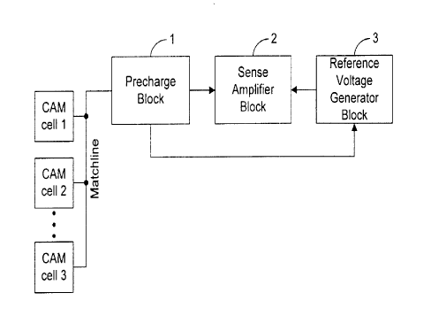
A preferred embodiment of the detection circuit of the invention for use in
CAM
applications for detection of a match or mismatch search condition on a high
density CAM
matchline is illustrated in the block diagram of FIG. Sa. The circuit DTC
consists of a
precharge block 1, a sense amplifier block 2, and a reference voltage
generator block 3. The
precharge block 1 is coupled to the matchline signal and provides the
precharge voltage to the
matchline as well as to the sense amplifier block 2 and the reference voltage
generator block
3. The reference voltage generator block 3 provides the reference voltage to
the sense
amplifier block 2 as will be described in further detail below.
The transistor configuration of FIG. 56 is a detailed implementation of this
preferred
embodiment of the invention. A typical CAM matchline, designated in FIG. 5b as
MATCHLINE, is connected to an input node ML. The input node ML is coupled to a
sense
node SA via a decoupling transistor M2 which is controlled at its gate by a
matchline
decoupling voltage VMLDCPL. The sense node SA is precharged by a precharge
transistor
Ml which is controlled at its gate input by a matchline precharge voltage
pulse MLPREb,
(which is an active-low signal, i.e. it is activated by bringing the signal to
a ground voltage
level). The sense node SA is prevented from floating by a biasing transistor
MS which is
7
CA 02273665 1999-06-07
connected between VDD and node SA. The purpose of the precharge block 1 is to
precharge
the input node ML prior to a search and compare operation.
The sense amplifier block 2, consisting of transistors M10-M18, is preferably
implemented by a differential amplifier (transistors M10, Mll, M18) with a
latching load
(transistors M12-17), a structure which is known to those skilled in the art.
Other sensing
circuits providing the same function as the preferred differential amplifier
can be used as will
be readily apparent to the art skilled person. For sake of simplicity of
description, not due to
their common function, all these circuits will be herein referred to as
differential amplifier
circuits. A sense enable signal MLSEN is provided to the gates of transistors
M18, M16 and
M17 for allowing the differential amplifier to alternate between an active
sensing phase and a
precharge or stand-by phase of operation. The transistors making up the
differential pair,
M10 and Mll, receive at their gates the signals on the sense node SA and on a
reference
node SAref respectively. The differential amplifier circuit 2 performs the
differential sensing
operation as will be described below, and is designed to provide little or no
DC power
dissipation. The power consumed during the latching of a match signal for
example, is
insignificant, and no power is consumed after the latching has occurred.
The reference voltage generator block 3 consists of two serially connected
transistors
between VDD and the reference node SAref. The two transistors M9 and M6
provide a bias
current required to precharge the reference node SAref. Transistor M9 receives
at its gate the
bias voltage VMLBIAS which is also provided to the gate of transistor M5 in
the precharge
block 1. The same matchline decoupling voltage that is provided to the gate of
M2 in the
precharge block 1 is also provided to the gate of transistor M6 in the
reference voltage
generator block 3. Transistor M6 is chosen to have similar operating
parameters as the
decoupling transistor MZ for reasons which will be described in further detail
below.
FIG. Sb shows a number of voltage terminals that are used to supply voltage
levels to
different parts of the sensing circuit. These consist of
~ a first supply terminal VDD - an externally provided or internally generated
power supply
~ a second supply terminal VSS (ground)
~ a pre-selected current-limiting bias voltage VMLBIAS - preferably an on-chip
generated reference voltage
8
CA 02273665 1999-06-07
~ a pre-selected decoupling bias voltage VMLDCPL - preferably an on-chip
generated reference voltage whose value is preferably slightly less than VDD
~ a sense phase enable control signal MLSEN
~ a precharge phase enable control signal MLPREb
It should be noted that in the preferred embodiment, the bias voltage VMLBIAS
and
VMLDCPL are generated on-chip using any conventional voltage-generation
method. More
specifically, the value of VMLDCPL is preferably set slightly lower than VDD
in order to
allow extra noise margin in case of matchline voltage fluctuations. Such
matchline
fluctuations may arise due to charge-sharing between the matchline and
junction nodes of the
CAM cell transistors associated with that matchline. This charge-sharing may
cause the
matchline voltage to drop when search data is loaded into the CAM cells. The
drop on a
matchline connected to an n-bit row of CAM cells will be the final value after
charge-sharing
occurs between the matchline capacitance and the junction capacitance of n
transistors, as a
worst case. If VMLDCPL were set to VDD, this would cause the decoupling
transistor M2 to
turn on for any matchline drop since the gate and the source of the decoupling
transistor M2
will both be at a VDD level and since node SA is precharged to VDD. However,
if
VMLDCPL is set to be below VDD, as in this preferred embodiment, then
matchline
fluctuations will not be sufficiently large to turn on the decoupling
transistor whose gate is
below VDD and whose source is at VDD, and which is therefore maintained in an
off state.
Thus, a lower value of VMLDCPL will provide a greater noise margin.
Furthermore, since
the matchline ML is never precharged to the full VDD level, but rather to
VMLDCPL-Vtn,
where Vtn is the gate-to-source threshold voltage of the decoupling transistor
M2, a
considerable reduction in dynamic power on the matchline is achieved,
representing a key
aspect of this invention.
The reference voltage generating circuit 3 provides a reference signal on the
reference
node SAref. The physical size and current-voltage (I-V) characteristics of the
precharge-
tracking transistor M6 and decoupling transistor M2 are similar in every
respect so that when
the same voltage VMLDCPL is provided to the gates of both M2 and M6, the
voltages on the
reference node SAref and the input node ML (and matchline) are at the same
level. This
unique circuit and component configuration allows the reference voltage on
node SAref to
self track any variations due to device mismatches or threshold voltage
variation. This is
another aspect of the present invention. Transistor M9 provides the bias
current necessary to
9
CA 02273665 1999-06-07
precharge the reference node SAref to the matchline voltage level. The
physical sizes of
transistors M6 and M9 are designed to generate the required reference voltage
level on node
SAref within a relatively short time after the search data is loaded into the
CAM cells.
Furthermore, this active reference generating circuit (M6 and M9) prevents the
reference
node SAref from floating after the precharge phase, ensuring that noise
coupling will not
corrupt the reference node SAref during the sensing phase.
The operation of the embodiment of FIG. Sb will now be described also with
reference to FIG. 6 which is a general simplified timing diagram showing the
precharge and
sense phases of operation. Beginning with a precharge phase prior to a search
and compare
operation, the MLPREb signal supplied to the gate of transistor Ml is pulsed
from VDD to
VSS, causing the sense node SA to become precharged to VDD. The precharge
pulse is
relatively short (about 3.Sns) after which MLPREb returns to VDD, thereby
turning off
transistor Ml. Through the decoupling transistor M2, the input node ML (and
therefore the
matchline) are also precharged to a voltage level equal to VMLDCPL-Vtn. During
this
precharge phase, MLSEN is maintained at VSS level, disabling the differential
sense
amplifier and precharging the single-ended active-low output of the
differential amplifier
outb to VDD level through transistor M16.
Once MLPREb is returned to VDD level, a search and compare operation begins
with
search data being loaded onto the search lines SL and SL/ and being compared
with the
stored data in CAM cells. Assuming a worst-case scenario, where a single bit
mismatch
occurs in the n-bit row of CAM cells, the input node ML (and matchline) start
to discharge
from the VMLDCPL-Vtn level towards VSS, causing the decoupling transistor M2
to turn on
and node SA to drop below reference node SAref by at least 200 mV. Shortly
after this time,
MLSEN is driven to VDD in order to enable the differential sense amplifier and
latch the data
sensed on the gates of the differential pair transistors M10 and Mll. Latching
of a match or
mismatch signal depends on the differential voltage between transistors M10
and Mll when
the control signal MLSEN is enabled to VDD level.
During sensing, if a match is detected between the search data and the data in
the
CAM cells associated with that matchline, the sense node SA remains at VDD
since the
matchline is not discharging, while reference node SAref is at a voltage
threshold level
VMLDCPL-Vtn. This condition causes the differential amplifier to pull down the
output
CA 02273665 1999-06-07
node outb through transistor M10. This output data is latched in the load of
the differential
amplifier and can be used further in the output data path (not shown).
On the other hand, if a mismatch is detected between the search data and at
least one
of the CAM cells associated with the matchline, that matchline voltage
immediately starts to
discharge to VSS, causing M2 to quickly turn on and the voltage on sense node
SA to drop
rapidly to the already discharged matchline level which is well below the
value of
VMLDCPL - Vtn. This rapid drop on node SA, from VDD to below VMLDCPL-Vtn,
occurs
because of the charge-sharing between the small junction and gate capacitance
on sense node
SA and the considerably larger matchline capacitance created by the junction
capacitance of
n CAM cells and wiring capacitance of the matchline. By the time MLSEN is
driven to VDD
(the beginning of the sensing phase) the sense node SA is discharged well
below the
reference node SAref. As a result, this change reverses the gate levels on the
differential pair
M10 and M11 from the match condition, causing the amplifier to pull down node
out and
leave the single ended output outb at VDD level (i.e. at the precharged
level). This output
data is latched in the load of the differential amplifier and can be used
further in the output
data path. The sizes of the latching circuit devices are designed to provide
minimum power
dissipation and load.
The current limiting transistor M5 is biased to operate in the saturation
region by
VMLBIAS in order to provide only a very small constant bias current for
preventing the
sense node SA from floating. It should be noted that the current through the
bias transistor
MS flows only briefly during a mismatch condition and is negligible during a
match
condition. This current through M5 is kept to a minimum so that the pull down
current on the
matchline due to a worst-case single bit mismatch is able to quickly discharge
the matchline
ML. Transistor M5 prevents node SA from floating during the match condition as
well, since
any fluctuation from VDD on node SA will cause MS to clamp node SA back to
VDD. This
current limitation through MS is another key aspect of the invention. In the
prior art, no such
device is included to prevent the differential input node from floating.
FIG. 6 shows a second preferred embodiment of the present invention which is a
design variation of the embodiment of FIG. 5. This second embodiment contains
two
additional transistors M7 and M8 that are used to reset the reference voltage
by allowing
reference node SAref to discharge to VSS during the precharge phase. This is
accomplished
by setting the voltage MLRESET at the gates of M7 and M8 to VDD during the
precharge
11
r
CA 02273665 1999-06-07
phase, a feature which removes any unwanted charges on the node. As shown in
the timing
diagram of FIG. 6, the reset signal MLRESET is pulsed to from VSS to VDD
simultaneously
with MLPREb being pulsed from VDD to VSS during the precharge phase. Since the
search
data is not yet loaded at the time MLRESET returns to VSS, there is no
conflict in timing
between devices M7 and M8 used for the precharge phase and devices M6 and M9
used for
the sensing phase. FIG. 7 also contains one inverter driver on each side of
the latching
circuit. These inverters, consisting of transistors M19 through M22
respectively, are used to
isolate nodes outb and out. This additional feature prevents any design
mismatch in the
latching load devices of the sense amplifier in order to ensure a balanced
operation.
Although this invention has been described within the context of content
addressable
memories, it can be used in many other applications requiring fast, low power
single ended
sensing schemes, such as Read-only-Memories (ROM's) and Flash Memories.
Of course, numerous variations and adaptations may be made to the particular
embodiments of the invention described above, without departing from the
spirit and scope of
the invention, which is defined in the claims.
12