Note: Descriptions are shown in the official language in which they were submitted.
CA 02273732 1999-06-07
P8362/ST3 (2190111998
IMPEDANCE MATCHING CIRCUIT
BACKGROUND OF THE INVENTION
1. Field of the Invention
The present invention relates to an impedance matching circuit, and in
particular, to a line impedance matching circuit.
2. Description of the Related Art
Impedance matching circuits are generally used to efficiently transfer an
energy at a conjunction point where electronic circuits having the different
characteristic impedances are connected to each other, by rendering the
impedances
seen into either side at the conjunction point identical. To this end, it is
necessary
to match line impedances and load impedances of the circuits. When the line
impedances are matched, the maximum power can be provided from the power
supply. Such line impedance matching is necessary not only for a wire terminal
but
",.
also for a wireless terminal,.and the impedances are matched at 50, 75 and
10052
according to the characteristics of the circuits. With the progress of the
electronic
and communication technologies, the consumers of the electronic communication
products demand more qualified services, and in particular, desire to be
provided
with various services with a single product. To accede to the demands, various
electronic circuits having difference characteristics have come to be provided
at the
single communication product. Accordingly, there is a demand for an impedance
matching circuit capable of matching the impedances which are different
according
to the kinds of the services provided by the products.
CA 02273732 2002-02-26
75998-13
SUN~IARY OF THE INVENTION
It is an object of the present invention to
provide an impedance matching circuit for matching different
impedances in a communication system providing various
services.
According to one aspect the invention provides an
impedance matching circuit for a set-top box including a
diplexer disposed at a preceding stage and having an output
impedance, and a network interface having an input impedance
which is different from the output impedance of the
diplexer; wherein said impedance matching circuit is
connected between the diplexer and the network interface for
matching the output impedance of the diplexer to the input
impedance of the network interface; said circuit further
comprising: a transformer having a primary coil and a
secondary coil which is connected to the network interface;
and a resistor connected in parallel with the primary coil
of the transformer.
According to another aspect the invention provides
an impedance matching circuit for a set-top box including a
diplexer disposed at a preceding stage and having an output
impedance and a network .interface having an input impedance
which is different from the output impedance of the
diplexer; wherein said impedance matching circuit is
connected between the diplexer and the network interface for
matching the output impedance of the diplexer to the input
impedance of the network interface; said impedance matching
circuit comprising: a transformer having a primary coil and
a secondary coil which is conneci~ed to the network
interface; a first resistor for connecting a first output of
the diplexer to a first input of the primary coil of the
2
CA 02273732 2002-02-26
75998-13
transformer; and a second resistor for connecting a second
output of the diplexer to a second input of the primary coil
of the transformer.
According to another aspect the invention provides
an impedance matching circuit fo:r a set-top box including a
diplexer disposed at a preceding stage and having an output
impedance, and a network interface having an input impedance
which is different from the output impedance of the
diplexer; wherein said impedance matching circuit is
connected between the diplexer and the network interface for
matching the output impedance of the diplexer to the input
impedance of the network interface; and wherein said
impedance matching circuit comprises: a transformer having a
primary coil and a secondary coil which is connected to the
network interface; a first resistor for connecting a first
output of the diplexer to a first input of the primary coil
of the transformer; a second resistor for connecting a
second output of the diplexer to a second input of the
primary coil of the transformer; and a third resistor
connected in parallel with the primary coil of the
transformer.
The impedance matr_hing circuit recited in the
preceding paragraph may include a first coil connected
between the diplexer and the first resistor; a second coil
connected between the diplexer and the second resistor; a
first capacitor connected between the first resistor and the
primary coil of the transformer, for cutting off a DC
voltage therebetween; and a second capacitor connected
between the second resistor and the primary coil of the
transistor, for cutting off a DC voltage therebetween. A
3
CA 02273732 2002-02-26
75998-13
composite impedance of the first and second coils cancels a
composite impedance of the :First and second capacitors.
In addition, the :impedance matching circuit may
comprise a surge protection element, connected in parallel
to the diplexer, for protecting the impedance matching
circuit from a surge voltage output from the diplexer.
BRIEF DESCRIPTION OF THE DRAWINGS
The above and other objects, features and
advantages of the present invention will become more
apparent from the following detailed description when taken
in conjunction with the accompanying drawings in which like
reference numerals indicate like parts. In the drawings:
FIG. 1 is a block diagram illustrating a set-top
box and a communication network connected thereto according
to an embodiment of the present invention; and
FIG. 2 is a detailed diagram illustrating an
impedance matching circuit (120) of FIG. 1 according to an
embodiment of the present invention.
DETAILED DESCRIPTION OF THE PREFERRED EMBODIMENT
FIG. 1 illustrates a set-top box and a
communication network connected thereto according to an
embodiment of the present invention. In the figure, a host
digital terminal 10 is connected to an end of a data
communication network (e. g., the Internet). Also, the host
digital terminal 10 is connected to an optical network unit
20 through an optica=l line and transmits/receives data using
optical signals. In
3a
CA 02273732 1999-06-07
P83621ST3 (21901/1998
the exemplary embodiment, the digital data is transmitted through the optical
transmission line at the frequence band of 6-40MHz. The optical network unit
20
converts the data transmitted/received through the optical transmission medium
into
electric data, and is connected to a diplexer 30 through a copper twist pair
line.
Also, the diplexer 30 is connected to an analog cable television (CATV) source
40
through a coaxial cable. Here, the analog CATV source 40 may be a base station
or
a TV station which transmits image data of an analog TV. The diplexer 30
multiplexes data received from the optical network unit 20 and the analog CATV
source 40, and applies the multiplexed data to a set-top box 100 through a
coaxial
cable. In general, the analog TV uses a frequence band of 55-750MHz.
Therefore,
the diplexer 30 transmits different the data to the set-top box 100 through
the same
transmission line using the different frequency bands.
In the set-top box 100, a diplexer 110 receives the data output from the
external diplexer 30. The diplexer 110 separates the data received from the
optical
I 5 network unit 20 and the data received from the analog CATV source 40
according
to the frequency bands. The separated data component received from the analog
CATV source 40 is transferred to a CATV tuner 140, and the separated data
.,.
component received from the optical network unit 20 is transferred to a
network
interface 130 via an impedance matching circuit 120 according to the present
invention. The CATV tuner 140, connected to a TV set (not shown), selects
broadcasting channels or tunes the TV set to a particular station. The network
interface 130 is connected to a data processing device such as a computer, and
interfaces the input/output data. Further, the network interface 130 is
impedance-
matched with the dipliexer 110 by the impedance matching circuit 120 according
to the present invention so that the input/output data can be communicated in
the
-4-
CA 02273732 1999-06-07
P8362/ST3 (21901/1998
maximum power.
FIG. 2 illustrates a detailed circuit diagram of the impedance matching
circuit 120 according to the present invention. Although the present invention
will
be described with reference to an embodiment composed of specific elements, it
would be understood by those skilled in the art that other equivalent elements
may
be used in place of the specific elements without departing from the sprint
and
scope of the invention.
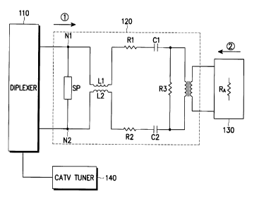
Referring to FIG. 2, a surge protection element SP for protecting the
impedance matching circuit 120 from a surge voltage is connected between first
and
second nodes Nl and N2 where the impedance matching circuit 120 is connected
to the diplexer 110. A first coil Ll, a first resistor Rl and a first
capacitor C1 are
connected in series between the first node N1 and an end of a primary coil of
a
transformer. A second coil L2, a second resistor R2 and a second capacitor C2
are
connected in series between the second node N2 and another end ofthe primary
coil
of the transformer. A secondary,coil of the transformer is connected in
parallel to
the network interface 130. In FIG. 2, the network interface 130 is represented
by an
,,.
input impedance thereof seen at the impedance matching circuit 120. Further,
the
diplexer 110 is connected to the CATV tuner 140.
A 300V surge protection element is used for the surge protection element SP.
Thus, in the case where a telephone set is connected at a following stage of
the
surge protection element SP, the impedance matching circuit 120 can be
prevented
from maloperation due to a ring voltage provided to the telephone set. The
first and
second coils L 1 and L2 prevent the noises incoming from the diplexer 110, and
the
-5-
CA 02273732 1999-06-07
P8362/ST3(21901/1998)
first and second capacitors C 1 and C2 cut off a DC voltage from the diplexer
110.
Also, the coils L 1 and L2 arid the capacitors C 1 and C2 are constructed such
that
their impedances are canceled each other.
The impedance matching circuit 120 has ( 1 ) an input impedance Rs, seen at
the diplexer 110 into the network interface 130 and (2) an output impedance
Rs,
seen at the network interface 130 into the diplexer 110. In the specification,
the
description will be made with reference to specific impedance and resistance,
by
way of example. A resistance RD of the diplexer 110 is set to 10052 for
impedance
matching with the CATV tuner 140. In addition, a resistance of the network
interface 130 is set to 75SZ for impedance matching.
On the assumption that the first and second resistors R1 and R2 are 2552 and
a third resistor R3 connected between both ends of the primary coil of the
transformer is 150SZ, the input impedance will be considered. First, when seen
at the
input side, the third resistor R3 is connected in parallel to a resistance RA
of the
network interface 130 through the transformer. When a composite resistance of
the
parallel-connected resistors is Rs,," the total input impedance Rs, is defined
as a
. ,,.
serial composite resistance of the first and second resistors R1 and R2 and
the
composite resistance Rs.A. Here, the composite resistance RsA can be
calculated by
R,' RA
Rs.a - R~ + RA .... ( 1 )
When calculated in accordance with equation (1), the composite resistance
Rs ~ becomes 5052. Therefore, the total input impedance Rs, seen at the input
side
can be calculated by
-6-
CA 02273732 1999-06-07
P8362/ST3 (21901/1998)
RS ~ - R. + RS..~ + R, .... (2)
When calculated in accordance with equation (2), the total input impedance
RS,, seen at the input side becomes 1005. Accordingly, the impedance matching
is
attained with the diplexer 11Ø
Next, a description will be made as to an output impedance seen at the
network interface 130 into the diplexer 110. When seen at the network
interface
130, the third resistor R3 is first seen. A cascade of the first resistor Rl,
the resistor
R~ of the diplexer 110 and the second resistor R2 is connected in parallel
with the
third resistor R3. A composite resistance RSB of the cascaded resistors R" Rp
and
R, can be calculated by
Rs,~ = R, + Rp + R, .... (3)
When calculated based on equation (3), the composite resistance Rsa
becomes 1 SOS2. In addition, a composite resistance RS, of the resistance RSB
and the
resistance of the third resistor R3 is given by
,,.
RS' Rsa + R~ .... (4)
When calculated based on equation (4), the total output resistance RSZ
becomes 75SZ. Therefore, the impedance matching is attained with the network
interface 130. ..
In this manner, the impedance matching circuit matches an output impedance
CA 02273732 1999-06-07
P8362IST3 (21901/1998
of a circuit at a preceding stage to an input impedance of a circuit at the
following
stage, minimizing the power loss in transmitting/receiving the data.
While the invention has been shown and described with reference to a certain
preferred embodiment thereof, it will be understood by those skilled in the
art that
various changes in fornl and details may be made therein without departing
from
the spirit and scope of the invention as defined by the appended claims.
_g_