Note: Descriptions are shown in the official language in which they were submitted.
' CA 02273752 1999-06-07
W pps\197-0614
ANTI-BRIDGING SOLDER HALL COLLECTION ZONES
BACKGROUND OF THE INVENTION
1. Field of the Invention
The present invention relates generally to printed
circuit boards, and more particularly to a printed circuit
board having improved resistance against solder bridging
and component decentering/tombstoning.
2. Disclosure Information
l5
A conventional printed circuit board (PCB) generally
includes a substrate 10 with conductive circuit traces 30
and mounting pads 14 thereon, as shown in FIGS. 1-3. Once
the traces and pads have been disposed on the substrate, a
thin, solder-resistant layer of material, often called a
"solder mask" 16, is applied to the surface of the PCB.
Typically the solder mask covers substantially all of the
circuit traces, but not the mounting pads; this is
accomplished by forming apertures 18 in the solder mask
25 wherein each aperture generally conforms in shape with and
is situated concentrically about a respective mounting pad.
For example, if a given mounting pad is rectangular, its
corresponding solder mask aperture will likewise be
rectangular, with the edges 22 of the aperture evenly
30 spaced apart from the corresponding edges 28 of the
mounting pad by a given amount or gap P. This gap P
between the mounting pad edges 28 and aperture edges 22 is
referred to as "solder :-cask pullback"; for screenprinting,
the pullback P is typically about 10-20 mils, whereas for
liquid photoimageable solder mask (LPISM) the pullback P is
typically 0-5 mils. As illustrated in ~IGS. 1-3, this
__ 1 __
CA 02273752 1999-06-07
pullback of the mask from the mounting pad creates a
"trough" 32 about each pad.
After the solder mask is applied to the PCB surface,
the mounting pads and any other circuit structures exposed
through the apertures may be tinned, followed by solder
paste being applied thereto, typically by screen-printing
or deposition. Solder paste is typically a slurry of
metallic solder particles (e. g., eutectic tin/lead), flux,
t0 and other components. After the paste has been
printed/deposited, and the PCB has been populated by
placing electronic components thereon with the component
terminations atop their corresponding mounting pads, the
populated PCB is subjected to reflow processing.
During reflow, the metallic component of the solder
paste melts and forms solder joints, while the flux and
other effluent components of the paste are liberated and
often flow across the solder mask surface about each solder
joint. Various gases and vapors are also ejected from the
molten paste during reflow and solidification. It is well
known that when flux and other effluents flow across the
solder mask, they provide solder-wettable paths along which
solder balls may be transported. This presents a serious
?5 problem, because these migratory solder balls may end up
solidifying in such a way as to short out two or more
adjacent mounting pads; or, enough of the solder or paste
may be wicked away from a pad such that the solder that is
left thereon is insufficient to form an acceptable joint
(or any appreciable joint at all), resulting in an open
circuit, or a weak joint if one forms at all.
Additionally, if flux or other effluents wick up underneath
the component 24, the component may "skate" or "float" on
the flux/effluents and become unacceptably decentered with
respect to the mounting pads. Furthermore, gases escaping
from any paste which wicks up under a component may escape
__ 2 __
CA 02273752 1999-06-07
so violently as to promote or worsen the tendency for the
component to decenter or tombstone.
Therefore, it would be advantageous to provide a way
of channeling away and containing the flux and other
effluents liberated during reflow, in order to preclude the
flux/effluents from promoting or exacerbating the
aforementioned problems of solder ball migration and
component decentering and tombstoning.
SUMMARY OF THE INVENTION
The present invention overcomes the disadvantages of
prior art approaches by providing a PCB having improved
resistance against solder bridging and component
decentering/tombstoning. The PCB comprises: (a) a
substrate having a top surface; (b) at least two mounting
pads disposed on the top surface in matched relation with
terminations of an electronic component; and (c) a solder
mask disposed on the top surface and having at least two
apertures therethrough, wherein each aperture generally
conforms in shape with and is arranged about a respective
one of the mounting pads. Each aperture has at least one
inner aperture edge generally within a projected footprint
of the electronic component and at least one outer aperture
edge generally outside the footprint. Each aperture
includes a notch in one or more of the at least one outer
aperture edge, wherein each notch extends generally outward
from its respective mounting pad.
It is an object and advantage of the present invention
that the solder mask aperture notches provide a reservoir
into which solder paste effluents (such as flux) :nay flow
during reflow. This fGcilitates the collection and
~5 containment of effluer_ts and/or solder balls during reflow,
thereby reducing the tendency to form effluent;'f'_ux oaths
__ 3 __
CA 02273752 1999-06-07
across the solder mask surface along which solder balls
could migrate to form solder bridges.
Another advantage is that the present invention acts
to prevent flux/effluents/solder balls from wicking
underneath the component during reflow, thus minimizing or
eliminating the tendency toward component decentering and
tombstoning.
Yet another advantage is that the solder mask notches
of the present invention are easy and inexpensive to
implement, and may be used compatibly and beneficially with
existing solder mask/PCB technology.
These and other advantages, features and objects of
the invention will become apparent from the drawings,
detailed description and claims which follow.
BRIEF DESCRIPTION OF THE DRAWINGS
FIG. 1 is a perspective view of a PCB according to the
prior art.
FIG. 2 is a section view of the PCB of FIG. 1 taken
along line 2-2.
FIG. 3 is a plan view of the PCB of FIG. 1.
FIG. 4 is a perspective view of a PCB according to the
present invention.
FIG. 5 is a section view of the PCB of FIG. 4 taken
along line 5-5.
FIG. 6 is a plan view of the PCB of FIG. 4.
__ 4 __
CA 02273752 1999-06-07
FIGS. 7A-T are plan views of various mounting
pad/solder mask notch configurations according to the
present invention.
FIG. 8 is a plan view of a mounting pad/solder mask
configuration for an 8-pin SOIC (small outline integrated
circuit) according to the present invention.
FIGS. 9A-B are plan views of non-recommended mounting
pad/solder mask notch configurations.
DETAILED DESCRIPTION OF THE PREFERRED EMBODIMENTS
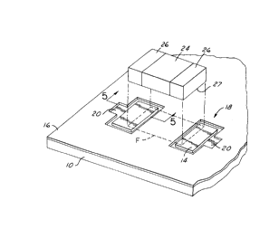
Referring now to the drawings, FIGS. 4-6 show a PCB
having improved resistance against solder bridging and
component decentering/tombstoning according to the present
invention. The PCB comprises: a substrate 10 having a top
surface 12; at least two mounting pads 14 disposed on the
top surface in matched relation with terminations 26 of an
electronic component 24; and a solder mask 16 disposed on
the top surface and having at least two apertures 18
therethrough, wherein each aperture generally conforms in
shape with and is arranged about a respective one of the
mounting pads 14. Each aperture 18 has at least one inner
aperture edge 22i generally within a projected footprint F
of the electronic component and at least one outer aperture
edge 22o generally outside the footprint F. Each aperture
18 includes a notch or relief 20 in one or more of the at
least one outer aperture edge 220, wherein each notch 20
extends generally outward from its respective mounting pad
14.
To assist the reader in understanding the present
invention, all reference numbers used herein are summarized
in the table below, along with the elements they represent:
__ 5 __
CA 02273752 1999-06-07
- Substrate
12 - Top surface of substrate
14 - Mounting pad
16 - Solder mask
18 - Aperture in solder mask
- Notch in solder mask/aperture
20n = Neck portion of notch
22 - Edges of aperture
22i = Inner aperture edge
220 = Outer aperture edge
221 = Lateral outer aperture edge
22a = Axial outer aperture edge
22u = Unnotched portions of outer aperture edge
24 - Electronic component
15 26 - Termination of electronic component
27 - Bottom edge of component
28 - Edges of mounting pad
28i = Inner edge of mounting pad
280 = Outer edge of mounting pad
?0 281 = Lateral outer edge of mounting pad
28a = Axial outer edge of mounting pad
- Circuit traces
32 - Trough
- Molten solder joint
'-5 P - Pullback of solder mask edge from pad edge
P1 - First predetermined distance between 22i
and 28i
Pz - Second predetermined distance between 220
and 2 80 ( excluding note. )
30 P3 - Depth of notch
F - Footprint of electronic component
~1~ - Width of notch
Wo,ai = Width of outer aperture edge having notch
__ o __
CA 02273752 1999-06-07
The substrate 10 may be a conventional flat, planar
FR-4 glass/epoxy laminate; a semi-rigid to rigid plastic
part (e. g., molded out of ABS or polypropylene); a flexible
polyester, polyimide, or polyetherimide film; and so forth.
The mounting pads 14 are typically rectangular or round
copper pads and are formed on the substrate 10 by well-
known plating and etching processes. The electronic
component 24 is preferably a surface mount component (SMC)
with two or more terminations 26 thereon. However, the
mounting pads 14 may instead be plated through-holes or
vias, which extend all the way through the substrate 10,
and the component 24 may be a plated through-hole (PTH)
component with two or more leads 26 extending outward
therefrom.
t5
As in the prior art, the solder mask 16 is a generally
non-solder-wettable layer attached to the top surface 12 of
the substrate 10. The mask 16 has two or more apertures 18
therein, wherein each aperture generally conforms in shape
with, and is arranged about a respective one of, the
mounting pads 14. For example, if a given mounting pad is
rectangular, the corresponding aperture about this pad will
be similarly rectangular (and usually, but not necessarily,
larger in length and width than the pad).
As illustrated in FIGS. 4-6, each aperture 18 has at
least one inner aperture edge 22i generally within a
projected footprint F of the component 24. The footprint F
generally conforms to the underside surface of the
component 24 as projected onto the substrate top surface
12. Each aperture 18 also includes at least one outer
aperture edge 22o generally outside the footprint F. Each
inner aperture edge 22i is generally disposed along and
proximate to a corresponding inner mounting pad edge 28i
pith a first predetermined distance or gap P: therebet:neen,
mhile each outer aperture edge 22o is generally disposed
__
CA 02273752 1999-06-07
along and proximate to a corresponding outer mounting pad
edge 28o with a second predetermined distance or gap PZ
therebetween. Typically, pullback gaps P1 and PZ are the
same as the corresponding prior art pullback measurements
(i.e., 10-20 mils for screenprinted solder mask, and 0-5
mils for LPISM). The depth P3 of each notch 20 from the
adjacent mounting pad outer edge 28o is generally larger
than P1 and Pz, and may be sized depending on the notch
shape chosen, the number and arrangement of notches per
aperture, the effluence/volatility characteristics of the
particular solder paste/processing scheme chosen, and so
forth.
Each aperture 18 further includes a notch or relief 20
in the solder mask/aperture 16/18, in one or more of the at
least one outer aperture edge 220. Each notch 20 extends
generally outward from its respective mounting pad 14, and
may be shaped generally rectangular, round, semi-circular,
T-shaped, or in any other desired shape, as illustrated in
FIGS. 7A-T. More than one notch may be used per aperture,
and more than one notch can be formed in any given outer
edge 220 of the aperture.
It is preferred that each notch 20 have a width wu no
'S greater than about 80~ of the width WoAE of the outer
aperture edge 22o in which the notch is cut. If more than
one notch is located in a given outer edge 220 (as in FIGS.
7G-I), then the combined width EwN of the notches therein
should preferably not exceed about 80~ of the outer edge
width T'~pAE. Alternatively, the notch 20 (or notches) in a
given edge 22o may have an overall width greater than WORE,
so long as each notch is provided with a smaller neck
portion 20n, such that she combined width of all neck
portions on that edge 22o is no greater than about 80% of
--Tn either case, ~he width of the notch/neck
portions) is kept generally less than about 800 oz ~.re
__ g __
CA 02273752 1999-06-07
outer edge width so that sufficient solder mask is left
unnotched, such that the molten solder surface tension
forces between the bottom edge 27 of the component 24 and
the unnotched portions 22u of the outer edge 22o keep the
component from being pulled too far onto the mounting pad
14.
This can be more fully appreciated by referring to
FIGS. 9A and 9B. In each of these figures, the width WN of
the notch 20 is wider than recommended; in fact, in FIG.
9B, the width WN of the notch is equal to the width WoAE of
the outer edge 220. In such configurations, during reflow
the effluents may cause enough of the unmasked substrate
top surface 12 to wet such that the molten solder joint 40
and component 24 are pulled so far toward this unmasked and
wetted surface that the component cannot form a sufficient
solder joint at the opposite end. However, when enough of
the outer aperture edge 22o is left unnotched 22u (i.e.,
each notch/neck portion is kept small enough), as in FIGS.
7A-T, then the surface tension forces are less prone to
cause the aforementioned problem.
During reflow, the notch 20 provides a reservoir in
the aperture about each mounting pad, into which the flux
and other paste effluents -- including solder balls -- may
flow and remain contained. This containment keeps the flux
and other effluents from forming tracks or paths across the
solder mask surface, which might otherwise promote or
assist in the migration of solder balls and the formation
of undesirable solder bridges. The aperture/notch
configuration also assists in keeping flux, paste
effluents, and solder balls away from the underside of the
component 24, by providing each notch 20 in an outer edge
220 of the aperture 18. It is preferred that the notc:~(s)
20 be formed in an outer edge 22o rather than an inner edge
22i. If this were not the case -- that is, if the notcb(s)
__ g __
CA 02273752 1999-06-07
were instead formed in the inner edge 22i of the aperture
within the footprint (i.e., underneath the device) -- there
may be a tendency for the component 24 to skate or float on
the collected flux/effluents/solder balls, possibly
resulting in an unacceptably decentered or tombstoned
component. Also, if solder paste were channeled underneath
the component, the gas ejection which normally occurs
during reflow might be violent enough to cause or promote
tombstoning of the component.
to
Two preferred embodiments are illustrated in the
drawings, the first in FIGS. 4-6, 7A-F, 7L, and 7N-O, and
the second in FIGS. 7R-T. In the first embodiment, the at
least one outer aperture edge 22o may comprise either of
two sub-embodiments: (1) a single outer aperture edge which
is generally arcuate, as shown in FIG. 7L, or (2) two
lateral outer aperture edges 221 each contiguous with an
inner aperture edge 22i, and one axial outer aperture edge
22a contiguous with each of the two lateral edges 221. In
?o the latter sub-embodiment, the single axial outer edge 22a
may be generally straight, as in the case of the generally
rectangular outer aperture of FIGS. 7A-F, or it may be
generally arcuate, as in FIGS. 7N-O. In either sub-
embodiment, each aperture 18 includes only a single notch
20, wherein the notch is located generally along the middle
of (1) the one outer aperture edge 220 (as in FIG. 7L) or
(2) the one axial outer aperture edge 22a (as in FIGS. 7A-F
and 7N-O).
In the second embodiment, the same two sub-embodiments
are preferred (i.e., either (1) a single arcuate outer edge
220, or (2) two lateral edges 221 and a single axial edge
22a). However, rather than a single notch located in the
middle of the outer aperture, two notches are provided,
3~ :~~herein each notch is located on a respective side of the
-- i0 --
CA 02273752 1999-06-07
outer aperture flanking/proximate the component footprint
F. These sub-embodiments are illustrated in FIGS. 7R-T.
In the first embodiment, the notch is positioned along
the outer aperture at the farthest point away from the
mounting pad/aperture inner edges 28i/22i. The purpose for
locating the notch here is to provide the flux/effluent/
solder ball reservoir 20 as far away from the component and
the component underside as possible, so that any excess
effluents/etc. are drawn away from where it could otherwise
do the most damage. In the second embodiment, the notches
are placed on either side of the outer aperture right at
the points where any excess effluents need to be drained
away (i.e., right at the component bottom edge 27, so that
15 the flux/effluents/solder balls may be kept from wicking
underneath the component). Either embodiment serves the
same purpose, but one embodiment might prove more effective
for a given component, depending on the component
dimensions, component weight, the termination dimensions,
?0 the materials involved (i.e., the solder, the termination
metals, the component package material, and any coatings
atop the mounting pads), the termination spacings, the
proximity and layout of adjacent components, and so forth.
--'S For applications involving fine-pitch, multiple-
terminated components, it may be preferred to form the
notch 20 in the axial outer edge 22a of the aperture,
rather than in the lateral outer edges 221, since there
would generally be more available board space in the axial
direction in which the relief's or notches may be formed.
As illustrated by the SOIC arrangement in FIG. 8, between
adjacent pads there is generally not as much available room
in which to form notches as in the axial direction.
.5
-- 11 --
CA 02273752 1999-06-07
Although the present invention is preferably used with
components having at least two terminations 26, the notched
aperture configuration may also be utilized with components
having only a single substrate-mounted termination. For
example, a bare die power transistor has a single
metallized bottom surface which serves as a termination,
and two aluminum bond pads on the top surface of the die
which also serve as terminations. The metallized bottom is
typically soldered to a single substrate mounting pad
(which may also serve as a heat sink for the component),
while the two top bond pads may be wirebonded to an
adjacent leadframe; thus, only a single mounting pad 14 is
needed for such a device. Also, the footprint F of such a
component would lie generally within the perimeter or edges
t5 28 of the mounting pad, and the one or more notches 20 in
the solder mask aperture 18 about the pad may extend
outward in any direction, since any direction chosen will
extend outward from the footprint F (and the pad 14).
Thus, any single pad/aperture/notch arrangement shown in
FIGS. 4 through 7T may be utilized with such a single-
terminated component. The optimum size, shape, and number
of notches 20 may be determined for a given component using
the same factors mentioned previously for the two-or-more-
termination case, and the orientation/direction of each
notch would generally be chosen so as to not interfere with
any adjacent components/pads/apertures.
Various other modifications to the present invention
will, no doubt, occur to those skilled in the art to which
3o the present invention pertains. For example, although
reference is made herein to "solder", "solder paste", and
"reflow" processing, the present invention applies equally
~o forming joints with conductive adhesive rather than
solder paste, and optionally using a curing process (e. g.,
5 ultraviolet/infrared/laser radiation, exposure to hot air
or other gases, etc.) rather than reflow processing. also,
-- 12 --
CA 02273752 1999-06-07
it should be noted that no circuit traces are shown in
FIGS. 4 et seq. (for the sake of clarity), although in
actual practice the PCB would include a multiplicity of
traces. Additionally, it should be apparent that it is
preferred that notches) 20 not be placed atop or astraddle
a circuit trace. Other modifications not specifically
mentioned herein are also possible and within the scope of
the present invention. It is the following claims,
including all equivalents, which define the scope of the
present invention.
-- 13 --