Note: Descriptions are shown in the official language in which they were submitted.
CA 02273999 1999-06-03
WO 99/18672 PCT/US98/19959
-1-
Description
IMPROVED CONVERGENCE IN A DIGITAL SIGNAL
AVERAGER
This application claims the benefit of U.S. Provisional
Application No. 601060932, filed October 3, 1997.
Technical Field
This invention relates to the measurement of rapidly changing,
repetitive electronic waveforms. More specifically, the present
invention relates to a method for improving the speed of convergence
to sub-least-significant-bit precision and accuracy for instruments in
which such waveforms are digitized by high-speed analog-to-digital
converters and wherein repeated measurements are averaged to
improve the signal-to-noise ratio and the dynamic range.
Background Art
It is well known that in many scientific fields, a physical
quantity of interest appears in the form of a time-varying voltage.
Such signals may be observed on an oscilloscope or digitized and
recorded with a computer for analysis and display. If the signal is
repetitive with respect to some time, it may be advantageous to digitize
and average the signal over several records. Each record is initiated by
a trigger that is synchronized to the same time or phase in the repetitive
signal. During each record the voltage waveform is sampled at
periodic time intervals and the samples are digitized and stored in
CA 02273999 1999-06-03
WO 99/18672 PCT/US98/19959
-2-
memory. Because the time spans and sampling intervals are identical
for each record, the data from each record can be added to the sum of
the previous records and the final result divided by the number of
records to form the average. Such averaging can improve the signal-
to-noise ratio. A measurement instrument particularly well suited for
rapidly varying signals is a digital signal averager (DSA).
The digitization of the voltage signal at the input to the DSA is
accomplished by an analog-to-digital converter (ADC). The digital
resolution is determined by the number of bits in the ADC, and the
minimum voltage quantization interval is the width of one least-
significant-bit (LSB).
It is well known by those skilled in the art that the signal-to-
noise ratio of the averaged signal improves in proportion to the square
root of the number of records that are averaged, provided the noise is
1 S not time-correlated with the trigger. If the noise on the signal is less
than 1 LSB of the ADC, then the accuracy of the averaged signal is
limited by the size of 1 LSB.
The following example helps to explain the limitation on
accuracy caused by the digital resolution of the ADC. A DSA
designed for recording fast signals might have an input ADC capable
of sampling at two (2) nanosecond intervals with a resolution of sight
bits (256 discrete levels). For the convenience of calculation, assume
that the eight bits of the ADC cover an input voltage range from 0 to
2.55 volts with the ADC output code 0 centered on zero volts and the
output code 255 centered on 2.55 volts. Accordingly, the ADC output
is some multiple of 0.01 volts. Therefore, if the analog signal
CA 02273999 1999-06-03
WO 99/18672 PCT/US98/19959
-3-
amplitude at some particular time relative to the trigger is always 1.004
volts, the ADC will always record 1.00 volts when it samples that
point in the waveform. Consequently, the waveform reconstructed
from the ADC samples will not have a smooth, continuous shape, but
will increase or decrease in abrupt steps of 0.01 volt. Relevant details
of the waveform which are smaller than the 0.01 volt resolution of the
ADC will be lost. The change in voltage corresponding to the change
of the least-significant-bit of the ADC (0.01 volts in this example) is
often termed the voltage bin width.
Figures 1 and 2 illustrate the loss of detail associated with the
voltage bin width. Figure 1 shows an analog input signal to the ADC.
This signal meanders within the limits of two bins defined by the LSB
boundaries at 1.005, 1.015, and 1.025 volts. The center of the lower
bin is at 1.01 volts, and samples within this bin always generate the
ADC code 101. The upper bin is centered at 1.02 volts, and samples
within this bin always yield the ADC code 102. In this example, the
ADC samples the analog input voltage at 2-nanosecond intervals, as
denoted by the dots in Figures 1 and 2. Figure 2 shows the digital
output of the ADC resulting from the sampling of the analog voltage in
Figure 1. Dividing the ADC code by 100 expresses the digital output
in terms of the input voltage. Clearly, the voltage variation details that
fell within 1 LSB at the ADC input are lost in the digital output of the
ADC.
Those skilled in the art will recognize that a standard solution
to the limitations caused by the finite bin width involves the addition
of noise to the signal, as illustrated in Figure 3. In this example, the
CA 02273999 1999-06-03
WO 99/18672 PCT/US98/19959
-4-
instantaneous input voltage at the sampling time is 1.008 volts. This
falls within the amplitude bin defined by ADC code 101, which has bin
boundaries at 1.005 volts and 1.015 volts. In the absence of added
noise, this signal would be reported by the ADC as code 101, which
represents a 1.010 input voltage. To achieve a more accurate
measurement of the voltage, noise is artificially added to the signal.
There are two critical requirements for the added noise. First, the noise
must be random with respect to the trigger and the signal. Second, the
noise must have a zero mean voltage. In this example, the noise has a
uniform or flat distribution of amplitudes, as defined in Figure 4. In
this case, the width of the noise distribution, W, is set equal to the
width of 1 LSB in the ADC. When the signal plus noise is sampled a
large number of times, 80% of the samples will yield ADC code 101,
and 20% of the samples will generate ADC code 100. Consequently,
the average code will be:
(0.80 x 1 O 1 ) (0.20 x 100) 100.8
(1)
which represents an input voltage of 1.008 volts.
While useful for explaining the theory, the flat noise
distribution in Figure 4 is impractical to implement. Prior art devices
typically use the convenient Gaussian noise distribution depicted in
Figure 5. The root-mean-square (rms) noise voltage for this
distribution has a value denoted by a, and the Full Width at Half
Maximum (FWHM) is given by:
FWHM 2.35 (2)
CA 02273999 1999-06-03
WO 99/18672 PCT/US98/19959
-5-
The typical distribution of Gaussian noise used in prior art
devices is random with respect to the trigger and the signal to be
digitized. Furthermore, it has a zero mean and a uniform power
density versus frequency. Hereinafter, Gaussian noise having these
characteristics will be referred to as "white Gaussian noise".
Because the Gaussian curve does not have a linear distribution,
it is not necessarily obvious that replacing the flat noise distribution
with white Gaussian noise will result in a measurement of the input
voltage that is linearly accurate to a small fraction of 1 LSB. However,
by calculating the maximum systematic error caused by the Gaussian
noise in measuring the input voltage after averaging many samples, the
linear accuracy can be proven. The maximum systematic error, D,
occurs when the original signal (and the mean of the noise distribution)
is half way between the center and the edge of a voltage bin. As
shown in Figure 6, the systematic error becomes a negligible fraction
of 1 LSB, when the rms voltage of the white Gaussian noise is greater
than 0.6 LSB. To provide a margin of safety, a z 1 LSB is typically
chosen for the noise amplitude. Under these conditions, the white
Gaussian noise provides essentially the same quality of interpolation
below 1 LSB in the averaged signal as is afforded by the flat noise
distribution.
However, the example employing white Gaussian noise readily
demonstrates how this traditional solution limits the speed of
convergence to a precise answer. The added noise causes a random
error in each sample of the input signal which can be reduced by
averaging the data. The number of samples which must be averaged to
CA 02273999 1999-06-03
WO 99/18672 PCT/US98/19959
-6-
achieve a desired precision in the measured voltage can be calculated
as the square of the product of FWHM of the Gaussian noise and the
inverse of the fraction of one LSB representing the desired precision.
For example, where the FWHM of the Gaussian noise is two (2) LSB,
to achieve a precision of 1/16 LSB in the measured voltage (2 x 16)Z,
or 1024, samples must be averaged.
The discussion to this point has presumed an ADC with voltage
bin widths which are perfectly uniform over the entire measurement
range. This corresponds to zero differential non-linearity (DNL).
However, a practical ADC has a finite differential non-linearity
specification such as ~'/2 LSB. Taking the exemplary eight-bit ADC
having an input voltage range of 0 to 2.55 volts, the voltage bin width
is not a constant 0.01 volts, but can vary from 0.005 to 0.015 volts over
the ADC range. To aid in understanding the errors caused by
differential non-linearity, apply the earlier example of a uniform noise
distribution to the case in Figure 7. In Figure 7, the voltage bin width
for ADC code 101 is only 0.005 volts, while the width for code 100 is
0.015 volts. When the input signal plus the flat noise is sampled many
times, 30% of the samples yield the 101 code and 70% of the samples
return the 100 code. Thus, the computed average voltage for the input
signal is:
(0.30 x 101) (0.70 x 100) 100.3 (3)
which represents an input voltage of 1.003 volts. This result is in error
of 0.005 volts in reference to the true value of 1.008 volts. The
differential non-linearity has caused a 0.005-volt inaccuracy in the
CA 02273999 1999-06-03
WO 99/18672 PCT/US98/19959
_'7_
measurement. This underlying systematic error is independent of the
number of samples averaged.
One method for con ecting the differential non-linearity error is
to trade some of the useful range of the ADC for a decrease in the
systemic error attributable to the DNL. For example, by broadening
the width of the flat noise distribution until it spans approximately 16
times the average width of 1 LSB, the added noise will average the
measurement over 16 adjacent voltage bins. This reduces the
differential non-linearity error by approximately a factor of 16 while
giving up 16/256 or 6.25% of the useful ADC range. Systematic error
from DNL becomes t %2 LSB x 1/16, or ~ 1/32 LSB, after averaging
many samples. Further improvement can be gained by using an even
wider noise distribution with a corresponding reduction in the useful
range of the ADC.
The uniform noise distribution in the previous paragraph has an
rms voltage given by:
W 16 4,6 LSB
2~/'-3 2~
Consequently, the same functionality could be achieved by replacing
the uniform noise with white Gaussian noise having the same value of v,
i.e., 4.6 LSB. This corresponds to an FWHII~i of 10.8 LSB for the
Gaussian distribution. Such a solution raises a serious problem.
Adding the Gaussian noise causes a random error of 10.8 LSB
(FWHM) in a single sample of the voltage. To reduce this error to
1/16 LSB requires averaging (10.8 x 16)Z = 29,860 samples of the
CA 02273999 1999-06-03
WO 99/18672 PCT/US98/19959
_g_
input signal. Clearly, the rate of convergence to a precision and
accuracy of 1/16 LSB is extremely slow with the prior art method of
adding noise.
Another solution to the DNL error problem was solved by Gatti
et al. for the field of pulse height analysis (C. Cottini, E. Gatti, and V.
Svelto, Nucl. Instr. and Meth. 24 (1963) 241). Gatti employed a circuit
generating offsets which incremented by the average bin width of one
LSB, known as a Gatti slider. Although not originally designed for use
in a digital signal averager, the Gatti slider concept can be modified
and advantageously applied to a digital signal averager as follows. The
result is a more efficient method for reducing differential non-linearity.
A series of measurements are taken where the analog input signal is
slid across a predetermined number of average bin widths by adding an
analog voltage offset to the input signal. The analog voltage offset
corresponds to a whole number multiple of the average voltage bin
width and is incremented with each record. The summed analog signal
is digitized and the results are averaged. Accordingly, the error
introduced as a result of the differential non-linearity of the voltage bin
width is reduced by the factor corresponding to the number of voltage
bins across which the summed analog signal is averaged.
Other devices have been previously disclosed. Typical of the
art are those devices disclosed in the following U.S. Patents:
Pat. No. Inventors) Issue Date
4,490,806 Enke et al. Dec. 25, 1984
4,393,372 W. Hoehn Jul. 12, 1983
4,144,577 G. Ley Mar. 13, 1979
3,622,765 W. Anderson Nov. 23, 1971
CA 02273999 1999-06-03
WO 99/18672 PCT/US98/19959
-9-
The 4,490,806 patent discloses a high speed data acquisition
which includes a noise source for improving the dynamic range in the
summed time spectra. The amplitude of the added noise is at least as
large as one LSB of the ADC.
The 3,622,765 patent discloses a means for adding sub-LSB
(SLSB) analog increments to the analog signal before digitizing in the
ADC. The resulting digital waveforms are summed or averaged over
repeated scans. The analog increments are derived from a repetitive,
continuous, incremental waveform, producing N discrete increments.
The '765 device does not compensate for the differential non-linearity
of the ADC. Furthenmore, the '765 device does not disclose a method
of adding discrete, non-linear increments for reducing the error when
averaging a number of records which is less than N.
The 4,144,577 patent discloses a device employing the method
described in the '765 patent. The interpolation step size is intended to
be less than one LSB of the ADC. As with the '765 device, no
compensation is made for the differential non-linearity of the ADC.
Similarly, the '577 patent does not teach a device which permits the
addition of discrete, non-linear increments for error reduction when
sampling less than the optimum number of samples, N.
The 4,393,372 patent discloses a device for increasing the
number of bits by one in a flash ADC encoding an analog signal. The
method adds +%Z LSB and -'/z LSB of analog voltage to the input signal
on alternate samples of the input signal. The '372 device embodied in
discrete components is not designed for interpolating to less than
LSB. Furthermore, the '372 device does not compensate for the
CA 02273999 1999-06-03
WO 99/18672 PCT/US98/19959
-10-
differential non-linearity of the ADC.
The '806, '372, '577, and '765 prior art devices do not correct
for errors introduced by the differential non-linearity of the ADC. As a
result, the prior art devices do not work accurately for all ADC codes.
Additionally, the '372, '577, and '765 prior art devices disclose only
the addition of linear increments or increments derived from a digital
waveform of alternating polarity. Such a practice causes deterioration
of accuracy when the number of records obtained is not a whole-
number multiple of the number of increments in the complete set of
increments.
Thus, it is an object of the present invention to provide a
method for improving the accuracy of an averaged signal when the
noise inherent in the signal is not large compared to 1 LSB, and to
converge to the desired level of accuracy more rapidly than is possible
with prior art.
Another object of the present invention is to provide a method
for reducing the differential non-linearity of the ADC so that the
interpolation to a fraction of 1 LSB is accurate for all ADC codes.
A still further object of the present invention is to provide a
method for producing results which are more precise and more
accurate in a given measurement time than is possible with the noise-
adding prior art, and wherein a means is provided to obtain a faster
solution for interpolating to a fraction of 1 LSB, and a faster solution
for reducing the error caused by the differential non-linearity of the
ADC in the DSA.
Yet another object of the present invention is to provide a
*rB
CA 02273999 1999-06-03
WO 99/18672 PCT/US98/19959
-11-
method wherein non-linear increments can be utilized to permit greater
accuracy when the number of records obtained does not permit the
complete set of increments to be employed.
Disclosure of the Invention
Other objects and advantages will be accomplished by the
present invention which serves to provide a method for improving the
accuracy of an averaged signal when the noise inherent in the signal is
not large compared to 1 LSB. Furthermore, the present invention
provides a method for converging to the desired level of accuracy more
rapidly than is possible with prior art.
The slider offset circuit described below is designed to
compensate for limitations in the voltage bin width and the differential
non-linearity inherent in a conventional analog-to-digital converter
(ADC) when the measurements are averaged over many samples. By
adding the analog offset generated by the slider offset circuit to the
analog signal provided at the analog input, the error introduced during
the digitization process can be minimized.
The analog input signal is obtained from a conventional analog
sensor used for obtaining measurement from a sample. The analog
sensor measures a voltage waveform that is repetitive with respect to
some trigger event. The measured section of the waveform covers
some arbitrary time interval, termed a scan, and the measurement,
termed a record, is averaged over some arbitrary number of scans.
Because of the linutations of a conventional ADC with respect
to resolution and differential non-linearity, the analog signal obtained
CA 02273999 1999-06-03
WO 99/18672 PCT/US98/19959
-12-
from the analog sensor must be conditioned. Conditioning is achieved
using a sub-least-significant-bit (SLSB) slider and a Gatti slider. The
sliders incorporate at least one digital-to-analog converter (DAC) for
generating an analog offset to be added to the analog input signal.
Specifically, the SLSB slider generates an analog offset which is a
fraction of one least-significant-bit (LSB) of the analog-to-digital
converter for improving the effective resolution of the ADC. The Gatti
slider generates an analog offset nominally equal to the average bin
width of one LSB of the ADC to compensate for variations in the
voltage bin width of the ADC. A clock and control unit (CCLJ)
generates timing signals for sequencing the slider offset circuit and
generates the digital values representing the offsets. The analog signal
from the detector is summed with the analog offsets from the SLSB
slider and the Gatti slider by a summing circuit. An ADC digitizes the
1 S summed analog signal. The offsets added by the sliders are held
constant throughout each scan and are changed at the end of each scan.
A slider offset subtraction device removes the offsets
introduced by the SLSB slider and the Gatti slider firom the digital
signal to restore the integrity of the data. Subtraction of the digital
representation of the analog offset can occur either before or after
summing and averaging, and can be skipped where the d.c. offset of
the signal is of no interest, or where the mean of the added offsets is
approximately zero for the averaged number of records.
A processor sums the result of the data acquisition of the
current record with the previous sum from previous records read from
data memory and stores the new sum in data memory. At the
CA 02273999 1999-06-03
WO 99/186?2 PCT/US98/19959
-13-
conclusion of data acquisition, the sum of the records, termed a
spectrum, is transferred to an analysis and storage device, optionally
being conditioned by a digital signal processor.
The incremental offset generated by the SLSB slider comprises
a set of fractions having a common denominator, D, and numerators
which differ from each other by the integer value one ( 1 ). The number
of fractions in the set is equal to the value of the denominator. The
values of the fractions range from zero (0) to D 1 multiplied by the
voltage corresponding to the average width of 1 LSB of the ADC. For
each record, one member of the set of fractions is added to the analog
input signal recorded from the analog sensor. When all members of the
set have been selected, the offset cycle repeats. Because the offset
voltage changes only at the end of a record, ample time is available to
provide the stable, low-noise offset required. Furthermore, because the
amount of the analog offset voltage to be added at the input is
predetermined, the digital representation of that offset is known and
can be subtracted from the output of the ADC.
Accordingly, the SLSB slider provides an increasingly accurate
output from the ADC as more data is averaged. Further, the result will
be obtained in significantly fewer samples than with prior art devices.
Of course, the time resolution of the SLSB slider method is still the
sampling interval of the ADC used, so fast waveforms are recorded
with the same time resolution.
Because the voltage bin width for each LSB is not uniform over
the full range of the ADC, a Gatti slider must be used to reduce the
effective differential non-linearity of a conventional ADC to less than
CA 02273999 1999-06-03
WO 99/18672 PCT/US98/19959
-14-
~ 1/D LSB in order for the SLSB slider to function properly. The
Gatti slider generates offsets which are a multiple of the average bin
width of one LSB. After cycling through the complement of Gatti
slider offsets, the Gatti cycle is repeated. By "sliding" a given
measurement over several adjacent bins, the DNL becomes the average
of the DNL of those bins.
Accordingly, a method exists by combining the SLSB slider
and the Gatti slider with a digital signal averager to provide an
instrument with an improved speed of convergence to sub-least-
significant-bit accuracy and precision. As will be demonstrated in the
description of a preferred embodiment, the speed of convergence is
improved by using predetermined, non-consecutive fractions for the
increments.
Brief Description of the Drawings
The above mentioned features of the invention will become
more clearly understood from the following detailed description of the
invention read together with the drawings in which:
Figure 1 illustrates a small interval of a single scan of a digital
signal averager (DSA), wherein each data point on the waveform
denotes an analog-to-digital converter (ADC) sample, at 2-nanosecond
intervals, the vertical axis being divided into the voltage bin widths of
the ADC, the signal having details of interest as small as one tenth the
voltage bin width and changing significantly in times on the order of a
few nanoseconds;
Figure 2 illustrates the result of digitizing the signal of Figure
CA 02273999 1999-06-03
WO 99118672 PCT/US98/19959
-15-
1;
Figure 3 illustrates the method of interpolation by adding 1
LSB of flat noise to an ADC with zero differential non-linearity, and
focusing specifically on an ADC sample of the analog signal at one
particular time, the input signal voltage being displayed at the left on
the vertical axis, while the ADC output code is noted at the right side;
Figure 4 illustrates the shape of the uniform (or flat) noise
distribution where P(v) is the probability of observing a voltage, v,
from the noise source at any time, the distribution having a zero mean,
a voltage width, W, and an rms voltage of 2~ ;
Figure 5 illustrates the shape of the Gaussian noise distribution,
P(v) being the probability of observing a voltage, v, from the noise
source at any time, with a zero mean and an rms voltage denoted by a,
the Full Width at Half Maximum (FWHM) being 2.35 a;
Figure 6 illustrates 0, the maximum systematic error in
measuring the input voltage, as a function of o, the rms amplitude of the
white Gaussian noise added to the signal, both variables being plotted
as a ratio to the width of 1 least-significant-bit (LSB) in the ADC, the
error being negligible for a > 0.6 LSB;
Figure 7 illustrates the systematic error caused by differential
non-linearity in the ADC;
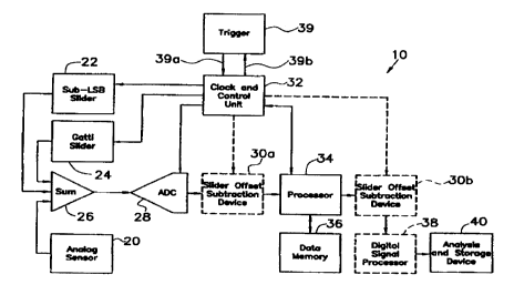
Figure 8 is a block diagram of the slider offset circuit
incorporating various features of the present invention; and
Figure 9 is an expanded view of Figure 1 in the region around
the sample at 32 ns, the sloping solid line representing the input signal
to the DSA, having a voltage of 1.012 volts at the 32 ns sampling
*rB
CA 02273999 1999-06-03
WO 99/18672 PCT/US98/19959
-16-
point, the dashed lines representing the offsets of the input signal
produced by the SLSB slider.
Best Mode for Carryine out the Invention
S The slider offset circuit of the present invention is shown
generally at 10 in the figures. The slider offset circuit 10 is designed to
compensate for limitations in the voltage bin width and the differential
non-linearity inherent in a conventional analog-to-digital converter
(ADC) 28 when the measurements are averaged over many samples.
By adding the analog offset generated by the slider offset circuit 10 to
the analog signal measured by an analog sensor 20, the error
introduced during the digitization process can be minimized.
Figure 8 illustrates a block diagram of the slider offset circuit.
A conventional analog sensor 20 used for obtaining measurement from
a physical or chemical process provides an analog input signal. The
analog sensor 20 produces a voltage waveform that is repetitive with
respect to some trigger event 39, which is synchronized with either the
trigger input 39a or the trigger output 39b. The measured section of
the waveform covers some arbitrary time interval, termed a scan, and
the measurement, termed a record, is averaged over some arbitrary
number of scans. One skilled in the art will recognize that any analog
sensor 20 can be used, however, devices from which the results are
typically averaged are best suited for use with the present invention. In
the illustrated embodiment, the analog sensor 20 is a time-of flight
mass spectrometer.
Because of the limitations of a conventional ADC 28 with
CA 02273999 1999-06-03
WO 99/18672 PCT/US98/19959
-17-
respect to resolution and differential non-linearity, the analog signal
obtained from the analog sensor 20 must be conditioned. Conditioning
is achieved using a sub-least-significant-bit (SLSB) slider 22 and a
Gatti slider 24. Specifically, the SLSB slider 22 generates an analog
offset which is a fraction of one least-significant-bit (LSB) of the
analog-to-digital converter 28 for the purpose of improving the
effective resolution of the ADC 28. The Gatti slider 24 generates an
analog offset with a minimum increment nominally equal to the
average bin width of one LSB of the ADC 28 to compensate for
variations in the voltage bin width of the ADC 28. One skilled in the
art will recognize that the SLSB slider 22 and the Gatti slider 24 can be
implemented in various ways. In the illustrated embodiment, each
slider includes a separate digital-to-analog converter (DAC). Other
implementations can be used such as combining the two sliders into
one common DAC. A clock and control unit (CCL>) 32 generates
timing signals for sequencing the slider offset circuit 10 and generates
the digital values representing the offsets. Each of the SLSB slider 22
and the Gatti slider 24 converts the digital values to an analog offset.
The analog signal from the detector 20 is summed with the analog
offsets from the SLSB slider 22 and the Gatti slider 24 by a summing
circuit such as a summing amplifier 26. An ADC 28 digitizes the
summed analog signal.
A slider offset subtraction device 30 removes the offsets
introduced by the SLSB slider 22 and the Gatti slider 24 from the
digital signal to restore the integrity of the data. Subtraction of the
digital representation of the analog offset added by the SLSB slider 22
CA 02273999 1999-06-03
WO 99/18672 PCT/US98/19959
-18-
and the Gatti slider 24 is accomplished in a variety of ways. In the
preferred embodiment, the digital representation of the net effect of the
slider offsets is subtracted in slider offset subtraction device 30b after
data collection has been completed for the desired number of scans.
Alternatively, the digital representation of the analog offsets is
subtracted from each ADC output value in slider offset subtraction
device 30a. This solution requires broadening the digital bus at the
output of the ADC in order to accommodate the lower order bits
contributed by the SLSB slider 22. Another alternative method
symmetrically steps both sliders either incrementally or decrementally
of alternating polarity about the mean. In this case the residual d.c.
offset caused by the sliders can be negligible when a large number of
scans are averaged. Finally, there are a few applications where the d.c.
offset of the signal is of no interest, where only the AC variations of
the signal are important. In such cases it is not necessary to subtract
the digital representation of the slider offsets, because the offsets show
up as a d.c. offset of the averaged waveform.
A processor 34 sums the result of the data acquisition of the
current record with the previous sum from previous records read from
data memory 36 and stores the new sum in data memory 36. At the
conclusion of data acquisition, the sum of the records, termed a
spectrum, is transferred to an analysis and storage device 40, such as a
conventional computer. The amplitude scale in the spectrum can be
related to the sampled voltage by a variety of methods including
calibration and dividing by the number of scans. One skilled in the art
will recognize that the spectrum can be conditioned using a digital
CA 02273999 1999-06-03
WO 99/18672 PCTlUS98/19959
-19-
signal processor 38; however, one skilled in the art will recognize that
other conditioning or no conditioning could be used.
The signal produced by the slider offset circuit 10 is illustrated
in Figure 9. Figure 9 shows an expansion of the region in the vicinity
of 32 nanoseconds of the sample of Figure 1 including the offsets
generated by the SLSB slider 22. The base analog signal 42 is
illustrated as a solid line having a value of 1.012 volts at 32
nanoseconds. Each broken line represents the base analog signal 42
summed with an incremental offset in voltage generated by the SLSB
slider 22. The incremental offset comprises a small fraction of one
least-significant-bit of the ADC 28. In the illustrated embodiment, the
incremental offset is 1/16 of one LSB of the ADC 28 such that the
offset is zero during the first record 42a, 1/16 of one LSB during the
second record 42b, 2/16 of one LSB during the third record 42c, and so
on up to 15/16 of one LSB during the sixteenth record 42p. On the
seventeenth record, the incremental offset returns to zero and the cycle
repeats.
Because the offset voltage only changes at the end of a record,
ample time is available to provide the stable, low-noise offset required.
Furthermore, because the amount of the analog offset voltage to be
added at the input is predetermined, the digital representation of that
offset is known and can be subtracted from the output of the ADC 28.
Accordingly, the SLSB slider 22 provides an increasingly
accurate output from the ADC 28 as more data is averaged. Further,
the result will be obtained in significantly fewer samples than with
prior art devices. For example, assume sixteen samples are taken at 32
CA 02273999 1999-06-03
WO 99/18672 PCT/US98/19959
-20-
nanoseconds with the special case eight-bit ADC having zero
differential non-linearity (DNL) discussed previously. With each
sample, the offset generated by the SLSB slider 22 increments by 1/16
LSB, or 0.625 mV. For these sixteen records, the ADC 28 returns the
S 101 code five times and the 102 code eleven times. Dividing the ADC
28 codes by 100 to represent the input voltage, the average value
recorded for the voltage is:
5x101 11x102
100 100 1,10169 vol is (5)
16
The result of Equation 5 must be corrected to account for the average
offset added by the SLSB slider 22. This offset is computed as:
0.625mY x (0 1 2 31~. 14 15) 4,69mY (6)
The final result is obtained by subtracting the average offset of
Equation 6 from the average recorded value of Equation S:
1.0169 - 0.00469 1.0122 volts
The result is within 0.2 mV of the correct value. Accordingly,
by increasing the measurement time by a factor of 16, the resolution of
the circuit has been improved by a factor of 16. One skilled in the art
will recognize that a precision s 1/16 LSB is achieved in 16 records
with the SLSB slider 22, whereas the prior art method requires 1024
records to achieve the same precision. Thus, the present invention
CA 02273999 1999-06-03
WO 99/18672 PCT/US98/19959
-21-
enhances speed by a factor of 64 over the prior art. Of course, the time
resolution of the SLSB slider method is still the sampling interval of
the ADC 28 used, so fast waveforms are recorded with the same time
resolution.
The SLSB circuit assumes that the voltage bin width for each
LSB is uniform over the full range of the ADC 28 to better than 1/16
LSB. One skilled in the art will recognize that a typical DNL value for
a conventional ADC 28 is t'/z LSB. Thus, the effective differential
non-linearity of a conventional ADC 28 must be reduced to less than ~
1/16 LSB in order for the SLSB slider 22 to provide interpolation that
has an accuracy of ~ 1/16 LSB. In the illustrated embodiment, a Gatti
slider 24 is employed to correct for the DNL error. The offset on the
first record would be zero. On the second record the offset becomes
one average bin width. The offset increases by one average bin width
up to some maximum, for example 15. One skilled in the art will
recognize that any number of offsets could be used so long as the
number of offsets lowers the effective DNL to a level required by the
SLSB slider 22. The Gatti slider offset is then reset to zero and the
cycle is repeated. By "sliding" a given measurement over several
adjacent bins, the DNL becomes the average of the DNL of those bins.
For example, by using 16 offsets for the Gatti slider 24, the DNL is
reduced from t %2 LSB to approximately t 1/32 LSB.
It will be understood that, though possible, it may not be
practical to make the increment for the Gatti slider 24 exactly equal to
1 LSB of the ADC 28 over the entire range of the ADC 28 because of
the DNL inherent in the ADC 28. However, this fact does not impede
CA 02273999 1999-06-03
WO 99/18672 PCT/US98/19959
-22-
the improvement gained from using the Gatti slider 24, provided the
range of the Gatti slider 24 is large compared to 1 LSB of the ADC 28.
In the present invention, the Gatti slider 24 is combined with
the SLSB slider 22. The digital representation of the analog offset
added by both sliders at the ADC input can be subtracted either at the
ADC output or from the data recorded in memory. The number of
scans required in this invention for the optimum improvement in the
example given becomes 16 (for the Gatti slider 24) times 16 (for the
SLSB slider 22), for a total of 256 scans. This can be compared to the
29,860 scans required for the prior art noise-adding solution.
Accordingly, the present invention converges to a precision and
accuracy less than 1116 LSB approximately 116 times faster than is
possible with the noise-adding prior art.
One skilled in the art will recognize that the increments chosen
for the offsets in the examples above are not intended to limit the
present invention. For example, the sequence of offsets need not be
consecutive. Any sequence which covers each value of the set of
offsets will give the same result. A sixteen number sequence, 0, 7, 14,
3, 10, 6, 13, 2, 9, 5, 12, 1, 8, 15, 4, 11, achieves the same result and
produces smaller errors than a linearly increasing sequence when
executing a number of records which is not a multiple of sixteen.
Furthermore, a pseudo-random sequence of numbers could be used.
When interlacing the increments of the Gatti slider 24 and the
SLSB slider 22, a sequence of numbers can be selected that optimizes
the accuracy when the number of records is less than 256. For
example, consider a slider implementation using an eight-bit DAC that
CA 02273999 1999-06-03
WO 99118672 PCT/US98/19959
-23-
combines the SLSB slider 22 and the Gatti slider 24, with the SLSB
slider 22 occupying the four least-significant-bits and the Gatti slider
24 occupying the four most significant bits. The four least-significant-
bits of the DAC span one LSB of the ADC 28 with sixteen (16) codes
to implement the SLSB slider function. When the clock and control 32
adds 16 to the digital offset, the incremental offset generated by the
DAC adds one LSB in the ADC 28, thus achieving the Gatti slider
function. Incrementing the DAC by seven at the end of each record
generates the following sequence of numbers in the DAC:
0, 7, 14, 21, 28, . . . . . . . , 238, 245, 252;
3, 10, 17, 24, 31, . . . . . , 241, 248, 255;
6, 13, 20, 27, 34, . . . . . . , 237, 244, 251;
2, 9, 16, 23, 30, . . . . . . . , 240, 247, 254;
S, 12, 19, 26, 33, . . . . . . , 236, 243, 250;
1, 8, 15, 22, 29, . . . . . . . , 239, 246, 253;
4, 11, 18, 25, 32, . . . . . . , 235, 242, 249.
In the first row of numbers, the SLSB slider 22 is interpolating
to 7/16 of one ADC bin while the Gatti slider 24 moves through 16
ADC bins. In successive rows the SLSB slider 22 fills in finer
interpolation until it has interpolated to 1/16 of one ADC bin at the end
of the entire sequence of numbers. Compared to incrementing the
DAC by one at the end of each record, incrementing by seven
improves the precision and accuracy of the DSA more quickly when
the number of records is less than 256. Other sequences of numbers
can be used to achieve the same result, including, but not limited to, a
pseudo-random sequence of numbers. Of course, the present invention
CA 02273999 1999-06-03
WO 99/18672 PCT/US98/19959
-24-
may be used with increments other than 16 in each slider.
An object of the present invention is to combine the slider
offset circuit including the SLSB slider and Gatti slider to produce a
high-performance DSA having improved speed in achieving sub-LSB
accuracy and precision with no loss in time resolution. Because the
proposed device relies on averaging the results of many measurements,
it is particularly suited to measurements that require averaging for
other reasons, for example, time-of flight mass spectroscopy.
The present invention provides improved performance when
the inherent noise in the analog signal being measured spans less than
1 LSB in the ADC. The present invention also delivers improved
performance in accurately measuring the baseline between pulses for
cases where the analog signal consists of sparse pulses of low
amplitude superimposed on a baseline voltage that exhibits negligible
noise. The fast interpolation of this baseline voltage to an accuracy
much less than 1 LSB is critical to an accurate measurement of the
amplitudes of the sparse pulses. In such an application this invention
makes the 8-bit ADC used in the example deliver the digital resolution
of a 12-bit ADC after the average of 256 or more records.
If there is a need for even higher resolution, the step size of the
SLSB slider is reduced and the span of the Gatti slider is expanded.
Reducing the step size of the SLSB slider is not necessary, however,
when the inherent noise in the waveform supplied to the input of the
Digital Signal Averager is larger than 1/16 LSB (0.625 mV in the
examples above). Alternatively, white Gaussian noise with an rms
amplitude of the order of 1/16 LSB can be added to the signal via an
CA 02273999 1999-06-03
WO 99/18b72 PCT/US98/19959
-25-
additional input to summing amplifier 26. All of these solutions to
achieve even better accuracy will require a larger number of records.
Having disclosed an apparatus for improving the resolution of a
conventional analog-to-digital converter, it is instructional to describe
a method for using the apparatus. Accordingly, the method for
improving the resolution and rate of convergence of a conventional
ADC includes repetitively sampling a repeatable analog signal to
collect an ensemble of discrete points distributed in time which are
digitized and then averaged to form a digital representation of the
analog signal with improved amplitude resolution.
To improve the resolution of the ADC, two analog offsets are
generated. The first analog offset for implementing the SLSB slider is
formed from a first set of numbers. Each member of the first set of
numbers represents one of a series of integers having a constant
interval and the entire set of numbers spans a range corresponding to a
voltage range approximately equal to an average voltage of one least-
significant-bit of an analog-to-digital converter. The first set of
numbers describes a series having an incremental sequence, a
decremental sequence, or a pseudo-random sequence. Similarly, the
second analog offset implementing a Gatti slider is formed from a
second set of numbers. This second set of numbers defines a series of
integers having a minimum interval corresponding to a voltage range
approximately equal to the average voltage of one least-significant-bit
of the ADC. The interval need not be constant and may vary by an
integer multiple. Likewise, the second set of numbers describes a
series having an incremental sequence, a decremental sequence, or a
CA 02273999 1999-06-03
WO 99/18672 PCT/US98/19959
-26-
pseudo-random sequence.
Once the number sets have been generated, a combination
including one of the first set of numbers and one of the second set of
numbers is selected for use during the current record. No combination
is repeated until every possible combination has been selected. A first
analog voltage offset corresponding to the selected number from the
first set of numbers is generated and a second analog voltage offset
corresponding to the selected number from the second set of numbers
is generated. The analog voltage offsets are summed with the
repeatable analog signal to form a summed signal. Beginning with a
trigger which represents the start of the repeatable analog signal, the
summed signal is digitized a predetermined number of times at a
constant time interval. The collection of these digitizations forms a
record. The digital numbers collected at each acquisition time are
1 S averaged to form averaged data points and stored.
Finally, the digital representations of the analog voltage offsets
are removed from the stored data points to restore the data. One
method for subtracting the first and second analog voltage offsets is to
subtract each number from the currently selected combination from
each discrete digital data point prior to averaging. Alternatively, the
average of the members from each set of numbers selected for the
combination is subtracted from each averaged data point. The
averaged data points may optionally be conditioned by a digital signal
processor prior to storage of the restored data. The method is repeated
until a specified number of said records have been acquired.
From the foregoing description, it will be recognized by those
CA 02273999 1999-06-03
WO 99/18672 PCT/US98/19959
-27-
skilled in the art that a high performance digital signal averager with
distinctly improved performance over prior art and method for use has
been provided. Specifically, the known limitations of high-speed
analog-to-digital converters have been compensated in a unique way,
yielding an instrument with an improved speed of convergence to sub-
least-significant-bit accuracy and precision.
While a preferred embodiment has been shown and described,
it will be understood that it is not intended to limit the disclosure, but
rather the present disclosure and the appended claims are intended to
cover all modifications and alternate methods falling within the spirit
and the scope of the invention as defined in the appended claims.