Note: Descriptions are shown in the official language in which they were submitted.
CA 02274068 1999-06-04
WO 98/25436 PCT/US97/22027
SYSTEM AND METHOD FOR CONTROLLING TIMING IN A
DISTRIBUTED DIGITAL CROSS-CONNECT SYSTEM
TECHNICAL FIELD OF THE INVENTION
This invention relates in general to the field of
telecommunication systems, and more particularly to a
system and method for controlling timing in a distributed
digital cross-connect system.
CA 02274068 1999-06-04
WO 98/25436 PCT/US97/22027
2
BACKGROUND OF THE INVENTION
Telecommunication systems are operable to connect two
or more telecommunications ports through a variety of data
transmission media. For example, a first
telecommunications port may be coupled to a microwave data
transmission medium, which may in turn be coupled to a
copper conductor data transmission medium, then to a fiber
optic data transmission medium, and subsequently to a
second telecommunications port. In this example,
telecommunications data is transmitted through a
telecommunications channel between the first
telecommunications port and the second telecommunications
port via the microwave data transmission medium, the copper
conductor data transmission medium, and the fiber optic
data transmission medium.
Modern telecommunication systems are typically
comprised of a large number of telecommunications ports
connected to a large number of data transmission media.
These media may utilize large signal frequency bandwidths,
such that two or more telecommunications channels may be
combined for transmission over the data transmission media
by multiplexing. In order to connect any given port to any
other given port, it is necessary to utilize specialized
telecommunication switches, which are used to connect the
data transmission media. Such telecommunication switches
CA 02274068 1999-06-04
WO 98125436 - PCT/US97/22027
3
are capable of connecting any of a large number (M) of
input ports to any of a large number (N) of output ports,
with a different data transmission medium connected to each
input and output port. Furthermore, these switches may be
capable of demultiplexing the signal carried over a given
media in order to provide switching capability for
multiplexed telecommunications channels.
A digital cross-connect system is a specialized
telecommunications switch that provides improved
flexibility in switching services. An example of a modern
digital cross-connect system is provided by U.S. Patent No.
5,436,890 to Read et a1 entitled "Integrated Multi-rate
Cross-Connect System," assigned to DSC Communications
Corporation, issued July 25, 1995 (hereinafter "Read"). In
addition. to a telecommunications switch operable to connect
any of r'. input ports to any of N output ports, the digital
cross-c~~ne~~ system taught in Read contains redundant
parallel panes of all components, such that the digital
cros:~ - cr::.-:e_ : system can experience a number of failures in
the cor~::;cnents that comprise both planes without loss of
network t:af=ic.
Lespite the additional flexibility inherent in digital
cross-connect systems, connection of data transmission
media to the digital cross-connect system input ports and
CA 02274068 1999-06-04
WO 98125436 PCT/US97/22027
4
output ports must be coordinated in order to optimize
telecommunications traffic flow. For example, it may be
desirable to transmit telecommunications traffic from an
input port of a first digital cross-connect system to an
output port of a second digital cross-connect system.
While this connection may be accomplished by providing
connections between an output port of the first digital
cross-connect system and an input port of the second
digital cross-connect system, such connections consume
digital cross-connect system resources, i.e., input ports
and output ports.
Furthermore, if two or more separate and discrete
digital cross-connect systems are being used to route
telecommunications traffic, a significant amount of digital
cross-connect system resources must be used to interconnect
the digital cross-connect systems. In many cases, it is
desirable to use two or more physically separated digital
cross connects, such as when a small number of telephony
circuits are connected to network interfaces, but to later
increase the number of digital cross connects and,
subsequently, the number of connections between digital
cross connects, such as when the number of telephony
circuits connected to network interfaces has increased.
Presently available digital cross connect systems do not
readily accommodate such increases in the number of network
CA 02274068 1999-06-04
WO 98/25436 PCT/US97/22027
interfaces, and require network interfaces to be remapped
in order to decrease the number of connections which must
be made between digital cross connect systems.
5
CA 02274068 1999-06-04
WO 98/25436 - PCT/US97J22027
6
SLT_M_NLA_RY OF THE INVENTION
Therefore a need has arisen for a system and method
for connecting a digital cross-connect system to network
interfaces that readily accommodates increases in the
number of network interfaces.
Accordingly, the present invention provides a system
and method for controlling timing in a distributed digital
cross-connect systems that allows data communications to be
transmitted from an input port of a network interface
island to an output port of a network interface island
through a distributed services node.
One aspect of the present invention is a timing system
for coordinating the components of a distributed digital
cross-connect system. The timing system includes a master
timing system, that receives a network timing reference and
generates a master timing signal. A distributed services
node :. _...-r.y system is connected to the master timing system
and receives the master timing signal. The distributed
ser~;;c~~s node timing system then embeds a timing signal in
a da:.a : ra.~.s~:ission frame. Two or more network interface
island :. i.~.:;n~ systems are connected to the distributed
services node timing system and receive the data
transmission frame. The network interface island timing
systems retrieve the embedded timing signal from the data
transmission frame.
CA 02274068 1999-06-04
WO 98/25436 . PCT/LTS97/22027
7
The present invention provides many technical
advantages. One important technical advantage of the
present invention is that two or more network interface
islands may be connected through a distributed services
node in a manner that allows data to be transmitted from an
input port of one network interface island to an output
port of another network interface island.
Another important technical advantage of the present
invention is that the timing systems of physically
separated network interface islands and distributed
services nodes may be coordinated to allow
telecommunications data to be transmitted from a first
network interface island to a second network interface
island through a distributed services node.
CA 02274068 1999-06-04
WO 98/25436 PCT/US97/22027
8
BRIEF DESCRIPTION OF THE DRAWINGS
For a more complete understanding of the present
invention and the advantages thereof, reference is now made
to the following description taken in conjunction with the
accompanying drawings in which like reference numbers
indicate like features and wherein:
FIGURE 1 is a block diagram of an exemplary system
architecture of a distributed digital cross-connect system
embodying concepts of the present invention;
FIGURE 2 is a block diagram of an exemplary unit shelf
control configuration showing the internal configuration of
the network interface island components that control the
connection of the network interface island to the master
interface island and the distributed services nodes;
FIGURE 3 is an exemplary schematic diagram embodying
concepts of the present invention and showing the data
transmission path from digroup circuits of the network
interface island to the unit controller and to the digital
matrix interface;
FIGURE 4 is an exemplary block diagram of the counter-
rotating ring interfaces that are used to receive switching
and control data from the control system communications
media at each network interface island and to transmit
switching and controls data to the control system
CA 02274068 1999-06-04
WO 98/25436 PCT/US97/Z2027
9
communications media from the master network interface
island;
FIGURE 5 is an exemplary schematic diagram showing the
redundant planes of the control structure of the
administration subsystem and the master network interface
island;
FIGURE 6 is an exemplary schematic diagram of a timing
hierarchy embodying concepts of the present invention;
FIGURE 7 is an exemplary schematic diagram of a timing
distribution system embodying concepts of the present
invention;
FIGURES 8A through 8D are exemplary data formats
embodying concepts of the present invention;
FIGURE 9 is a flow chart of an exemplary method for
transmission of data from a first network interface island
to a second network interface island through a distributed
services node;
FIGURE 10 is an exemplary flow chart of a timing
method for a distributed digital cross-connect system; and
FIGURE 11 is an exemplary method for transmitting
digitally-encoded data in accordance with the teachings of
the present invention.
CA 02274068 1999-06-04
WO 98125436 PCT/US97/22027
DETAILED DESCRIPTION OF THE INVENTION
Preferred embodiments of the present invention are
illustrated in the FIGURES, like numerals being used to
refer to like and corresponding parts of the various
5 drawings.
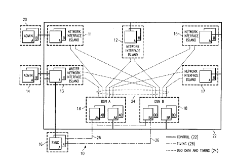
FIGURE 1 is a block diagram of an exemplary system
architecture of a distributed digital cross-connect system
10 embodying concepts of the present invention. As shown
in FIGURE 1, distributed digital cross-connect system 10
10 includes four network interface islands 11, 12, 15, and 17,
a master network interface island 13, an administration
subsystem 14, a synchronization subsystem (SYNC) 16, and
two distributed services nodes (DSN) 18. Distributed
digital cross-connect system 10 also contains provisions
for an optional administration subsystem 20. Network
interface islands 11, 12, 15, and 17, master network
interface island 13, and distributed services nodes 18 are
coupled to control system communications media 22. In
addition, each network interface island 11, 12, 15, and 17
and master network interface island 13 is coupled to each
distributed services node 18 by data and timing media 24.
Synchronization subsystem 16 is coupled to distributed
services nodes 18 by timing signal media 26.
Network interface islands 11, 12, 15, and 17 and
master network interface island 13 comprise M input ports
CA 02274068 1999-06-04
WO 98/25436 _ PCT/US97I22027
11
and N output ports, where "M" and "N" may be any suitable
numbers. For example, a first network interface island 11
may provide distributed digital cross-connect system 10
with 1096 input ports and 1096 output ports, and a second
network interface island 15 may provide digital cross
connect system 10 with 548 input ports and 548 output
ports. These network interface islands are used to provide
telecommunications network interfaces ports through which
telecommunications data transmission channels may be
established.
For example, copper conductor data transmission media
carrying DS1 level signals may be coupled to the input
ports and the output ports of network interface islands 11,
12, 13, 15, and 17. A telecommunications data transmission
channel may need to be established between a first
telecommunications port coupled to a first data
transmission medium that is coupled to an input port of a
first network interface island, such as network interface
island 11, and a second telecommunications port coupled to
a second data transmission medium that is coupled to an
output port of a second network interface island, such as
network interface island 15. The present invention allows
this telecommunications data transmission channel to be
established through the distributed services nodes 18
CA 02274068 1999-06-04
WO 98/25436 PCTIUS97122027
12
without connecting an output port of network interface
island 11 to an input port of network interface island 15.
As shown in FIGURE 1, four network interface islands
11, 12, 15, and 17 and master network interface island 13
are coupled to distributed services nodes 18. Many
suitable numbers of network interface islands may be
connected to distributed services nodes 18. In addition,
as shown in FIGURE 1, each network interface island may
comprise two redundant planes. The use of two redundant
planes is similar to the system and method shown in Read.
Master network interface island 13 may be identical to
network interface islands 11, 12, 15, and 17, and may be
the only network interface island coupled directly to
administration subsystem 14.
Administration subsystem 14 of distributed digital
cross-connect system 10 performs telecommunications routing
and database maintenance for distributed digital cross-
connect system 10. As previously noted, administration
subsystem 14 may be associated with master network
interface island 13, such that communication with network
interface islands 11, 12, 15, and 17 via control system
communications media 22 may require the intermediate step
of transmitting the data to master network interface island
13. Administration subsystem 14 may also be distributed
such that redundant administration subsystems 14 couple to
CA 02274068 1999-06-04
WO 98/25436 _ PCT/US97/22027
13
one or more network interface islands 11, 12, 15, and 17,
or may be in a centralized location and directly coupled to
each network interface island 11, 12, 15, and 17.
The network connections for each network interface
island 11, 12, 15, and 17 are transmitted to administration
subsystem 14 over control system communications media 22.
Likewise, connections established between input ports of
each network interface island 11, 12, 13, 15, and 17 and
output ports of other network interface islands 11, 12, 13,
15, and 17 through distributed services node 18 are
coordinated by administration subsystem 14. Administration
subsystem 14 further performs database maintenance and
telecommunications data transmission channel routing
functions for distributed digital cross-connect system 10.
Synchronization subsystem 16 is a timing subsystem for
coordinating components of distributed digital cross-
connect system 10. Synchronization subsystem 16 may be
associated with master network interface island 13 , in a
manner similar to administration subsystem 14.
Alternately, synchronization subsystem 16 may be centrally
located and couple directly to each subsystem and network
interface island in distributed digital cross-connect
system 10. Synchronization subsystem 16 is a master timing
system that receives network reference timing signals from
the network of data transmission media to which it is
CA 02274068 1999-06-04
WO 98/25436 PCT/US97/22027
14
connected (not explicitly shown). These timing signals are
transmitted to the distributed services nodes timing
systems (not explicitly shown) associated with distributed
services nodes 18. Timing signals are then transmitted to
the timing systems of network interface islands 11, 12, 15,
and 17 and master network interface island 13 via data and
timing media 24.
Distributed services nodes 18 are telecommunications
switches having M input nodes and N output nodes, and form
a telecommunications data transmission path between network
interface islands 11, 12, 15, and 17 and master network
interface island 13. Distributed services nodes 18 may
include data processing equipment for converting optical
signals to electrical signals and for multiplexing and
demultiplexing data, and data processing equipment for
converting between parallel and serial data formats.
Control system communications media 22, data and
timing media 24, and timing signal media 26 are digital
data transmission media, such as copper conductors, coaxial
conductors, optical conductors, or many other suitable
conductors. In the preferred embodiment, control system
communications media 22, data and timing media 24, and
timing signal media 26 are optical conductors to obtain the
highest data transmission speed. Digitally encoded
CA 02274068 1999-06-04
WO 98/25436 PCT/US97/22027
telecommunications data is transmitted over these media in
various data formats.
In operation, data transmission media carrying
dedicated telecommunications channels are coupled to
5 network interface islands 11, 12, 15, and 17 and master
network interface island 13. For example, each network
interface island 11, 12, 15, and 17 and master network
interface island 13 may comprise 1,024 incoming local
telecommunications data channels and 1,024 outgoing local
10 telecommunications data channels. Each network interface
island 11, 12, 15, and 17 and master network interface
island 13 can connect any of the 1,024 incoming local
telecommunications data channels to any of the 1,024
outgoing local telecommunications data channels through
15 distributed services nodes 18. These telecommunications
data channels may be conducted through a single data
transmission medium, such as a fiber optic cable, or
through multiple data transmission media, such as
individual copper conductors.
The connections between network interface islands 11,
12, 15, 17, and master network interface island 13 are
formed through distributed services nodes 18. For example,
data and timing media 24 may each conduct 1,024
telecommunications data channels between network interface
islands 11, 12, 15, 17, and master network interface island
CA 02274068 1999-06-04
WO 98/25436 PCT/US97I22027
16
13 through distributed services nodes 18. These
telecommunications data channels carry telecommunications
data from network interface islands 11, 12, 15, and 17 and
master network interface island 13 to distributed services
nodes 18, and also carry telecommunications data from
distributed services nodes 18 to network interface islands
11, 12, 15, and 17 and master network interface islands 13.
To further illustrate, a telecommunications data
channel may need to be established between an input port of
network interface island 11 and an output port of network
interface island 15. The present invention allows that
telecommunications data channel to be established from
network interface island 11, through distributed services
nodes 18, and to network interface island 15.
In order to transfer digitally-encoded
telecommunications data between network interface islands
11 and 15 and distributed services nodes 18, the timing of
each distributed system must be traceable to a single
common frequency reference. The common frequency reference
for each network interface island 11, 12, 15, and 17,
master network interface island 13, and distributed
services nodes 18 is provided by synchronization subsystem
16. Master network interface island 13 is characterized by
being directly coupled to synchronization subsystem 16.
All other network interface islands are coupled to
CA 02274068 1999-06-04
WO 98/25436 PCT/US97/22027
I7
synchronization subsystem 16 through master network
interface island 13.
The routing of telecommunications traffic is
coordinated by administration subsystem 14. Thus, if
telecommunications traffic must be routed from an input
port of a first network interface island 11 to an output
port of a second network interface island 15, routing
signals received by administration subsystem 14 are first
converted to control signals that may include switching
commands. Next, these control signals are transmitted over
control system communications media 22 from administration
subsystem 14 to network interface islands 11 and 15
involved in the data transmission path, and to distributed
services nodes 18.
In response to these control signals, network
interface islands 11 and 15 and distributed services nodes
18 trat fo::~ the data transmission channel path from the
input pcr~ of the first network interface island 11 to the
outpu: p~:t o~ the second network interface island 15 are
switched :~ ca:ry the telecommunications data channel.
Switching .s synchronized by synchronization subsystem 16
via tirr.:no signals transmitted over timing signal media 26
and data and timing media 24.
One of ordinary skill in the art will recognize that
various changes, substitutions, and alterations can be made
CA 02274068 1999-06-04
WO 98125436 PCT/US97/22027
18
to distributed digital cross-connect system 10 without
departing from the spirit or scope of the present
invention. For example, many suitable numbers of network
interface islands may be used, and that the present
invention is not limited to the four network interface
islands and one master network interface island shown in
FIGURE 1. Likewise, many suitable data communications
media may be used to transmit telecommunications data and
administration and control data between each of the network
interface islands, the master access island, and the
distributed services nodes.
FIGURE 2 is a block diagram of an exemplary unit shelf
control configuration 30 showing the internal configuration
of the network interface island components that control the
connection of the network interface ports of network
interface islands 12, 12, 15, and 17 and of master network
interface island 13 to distributed services nodes 18
(FIGURE 1). These connections are formed from digroup
circuits (DC) 34 to unit controllers (UC) 36, which are
contained within network interface islands 11, 12, 15, and
17 and master network interface island 13, and are
controlled by digital matrix controllers (DMCs) 40 of
access shelves 38. Unit shelf control configuration 30 as
shown includes the access shelves for network interface
islands 11, 12, 15, and 17.
CA 02274068 1999-06-04
WO 98125436 PCT/US97/Z2027
19
Unit shelf control configuration 30 for each network
interface island contains 48 DS1 unit shelves 32 and two
redundant digital matrix controllers 40. DS1 unit shelf 32
may be a discrete telecommunications system component that
includes a number of digroup circuits 34 and unit
controllers 36. For example, DS1 unit shelf 32 may be a
printed circuit board card that includes discrete circuit
components. DS1 unit shelf 32 is comprised of, for
example, 28 individual digroup circuits 34 and two
redundant unit controllers 36. Alternately, DS1 unit shelf
32 may be comprised of more than one discrete
telecommunications system component, such as two printed
circuit boards and a parallel data communications media
connector, and many suitable numbers of digroup circuits 34
and unit controllers 36.
Forty-eight DS1 unit shelves 32 couple to digital
matrix controller 40 of access shelf 38. Each DSl unit
shelf 32 receives a number of serial telecommunications
data streams at a first frequency at digroup circuits 34
from a network interface island. These serial data streams
are converted into a parallel data stream at a second
frequency by unit controller 36. Control data received
from digital matrix controller 40 is embedded into the
parallel data streams.
CA 02274068 1999-06-04
WO 98/25436 PCTIUS97/22027
Digroup circuit 34 may be a discrete
telecommunications switch component, such as an integrated
circuit within a single integrated circuit package, that
receives a single digitally encoded serial data stream or
5 channel from an external telecommunications data
transmission medium. Alternately, digroup circuit 34 may
be comprised of more than one discrete circuit component,
or may be included in a single discrete network interface
island component with one or more other digroup circuits
10 34. For example, digroup circuit 34 may include two or
more integrated circuit packages, discrete components, and
associated conductors.
Unit controller 36 in DS1 unit shelf 32 may be a
discrete telecommunications component, such as a printed
15 circuit card, a separately-packaged integrated circuit, or
similar discrete component. Alternately, unit controller
36 may be comprised of one or more discrete
telecommunications components. Unit controller 36 receives
a plurality of discrete serial telecommunications data
20 channels carrying digitally encoded serial data in a first
data format at a first frequency, converts the first data
format to a second data format at a second frequency, and
includes control data received from digital matrix
controller 40 into the second data format.
CA 02274068 1999-06-04
WO 98125436 PCT/US97/22027
21
For example, digroup circuit 34 may receive a first
serial data format of 8 bit words at a rate of 1.536
megabits per second, and may convert this data to a second
data format of 21-bit words at a rate of 4.032 megabits per
second. Control data received from digital matrix
controller 40 is included in the additional 13 bits of data
in each word by unit controller 36. Unit controller 36 may
also convert the second data format of serial data into a
third data format of parallel data. For example, unit
controller 36 may convert the 21-bit words of serial data
from the 28 digroup circuits 34 into 16-bit words of
parallel data. This parallel data is transmitted to access
shelf 38 at a rate of 5.376 million words per second for
subsequent transmission to distributed services nodes 18.
In addition to digital matrix controller 40, access
shelf 38 may include alarm units, power supplies, and other
suitable components. Digital matrix controller 40 receives
switching and control data from administration system 14
via control system communications media 22 and digroup
circuit 34 inserts this switching and control data into the
data stream being transmitted from digroup circuit 34 to
unit controller 36.
FIGURE 3 is an exemplary schematic diagram 44
embodying concepts of the present invention and showing the
data transmission path from digroup circuits 34 to unit
CA 02274068 1999-06-04
WO 98/25436 PCT/US97/22027
22
controllers 36 and to a digital matrix interface 46. This
data transmission path is also contained within access
shelves 38 (FIGURE 2) of network interface islands 11, 12,
15, and 17 and master network interface island 13 (FIGURE
1). Each digroup circuit 34 receives a DS1 serial
telecommunications data signal comprised of 8-bit words
from an external telecommunications data transmission
media. The 28 digroup circuits 34 are coupled to one unit
controller 36, which converts the 28 8-bit serial
telecommunications data signals into a single 16-bit
parallel data signal for transmission to digital matrix
interface 46. Eight digital matrix interfaces 46 are
contained within one access shelf 38 of FIGURE 3.
Digital matrix interface 46 is a telecommunications
switching component that receives the 16-bit parallel data
signals from unit controllers 36 and multiplexes these
signals into a single signal carrying digitally encoded
data. Digital matrix interface 46 includes a multiplexer
48 which is coupled to a 16-to-10 bit converter 50. 16-to
10 bit converter 50 is coupled to electrical/optical
converter 52. As shown in FIGURE 3, six 16-bit parallel
data signals from unit controllers 36 are received at
multiplexer 48, and are multiplexed into a single 16-bit
parallel data signal that is transmitted to 16-to-10 bit
converter 50. 16-to-10 bit converter 50 converts the 16-
CA 02274068 1999-06-04
WO 98125436 . PCT/US97/22027
23
bit parallel data signal received by multiplexer 48 into a
10-bit parallel data signal. This 10-bit parallel data
signal and other 10-bit parallel data signals from a slave
digital matrix interface 46 is then converted from an
electrical to an optical signal by electrical/optical
converter 52 and is transmitted to distributed services
nodes 18.
After the optical data signal is received at
distributed services nodes 18, it is separated into
individual data channels corresponding to the original DSO
or DS1 data signals in a process that is partially the
reverse of the process shown in FIGURE 3. The optical data
signal is first converted back to two 10-bit parallel
electrical data signals by an optical to electrical
converter (not explicitly shown). The 10-bit parallel data
signals (32,256 10-bit parallel data signals) for the eight
digital matrix interfaces 46 for each access shelf 38 are
then switched through the switching matrix of the
distributed services nodes 18, in addition to the 10-bit
parallel data signals received from other network interface
islands 11, 12, 13, 15, and 17. In the preferred
embodiment, up to 5,376 DSl signals (129,024 DSO signals)
can be switched by the switching matrix of each distributed
services node 18, although any suitable number of matrix
input ports and output ports may be used.
CA 02274068 1999-06-04
WO 98/25436 _ PCT/LTS97I22027
24
At the output port side of the switching matrix in
distributed services nodes 18, two 10-bit parallel data
signals are converted to an optical signal for transmission
to network interface islands 11, 12, 13, 15, and 17. The
optical signal is then converted back into serial DS1 data
streams, which subsequently transmitted over external data
transmission media.
One of ordinary skill in the art will recognize that
various changes, substitutions, and modifications may be
made to the system of FIGURE 3 without departing from the
spirit or scope of the present invention. For example,
many suitable numbers of DS1 signals may be converted from
serial to parallel data, and the size of parallel data
words may be varied from those stated, where suitable for
a given purpose. In addition, the step of converting from
an electrical signal to an optical signal may be omitted,
if ele:;.=:cal signals are transmitted over data and timing
media ~-:. hd~'.:tional error monitoring and alarm equipment,
data pry=~~_~:::.a equipment, and data transmission equipment
may b~ a::~e~ ~o the data transmission path where suitable.
For examp:e, ~ data buffer may be used to temporarily store
data in ~he event of a timing error, to increase the
reliabili~y o' the system.
FIGURE ~ is an exemplary block diagram 54 of the
counter-rotating ring interfaces that are used to receive
CA 02274068 1999-06-04
WO 98/25436 _ PCT/US97/22027
switching and control data from control system
communications media 22 at each network interface island
11, 12, 15, and 17, and to transmit switching and controls
data to control system communications media 22 from master
5 network interface island 13. Block diagram 54 includes
redundant "A" and "B" plane digital matrix controllers 40
for each network interface island 11, I2, 15, and 17 and
master network interface island 13 that are coupled to
clockwise ring "A" 58, counter clockwise ring "A" 60,
10 clockwise ring "B" 62, and counter clockwise ring "B" 64,
which comprise control system communications media 22.
Distributed services nodes 18 are also coupled to clockwise
ring "A" 58, counter clockwise ring "A" 60, clockwise ring
"B" 62, and counter clockwise ring "B" 64.
15 Digital matrix controller 40 receives control and
switching commands from clockwise ring "A" 58, counter
clockwise ring "A" 60, clockwise ring "B" 62, and counter
clockwise ring "B" 64 at the counter-rotating ring
interface shown in block diagram 54. Each network
20 interface island 11, 12, 15, and 17 and master network
interface island 13 contains a digital matrix controller
40, and a corresponding counter-rotating ring interface.
In addition, connections between administration subsystem
14 and clockwise ring "A" 58, counter clockwise ring "A"
25 60, clockwise ring "B" 62, and counter clockwise ring "B"
CA 02274068 1999-06-04
WO 98/25436 PCT/US97/22027
26
64 are made through the digital matrix controller 40 of
master network interface island 13. As previously noted,
each network interface island of network interface islands
11, 12, 15, and 17 and master network interface island 13
contains parallel planes of redundant components. In this
regard, the "A" rings couple to the "A" plane of each
network interface island, and the "B" rings couple to the
"B" plane of each network interface island.
In operation, control and switching commands
determined by administration subsystem 14 are transmitted
on the counter-rotating ring interface of master network
interface island 13 to clockwise ring "A" 58, counter
clockwise ring "A" 60, clockwise ring "B" 62, and counter
clockwise ring "B" 64. Control and switching commands are
then transmitted to each network interface island 11, 12,
15, and 17 through the counter-rotating ring interface of
each network interface island. It should be noted that
control and switching commands for each parallel plane of
the network interface island of network interface islands
11, 12, 15, and I7 are transmitted over two redundant
paths.
For example, for plane A of network interface islands
11, 12, 15, and 17, master network interface island 13, and
distributed services nodes 18, switching and control
commands are transmitted over clockwise ring "A" 58 and
CA 02274068 1999-06-04
WO 98/25436 _ PCT/ITS97/22027
27
counter clockwise ring "A" 60. Likewise, for plane B of
network interface islands 11, 12, 15, and 17, master
network interface island 13, and distributed services nodes
18, switching and control commands are transmitted over
clockwise ring "B" 62 and counter clockwise ring "B" 64.
This configuration ensures that a path between each network
interface island 11, 12, 15, and 17 will be available
following a construction accident or similar break at one
point along clockwise ring "A" 58, counter clockwise ring
"A" 60, clockwise ring "B" 62 or counter clockwise ring "B"
64.
One of ordinary skill in the art will recognize that
various changes, substitutions, and alterations can be made
to the counter-rotating ring interface shown in FIGURE 4
without departing from the spirit or scope of the present
invention. For example, a single set of counter-rotating
rings may be utilized, or the master network interface
island may couple directly to the counter-rotating rings,
if suitable.
FIGURE 5 is an exemplary schematic diagram showing the
redundant planes of control structure 70 of administration
subsystem 14 and master network interface island 13.
Control structure 70 includes digital matrix controllers
(DMC) 40 for the A plane and B plane of the master network
interface island 13, which are coupled to the digital
CA 02274068 1999-06-04
WO 98/25436 PCT/US97/22027
28
matrix interfaces (DMI) 46 of master network interface
island 13. The digital matrix controllers 40 are also
connected to clockwise ring "A" 58, counter clockwise ring
"A" 60, clockwise ring "B" 62 or counter clockwise ring "B"
64, to form the counter-rotating ring interface for master
network interface island 13. Plane "A" of control
structure 70 couples to a single alarm interface (AI) 72.
Both planes couple to a memory storage unit 74.
Synchronization circuit cards (SYNC) 76 are coupled to
digital matrix controllers 40.
Alarm interface 72 is a telecommunications system
administration system component that is coupled to
microprocessor 78 and unit manager 80 of the "A" plane.
Alarm interface 72 receives alarm notifications from
microprocessor 78 or unit manager 80 that may be derived
from overhead switching and control data, and transmits
these alarm notifications to an alarm monitor (not
explicitly shown) or other suitable component to notify
operators of equipment failure, power supply failures, or
other malfunctions.
Memory storage 74 is a digital data memory storage
device for storing control and switch configuration
information. For example, memory storage unit 74 may
contain data that describes the current configuration of
each network interface island 11, 12, 15, and 17 and master
CA 02274068 1999-06-04
WO 98/25436 _ PCT/US97122027
29
network interface island 13. Memory storage unit 74 may be
a magnetic diskette or tape data storage device, a random
access memory (RAM), an optical digital data storage
device, or other suitable digital data memory devices.
Synchronization circuit card 76 receives timing
signals from external timing sources, processes these
timing signals, and transmits timing signal status related
information to the digital matrix controller 40. The
timing signals received and processed by synchronization
circuit card are transmitted to the timing system of
distributed services nodes 18 and the timing systems of
network interface islands 11, 12, 15, and 17 and master
network interface island 13. These transmitted timing
signals are used to coordinate the transmission of pulse
code modulated data between the distributed service nodes
18 network interface islands 11, 12, 13, 15, and 17.
I.~. operation, telecommunications routing commands are
recei~~t3 a. c;icroprocessor 78 from an external source (not
explic:~~y shown). These telecommunications routing
comma::3~ are processed by microprocessor 78, which uses
data stored in memory storage 74 that includes the current
digital cross-connect system matrix configuration for
distributed services nodes 18 and the network connections
for each network interface island 11, 12, 15, and 17 and
master network interface island 13 to determine the matrix
CA 02274068 1999-06-04
WO 98/25436 PCT/US97/22027
connections that are necessary to form the
telecommunications data transmission path required by the
telecommunications routing commands. This
telecommunications data transmission path may include
5 connections between network interface islands 11, 12, 15,
and 17 and master network interface island 13 through
distributed services nodes 18.
Microprocessor 78 then transmits this matrix
connection data to unit manager 80, which converts the data
10 to switching component commands and addresses. These
switching component commands and addresses are then
transmitted to digital matrix controllers 40, which process
the commands for network interface islands 11, 12, 15, and
17 and master network interface island 13. Command status
15 is then returned to microprocessor 78.
If the processed commands are addressed to the digital
matrix interfaces 46 of master network interface island 13,
digital matrix controllers 40 of master network interface
island 13 route the processed commands to the appropriate
20 digital matrix interfaces 46. Otherwise, the processed
commands are transmitted from digital matrix controllers 40
of master network interface island 13 to the digital matrix
controllers 40 of network interface islands 11, 12, 15, and
17 via clockwise ring "A" 58, counter clockwise ring "A"
CA 02274068 1999-06-04
WO 98/25436 PCT/US97/Z20Z7
31
60, clockwise ring "B" 62 and counter clockwise ring "B"
64.
One of ordinary skill in the art will recognize that
various changes, substitutions, and alterations can be made
to the administration system shown in FIGURE 5 without
departing from the spirit or scope of the present
invention. For example, administration system 14 may be
distributed, such that a redundant administration system 14
is present at each network interface island. Alarm
interfaces and other components may be omitted or
relocated, if suitable. Likewise, additional data
processing equipment and data transmission system
components may be added without departing from the spirit
and scope of the present invention.
FIGURE 6 is an exemplary schematic diagram of a timing
hierarchy 90 embodying concepts of the present invention.
Timing hierarchy 90 includes master timing system 92a and
redundant master timing system 92b, which are coupled to
main timing systems 94a and 96a, and backup timing system
94b and 96b of distributed services nodes 18. Primary
network reference 98 and secondary network reference 99
couple to master timing island 92. The distributed
services nodes timing systems are coupled to the timing
systems of the redundant planes of network interface
CA 02274068 1999-06-04
WO 98/254136 PCT/US97/22027
32
islands 11, 12, and 15 and master network interface island
13.
In operation, timing signals derived from primary
network reference 98 and secondary network reference 99 are
received by a synchronization card (not explicitly shown)
of master timing systems 92a and 92b. These network
reference timing signals are used to generate a reference
signal for master timing systems 92a and 92b that is in
synchronization with the network reference timing signals.
The reference timing signals from master network interface
island timing systems 92a and 92b are then transmitted to
the distributed services nodes main timing systems 94a and
96a, and distributed services nodes backup timing systems
94b and 96b.
The distributed services nodes main and backup timing
systems of both planes generate reference timing signals
that are in synchronization with and in phase with the
timing reference signal received from the master network
interface island timing systems 92a or 92b. The
distributed services nodes timing reference signals are
also exchanged between the redundant planes. If there is
a conflict between any of these timing signals, an alarm
signal may be generated, and the erroneous timing signal
may be isolated and ignored. The distributed services node
timing signals are then embedded in data frames transmitted
CA 02274068 1999-06-04
WO 98/25436 _ PCT/US97/22027
33
from distributed services nodes 18 to network interface
islands 11, 12, and 15 and master network interface island
13. Local timing reference signals are generated at each
network interface island 11, 12, and 15 and at master
network interface island 13, and are synchronized and
phase-aligned to one of the timing signals embedded in the
transmitted data frames.
One of ordinary skill in the art will recognize that
various changes, substitutions, and alterations can be made
to the timing hierarchy shown in FIGURE 6 without departing
from the spirit or scope of the present invention. For
example, timing signals may be transmitted directly from
the master network interface island to all network
interface islands, if suitable.
FIGURE 7 is an exemplary schematic diagram of a timing
distribution system 100 embodying concepts of the present
invention. Timing distribution system 100 includes a
master timing system 102, which is coupled to distributed
services node timing systems 104 and 106, which couple to
an exemplary network interface island timing system 108
that is contained within an network interface island, such
as network interface island 11, i2, 15, or 17, or master
network interface island 13.
Master timing system 102 performs functions similar to
synchronization subsystem 16 of FIGURE 1. Master timing
CA 02274068 1999-06-04
WO 98/25436 PCT/US97/22027
34
system 102 includes independent timing generators (SYNC)
120 and 112, which are coupled to optical synchronization
distributors 114 and 116. Independent timing generators
110 and 112 are also coupled to network timing references
98 and 99, which transmit timing reference signals present
on the telecommunications network.
Distributed services nodes timing systems 104 and 106
are two redundant planes of components that perform timing
functions for distributed services nodes 18. As previously
mentioned, distributed services nodes 18 and other
components of distributed digital cross-connect system 10
comprise two redundant planes of components, such that
distributed digital cross-connect system 10 may remain
operable after the failure of one or more components.
Distributed services nodes timing systems 104 and 106
include primary timing generators (TGEN) 118 and 122,
respectively, and backup timing generators (TGEN) 120 and
124, respectively. Each primary timing generator 118 and
122 and backup timing generator 120 and 124 are coupled to
optical synchronization distributors 114 and 116,
respectively, via optical conductors 134. Primary timing
generator 118 and 122 and backup timing generator 120 and
124 are also coupled to phase locked loops 126, which
couple to electrical to optical converters 128.
CA 02274068 1999-06-04
WO 98/25436 PCT/US97I22027
Electrical to optical converters 128 of distributed
services nodes timing systems 104 and 106 may be coupled to
digital matrix interfaces 130 and 132 of exemplary network
interface island timing system 108 by optical conductors
5 138 and 140. Digital matrix interfaces 130 and 132 of
exemplary network interface island timing system 108 couple
to timing generators 133, which cross-connect to each
other.
Primary timing generators 118 and 122 of distributed
10 services nodes timing systems 104 and 106 are used to
provide a reference timing signal for transmission to
exemplary network interface island timing system 108.
Backup timing generators 120 and 124 are used only in the
event of failure of primary timing generators 118 and 122,
15 but may alternately be used in other situations where
suitable. The distributed services node reference timing
signal is embedded into the data as it is transmitted to
exemplary network interface island timing system 108 from
distributed services nodes timing systems 104 and 106.
20 Exemplary network interface island timing system 108
includes digital matrix interfaces 130 and 132 and timing
generators 133, which are coupled to electrical to optical
converters 128. Digital matrix interfaces 130 and 132
extract the timing reference signal embedded in the data
25 frame by distributed services nodes timing systems 104 and
CA 02274068 1999-06-04
WO 98/25436 PCT/US97/22027
36
106, and provide the extracted timing signal to the timing
generators 133.
In operation, network timing references are received
at independent timing generators 110 and 112 of master
timing system 102. Independent timing generators 110 and
112 generate a timing signal that may be synchronized and
in phase with network timing references 98 and 99.
Independent timing generators 110 and 112 transmit the
timing signal to optical synchronization distributors 114
and 116, which in turn transmit the timing signal via
optical conductors 134 to primary timing generators 118 and
122 and backup timing generators 120 and 124 of distributed
services nodes timing systems 104 and 106, respectively.
This connection path is used to transmit the reference
timing signal of master timing system 102 to distributed
services nodes timing systems 104 and 106.
T::e reference timing signal is then transmitted to
netwo:k ~nter~ace island timing system 108 by embedding a
timing s-gna~ in the data that is transmitted from
distr;~.:t~W services nodes 18 to network interface islands
11, ~:: ( 1~ ( arid 17 and master network interface island 13 .
Timing generators 118, 120, 122, and 124 are high
accuracy timing generators operating at either 64.512 MHZ
or 32.256 MHZ. Timing generators 118, 120, 122, and 124
are operable to receive a network reference clock signal of
CA 02274068 1999-06-04
WO 98/25436 _ PCTIUS97/22027
37
64.512 MHZ and to generate local reference clock signals of
32.256 MHZ and 8.064 MHZ. In addition, timing generators
118, 120, 122, and 124 are operable to perform other
conventional functions, such as activity testing of
reference signals, extraction of timing signals from a data
stream, buffering timing signals, and synchronizing a local
timing signal with a reference timing signal.
One of ordinary skill in the art will recognize that
various changes, substitutions, and alterations can be made
to timing distribution system 100 without departing from
the spirit and scope of the present invention. For
example, electrical conductors may be utilized instead of
optical conductors and backup timing generators may be
omitted, where suitable.
FIGURES 8A through 8C are exemplary data formats
embodying concepts of the present invention. FIGURE 8A
shows an exemplary conventional DS1 data format comprising
one extended superframe 142, twenty four frames 144, and
twenty four channels 146. Each channel 146 comprises eight
bits of digitally encoded data. As shown in FIGURE 8A, one
channel has a transmission time of 5.2 microseconds, which
corresponds to a data transmission rate of 1.544 million
bits per second.
FIGURE 8B shows an exemplary data format 147 embodying
concepts of the present invention. Data format 147
CA 02274068 1999-06-04
WO 98/25436 PCT/US97/22027
38
includes one extended superframe (not explicitly shown),
twenty four frames 148, and twenty four channels 150. Each
channel comprises twenty one bits of digitally encoded data
and has a transmission time of 5.2 microseconds, which
corresponds to a data transmission rate of 4.032 million
bits per second. As shown in FIGURE 8B, in addition to the
original eight bits of digitally encoded data from channel
146 of FIGURE 8A, channel 150 of data format 147 includes
a robbed bit signaling bit as bit 8, a frame bit as bit 9,
a trunk conditioning indicator bit as bit 12, a path
identity bit as bit 14, a parity bit as bit 15, and a
control channel bit as bit 16. All other unassigned bits
may carry random data values, or may be assigned to carry
additional data when suitable.
FIGURE 8C shows an exemplary data transmission flow
chart 158 embodying concepts of the present invention.
Data transmission flow chart 158 shows the conversion steps
taken to transmit data between a network interface island
and a distributed services node. Data transmission flow
chart 158 includes twenty eight parallel channels 152 of
serial data, serial to parallel converter 154, and parallel
data frame 156. The twenty eight parallel channels 152 of
serial data are twenty eight channels 150 as shown in
FIGURE 8B. Serial to parallel converter 154 receives the
twenty eight parallel channels 152 and truncates unassigned
CA 02274068 1999-06-04
WO 98/25436 _ PCT/US97/22027
39
data bits, as described in regards to FIGURE 8B. For
example, serial to parallel converter 154 may include data
storage devices that store the twenty eight parallel
channels 152 of serial data as they are received and
subsequently transmit the stored data as parallel data.
The remaining sixteen bits of digitally encoded data are
transmitted over sixteen parallel conductors in parallel
data frame 156.
FIGURE 8D shows an exemplary 10-bit parallel data
format 159 embodying concepts of the present invention.
10-bit parallel data format 159 includes data from 24
frames of 16-bit parallel data frame 156. In addition to
8 bits of data, parallel data frame 156 includes five bits
of control, timing, and signaling data and three bits of
unused data. This data is compressed from 16-bit parallel
data frame 156 to 10-bit parallel data frame 159 by
eliminating redundant data. For example, the trunk
conditioning indicator (TCI) may be sent once every six
frames, as it is set after at least a one second filter for
most errors, and the transmission time of six frames is 750
microseconds. Likewise, channel ID, parity, and other data
may be compressed.
In operation, digitally-encoded, serially transmitted
data is received at the network interface island in the
data format shown in FIGURE 8A, which is a conventional DS1
CA 02274068 1999-06-04
WO 98125436 PCTIUS97/22027
data format. This data includes eight bits of
telecommunications data. Data format 147 of the present
invention utilizes a higher data transmission rate to
increase the amount of data that can be transmitted in one
5 5.2 microsecond channel. In addition to the eight bits of
telecommunications data, channel 150 includes 13 additional
bits of data, including robbed bit signaling data, frame
bit data, trunk conditioning indicator data, path
identification data, parity data, and control channel data.
10 Twenty eight channels 152 of serial data in data format 152
are converted to parallel data format 156. This data is
converted to 10 bit format 159 shown in FIGURE 8D and is
transmitted from an network interface island to the
distributed services node. The same format is used to
15 transmit data from the distributed services node to the
network interface island.
The data formats shown in FIGURES 8A through 8D may
have many suitable number of components. In general, the
data format of FIGURE 8A may have Q extended superframes of
20 P frames of N channels of M-bit words, and the data format
of FIGURE 8B may have Z extended superframes of Y frames of
X channels of W-bit words, where M bits of the W-bit word
are the data from the data format of FIGURE 8A, and R bits
of the W-bit word are other data, and where M, N, P, Q, R,
25 W, X, Y, and Z are suitable integers that satisfy the above
CA 02274068 1999-06-04
WO 98/25436 PCT/US97/22027
41
criteria. For example, the sum of M and R cannot be
greater than W.
One of ordinary skill in the art will recognize that
various changes, substitutions, and alterations can be made
to the data format described above without departing from
the spirit or scope of the present invention. For example,
the unassigned data bits may be omitted, or may be assigned
other suitable data values. Likewise, the parallel data
transmission format may be modified to include more or less
than sixteen bits, as shown in FIGURE 8C.
FIGURE 9 is a flow chart 160 of an exemplary method
for transmission of data in a distributed digital cross-
connect system from a first network interface island to a
second network interface island through a distributed
services node. The method begins at step 162, where
routing commands are received at the administration
subsystem 14. These routing commands may include a first
network interface island input port and a second network
interface island output port, between which a data
transmission channel must be established. At step 164,
administration subsystem 14 determines, from data that
represent the current status of all components of
distributed digital cross-connect system 10, a data
transmission channel between the network interface islands
11, 12, 13, 15, and 17 and distributed services nodes 18.
CA 02274068 1999-06-04
WO 98/25436 PCT/US97/22027
42
Administration subsystem 14 transmits control commands
for establishing the data transmission channel at step 166
between the network interface islands 11, 12, 13, 15, and
17 and the distributed services nodes 18. These
connections are formed at step 168. At step 170, the
serial data that is to be transmitted over the data
communications channel is received at the first network
interface island input in a standard DS1 format. This
serial data is then multiplexed at step 172 to a higher
serial data rate at the unit shelf of the network interface
island. The high-speed serial data is then converted to a
parallel 16-bit data format such as 16-bit parallel data
format 156 of FIGURE 8C at step 174.
At step 176, the parallel 16-bit data is multiplexed
to a second higher speed, and is then converted to a 10-bit
parallel format such as 10-bit parallel format 159 of
FIGURE 8D at step 178. At step 180, the 10-bit parallel
data format is converted from an electrical to an optical
signal for transmission from the network interface island
to the distributed services nodes at step 182.
At step 184, the optical signal is converted to an
electrical signal at the distributed services nodes. At
step 186, the data is switched through the switching matrix
of the distributed services nodes, and is subsequently
converted back to an optical signal at step 188. This
CA 02274068 1999-06-04
WO 98/25436 . PCT/US971ZZOZ7
43
optical signal is then transmitted from the distributed
services nodes to the network interface islands at step
190.
At step 192, the 10-bit parallel optical signal is
converted to an electrical signal at the network interface
island, and is then converted to a 16-bit parallel signal
at step 194. At step 196, overhead data such as control
and switching data is provided to the unit shelf, which
uses the data to convert the 16-bit parallel signal to a
serial signal at step 198. This serial data is then
transmitted to the network connection of the appropriate
digroup circuit at step 200.
One of ordinary skill in the art will recognize that
various changes, substitutions, and alterations can be made
to the method described above without departing from the
spirit or scope of the present invention. For example, the
step of converting from electrical to optical may be
omitted, if suitable. Likewise, the steps of multiplexing
and demultiplexing data signals may be omitted if suitable.
FIGURE 10 is an exemplary flow chart 220 of a timing
method for distributed digital cross-connect system 10.
The timing method begins at step 222, where a network
timing reference signal is received at independent timing
generators 110 and 112 of FIGURE 7 which comprise redundant
master timing systems 102. At step 224, a reference timing
CA 02274068 1999-06-04
WO 98/25436 PCT/US97/22027
44
signal is generated at each independent timing generator
110 and 112 of master timing systems 102. These master
timing system reference timing signals are transmitted
between the redundant planes of master timing system 102 at
step 226 to optical synchronization distributors 114 and
116. A common reference timing system timing reference
signal is then established between the redundant planes of
master timing system 102, and is transmitted at step 228
from optical synchronization distributors 114 to primary
timing generators 118 and 122 and backup timing generators
120 and 124 of distributed services nodes timing systems
104 and 106, respectively.
At step 230, the primary or backup timing generator is
chosen based upon a suitable selection criteria, such as
whether primary timing generators 118 and 122 are operable.
At step 232, reference timing signals are transmitted
between distributed services nodes timing systems 104 and
106 to allow the systems to be synchronized. At step 234,
the reference timing signals of distributed services nodes
timing systems 104 and 106 are embedded in a data frame
that is to be transmitted from the distributed services
node 18 to one of network interface islands 11, 12, 13, 15,
and 17.
At step 238, network interface island timing system
108 derives a reference timing signal from the embedded
CA 02274068 1999-06-04
WO 98/25436 PCT/US97I22027
timing signal, and also receives a local timing signal from
a local oscillator. Network interface island timing system
108 then uses this reference timing signal to align the
phase of a locally generated timing signal at step 240. In
5 this manner, the timing of distributed digital cross-
connect system 10 may be coordinated such that all
components of distributed digital cross-connect system l0
may obtain a synchronized timing reference signal.
One of ordinary skill in the art will recognize that
10 various changes, substitutions) and alterations can be made
to the method described above without departing from the
spirit or scope of the present invention. For example, the
steps of embedding a reference signal in a data frame may
be omitted and replaced with steps of transmitting timing
15 signals over a dedicated timing channel.
FIGURE 11 is an exemplary method 250 for transmitting
digitally-encoded data in accordance with the teachings of
the present invention. At step 252, first serial data is
received at a first frequency. For example, the first
20 serial data may comprise a standard DS1 channel with 8 bits
of digitally-encoded data. This first serial data is
stored at step 254, then retrieved and transmitted at a
higher frequency at step 256. After the first serial data
has been transmitted, second serial data is transmitted at
25 step 258. For example, this first and second serial data
CA 02274068 1999-06-04
WO 98/25436 PCT/US97/22027
46
may be transmitted in a data format such as channel 150 of
FIGURE 8B, where the first serial data may be bits 0
through 7 of frame 150, and the second serial data may be
bits 8 through 20 of frame 150.
The combined first and second serial data may then be
received at a serial to parallel converter, such as serial
to parallel converter 154 , and the serial data words may
then be truncated at step 260. For example, any unassigned
bits may be truncated, as shown in FIGURE SC. This
truncated serial data may then be stored and converted to
parallel data at step 262. The parallel data is then
transmitted at step 264, such as between a network
interface island of one of network interface islands 11,
12, 13, 15, and 17 and distributed services node 18.
One of ordinary skill in the art will recognize that
various changes, substitutions, and alterations can be made
to the method described above without departing from the
spirit or scope of the present invention. For example, the
step of truncating data at step 260 may be omitted if there
is no undesignated data in the serial data. Likewise, the
step of transmitting in parallel may be omitted, if
suitable.
The present invention offers many technical
advantages. One important technical advantage of the
present invention is that two or more discrete network
CA 02274068 1999-06-04
WO 98/25436 PCTIUS97/22027
47
interface islands may be interconnected in a manner that
allows any input port of the interconnected network
interface islands to be switched to any output port of the
interconnected network interface islands. Another
important technical advantage of the present invention is
that the number of interconnected network interface islands
may be increased or decreased without affecting the input
and output port configurations of the network interface
islands.
Although the present invention has been described in
detail, it should be understood that various changes,
substitutions, and alterations can be made hereto without
departing from the spirit and scope of the invention as
defined by the appended claims.