Note: Descriptions are shown in the official language in which they were submitted.
CA 02274167 1999-06-07
WO 98/28792 PCT/US97/22426
SURFACE CONNECTABLE SEMICONDUCTOR BRIDGE ELEMENTS,DEVICES AND
METHODS
BACKGROUND OF THE INVENTION
Field of the Invention
The present invention is concerned with semiconductor elements, e.g., semi
conductor bridge elements, which are surface-connectable and may optionally
have
polarity-independent electrostatic discharge protection, with devices
including such
semiconductor elements, and to methods of making such elements and devices.
More
particularly, the present invention is concerned with a semiconductor element
having
an electrically conductive coating extending from the top to the bottom
surface
thereof, a semiconductor element protected against electrostatic discharge by
back-to-
back zener diodes, methods of manufacturing such elements, and methods of manu-
facturing devices including the same.
Related Art
Semiconductor bridge ("SCB") elements (sometimes herein referred to as
"chips") and means to electrically connect them for the purpose of electrical
activation
are well-known in the art. Presently, both the SCB of U.S. Patent 4,708,060,
to
Bickes, Jr. et al, issued November 24, 1987, and the tungsten bridge SCB of
U.S. Pat-
ent 4,976,200 to Benson et al, issued December 1 I, 1990, are manufactured
with large
metalized pads for electrical contact to the active area of the bridge. The
SCB chip
generally is mechanically bonded to an attachment surface (of a header or
other ele-
ment) with epoxy adhesive. The standard electrical connection is then made to
the top
of the chip by wire-bonding, that is, by attaching wires from the metalized
lands of the
chip to the appropriate electrical contacts of the header. Proper functioning
of the
SCB in a detonator requires intimate contact with an energetic material such
as an
explosive or pyrotechnic material, and this demands an upright position for
the chip;
that is, the chip cannot be assembled with its active area positioned against
the header,
but its active area must face towards and contact the energetic material so
that the ac-
tive area is free to interact with the energetic material.
CA 02274167 1999-06-07
WO 98/28792 PCT/US97/22426
- 2 -
International Patent WO 94/19661 to Willis, published September 1, 1994,
discloses a wrap-around conductive layer which is manufactured by cutting a
channel
in the wafer, metal plating the wafer, etching the bottom of the wafer and
then metal
plating the back. U.S. Patent 5,080,016 to Osher, issued January 14, 1992,
discloses a
conductor which wraps around the dielectric block and occupies the entire back
sur-
face thereof.
The prior art also provides for protecting SCB chips against electrostatic dis-
charge. The SCBs of U.S. Patent 5,179,248 to Hartman et al, issued January 12,
1993, and of U.S. Patent 5,309,841 to Hartman et al, issued May 10, 1994, are
manu-
factured with large metalized pads to provide electrical contacts for
energizing the ac-
tive area of the bridge. These patents also show the use of a single zener
diode (in
discrete or on-chip integrated form) connected in parallel with the SCB for
protection
against unwanted electrostatic discharge ("ESD")and EMI voltages.
U.S. Patent 5,327,832 to Atkeson, issued July 12, 1994, shows unbiased dis-
charge protection for a three conductor field-effect transistor. U.S. Patent
5,500,546
to Marum, issued on March 19, 1996, discloses multiple diodes for
electrostatic dis-
charge protection. However, these components are located in a separate control
cir-
cuit for the operational circuitry.
It would be desirable to provide a surface-connectable SCB which can be eas-
ily manufactured with intrinsic, unbiased ESD protection.
SUMMARY OF THE INVENTION
Generally, the present invention provides a semiconductor element having flat
electrical contacts on the back surface thereof. For example, flat electrical
contacts
may be provided on the back surface of SCB elements (chips) which often are
used in
functions which demand an upright position for the chip. For example, some SCB
applications demand that the front surface of the semiconductor chip be in
intimate
contact with an explosive or other type of energetic material that is press-
loaded in a
receptacle that contains the SCB chip attached and wire-bonded to a chip
earner,
package, or header. (The term "header" is used in the claims to denote any
suitable
surface or structure to which the element may be electrically connected.) The
inven-
tion encompasses semiconductor elements that may comprise simple two- or three-
CA 02274167 1999-06-07
WO 98/28792 PCT/ITS97/22426 -
- 3 -
wire elements such as semiconductor bride elements, diodes, capacitors,
rectifiers
and the like.
Another general aspect of the present invention is to provide polarity-
independent (unbiased) electrostatic discharge protection to the semiconductor
ele-
ment by providing zener diodes electrically connected in a back-to-back
configura-
tion. When employed in conjunction with a semiconductor bridge element, the
zener
diodes are connected in parallel with the semiconductor bridge circuitry. Both
semi-
conductor bridge elements and zener diodes may be fabricated on the same chip
with
the zener diodes being constructed on the side walls of the semiconductor chip
by
means of a side metal layer in contact with a diffused layer containing dopant
of a
type opposite to that of the substrate of the semiconductor.
Specifically, in accordance with the present invention there is provided a
method for manufacturing a plurality of semiconductor elements from a
substrate wa-
fer having a front surface and a back surface. The method comprises the
following
steps. At least one surface of a silicon substrate wafer is coated with a
dielectric layer
and a polysilicon film is deposited on the dielectric layer. A plurality of
openings is
formed in, and each opening extends through, the substrate wafer from the
front sur-
face to the back surface thereof to define side surfaces which extend from the
front
surface to the back surface of the wafer, the openings being located so that a
plurality
of dies to be cut from the substrate wafer each has an opposed pair of the
side sur-
faces. A metal layer is deposited on the wafer and through the openings onto
the
front, back and side surfaces to provide a continuous electrically conductive
path on
the dies between the front surface and the back surface via the side surfaces.
The
polysilicon film and the metal layer are masked and etched to form desired
circuitry
on the dies to constitute the semiconductor elements from the dies. The
semiconduc-
tor elements are then separated from the substrate wafer and from each other.
According to one aspect of the invention, the semiconductor elements may
comprise semiconductor bridge elements, and the method may further include the
step
of masking and etching the polysilicon film and the metal layer to form at
least rivo
separate electrical contacts on the back surface and a semiconductor bridge
circuit ge-
ometry on the front surface.
Another aspect of the invention provides that the silicon substrate wafer is
se-
lected from the class consisting of p-type substrates and n-type substrates
and further
CA 02274167 1999-06-07
WO 98/28792 PCT/US97/22426
_ q _
includes the following step. Prior to depositing the aforesaid metal layer,
the polysili-
con film and the side surfaces of the siliGOn substrate wafer are doped with a
dopant
selected from the class consisting of a p-dopant and an n-dopant, under the
following
conditions. When the substrate comprises a p-type substrate the polysilicon
film and
side surfaces are doped with an n-dopant, and when the substrate comprises an
n-type
substrate the polysilicon film and side surfaces are doped with a p-dopant. In
this
way, doping of the polysilicon film and the side surfaces forms back-to-back
diode
means between opposite ones of the side surfaces to provide each eventual
semicon-
ductor element with unbiased protection against electrostatic discharge.
In another aspect of the present invention, the plurality of openings is
formed
in the substrate wafer by cutting a first plurality of grooves through the
front surface
of the substrate wafer and cutting a second plurality of grooves through the
back sur-
face of the substrate wafer transversely, e.g., perpendicularly, to the first
plurality of
grooves. The first and second plurality of grooves are cut deeply enough so
that the
first plurality of grooves intersects the second plurality of grooves at
intersections to
form a series of apertures at the intersections, the apertures and their
associated
grooves cooperating to define a plurality of the side surfaces. The grooves of
the first
plurality of grooves may be cut parallel to and equally spaced from each
other, and
those of the second plurality of grooves may be cut parallel to and equally
spaced
from each other.
Yet another method aspect of the present invention provides for mounting in-
dividual semiconductor bridge elements directly to a header by soldering the
metal
layer on the back surface to electrical contacts on the header.
In accordance with the present invention there is also provided a surface-
connectable semiconductor element comprising the following elements. A
substrate
made from a silicon semiconductor material that has a top surface, a bottom
surface,
and side surfaces has a dielectric layer disposed on at least one surface of
the sub-
strate. A polysilicon film is disposed on the dielectric layer and a metal
layer is
mounted on the polysilicon layer and extends from the top surface, along the
side sur-
faces, to the bottom surface. The polysilicon film and metal layer are
configured to
form contacts on the bottom surface, which contacts are configured for surface
mounting directly on a header, i.e., they are substantially flat.
CA 02274167 1999-06-07
WO 98/28792 PCT/L1S97/22426
- 5 -
Other aspects of the invention provide the following features alone or in
combi-
nation. The aforesaid element may comprise a semiconductor bridge element
wherein
the polysilicon film and the metal layer are configured to provide at least
two separate
electrical contacts on the back surface and semiconductor bridge circuit
geometry on
the front surface; and the substrate is selected from the class consisting of
p-type sub-
strates and n-type substrates and the polysilicon film and the side surfaces
of the sub-
strate are doped with a dopant selected from the class consisting of a p-
dopant and an
n-dopant, provided that when the substrate comprises a p-dopant the
polysilicon film
and the side surfaces are doped with an n-dopant, and when the substrate
comprises an
n-dopant the polysilicon film and the side surfaces are doped with a p-dopant,
so that
back-to-back diode means are formed between opposite ones of the side surfaces
to
provide the semiconductor element with unbiased protection against
electrostatic dis-
charge.
Other aspects of the present invention provide for the substrate to have a
resis-
tivity in the range of from about 0.01 to 10 ohm-cm, the dielectric layer to
have a
thickness in the range of from about 0.2 to 1 micrometer, and the polysilicon
film to
have a thickness in the range of from about 1 to 3 micrometers.
Still another aspect of the invention provides for the aforesaid semiconductor
element to be in combination with a header having electrical contacts, wherein
the
element is surface mounted directly on the header by soldering the contacts of
the
bottom surface of the element to the contacts of the header.
The semiconductor element may, in one aspect of the invention, form part of an
explosive element and have the bridge circuit geometry thereof disposed in
contact
with an explosive material.
The invention further provides for a semiconductor element made in accordance
with the methods described above.
Other aspects of the present invention are disclosed in the following descrip-
tion.
CA 02274167 1999-06-07
-r
WO 98128792 PCT/US97/22426 -
- 6 -
S BRIEF DESCRIPTION OF THE DRAWINGS
Figure 1 is a cross-sectional view of a prior art explosive initiator
including a
prior art semiconductor bridge igniter;
Figure 2 is an enlarged electrical schematic view of the prior art semiconduc-
tor bridge igniter of Figure 1;
Figure 3 is a cross-sectional view of an explosive initiator including a
surface-
connectable semiconductor bridge element as an igniter, the element having
diodes
which provide unbiased electrostatic discharge protection according to one
embodi-
ment of the present invention;
Figure 4 is an electrical schematic diagram of the surface-connectable semi-
conductor bridge element of Figure 3;
Figure 4A is an electrical schematic diagram of the diodes of the element of
Figure 4;
Figure 5 is a schematic top view of a silicon wafer which has been cross-cut
in
accordance with one aspect of the present invention in an early stage of the
manufac-
tune of semiconductor elements from the wafer;
Figure SA is a bottom view of the wafer of Figure 5;
Figure SB is a side view of the wafer of Figure 5; and
Figure SC is a partial cross-sectional view, enlarged with respect to Figure
SB,
taken along line C-C of Figure SB;
Figure 6 is a schematic top plan view of a surface-connectable semiconductor
bridge element in accordance with an embodiment of the present invention;
Figures 6A, 6B and 6C are cross-sectional views taken along, respectively,
lines A-A, B-B and C-C of Figure 6;
Figure 6D is a perspective view of the top surface of the semiconductor bridge
element of Figure 6; and
Figure 6E is a perspective view of the bottom surface of the semiconductor
bridge element of Figure 6.
CA 02274167 1999-06-07
WO 98/28792 PCT/US97/22426 - r
DETAILED DESCRIPTION OF THE INVENTION
AND SPECIFIC EMBODIMENTS THEREOF
The present invention eliminates the wire-bonding and die-bonding techniques
of prior art semiconductor chip structures, i.e., semiconductor devices or
elements,
that by their nature require the use of special equipment, tooling, glues and
epoxies to
attach a semiconductor chip to a package which must then be processed at a
wire-
bonding station to provide wire electrical connections to the chip and the
package.
With the surface-connectable elements, e.g., SCBs, of the present invention,
use of
special glues and epoxies as well as their respective curing cycles needed to
attach the
chips to a package are eliminated. Instead, standard solder reflow techniques,
which
are simpler, easier and cheaper than wire-bonding and die-bonding, are used to
pro-
vide strong and cost-effective electrical connections. The present invention
can be
practiced with a variety of semiconductor elements, including two- and three-
terminal
elements such as SCBs, diodes, capacitors, rectifiers and the like. The method
of
manufacturing surface-connectable semiconductor elements, e.g., SCBs, of the
present
invention includes providing the elements with electrical contacts which are
connect-
able from the back side of the semiconductor elements. The method of the
invention
provides for making these electrical contacts at the mass production (wafer)
level,
thereby decreasing the cost, time and complexity of the manufacture and
eventual as-
sembly of the semiconductor elements. In addition, process integration (at
wafer
level) of the surface-connectable elements can more easily be achieved, as can
be ap-
preciated by those skilled in the art.
The present invention also provides for an unbiased, electrostatic discharge
zener diode-protected semiconductor element, e.g., an SCB chip, with
electrical con-
tacts to its back side without the need to increase the area of the chip to
accommodate
electrical contacts as is the case with the prior art structures.
The present invention also offers advantages in electrically connecting the
semiconductor elements, for a wider range of applications, including those
which can-
not readily accommodate wire-bonding. For example, surface-connectable SCB
chips
CA 02274167 1999-06-07
WO 98/28792 PCT/US97122426
- a -
in accordance with the invention can be directly assembled on any flat, hard
or even
relatively soft surface; on headers with deep and narrow cavities; on flexible
circuits;
on lead frames; and on many more complex packages that are not suitable for
having
chips bonded to them or on which chips can be bonded only with extreme
difficulty
with the prior art techniques, because of physical, mechanical and thermal
constraints.
The surface-connectable semiconductor elements of the present invention also
offer a very small maximum elevation or thickness {good planarity) of from
about I to
3 microns between the active area of the semiconductor element and the
uppermost
metal layer on the element, over a fairly large area, typically one square
millimeter
("mm2") or larger. This is achieved by eliminating the use of bonding wires
that are
typically equal to or larger than 0.005 inches (about 125 microns) thick. The
wires
normally exhibit a loop height of at least twice the wire thickness above the
active
area of the bridge.
One of the contemplated configurations of the semiconductor elements of the
present invention is as SCBs, a primary use of which is to serve as part of an
igniter
for explosive elements. As is known to those skilled in the art, an SCB
element may
serve as an igniter for explosives and displays superior characteristics with
respect to
safety and reliability as compared to conventional hot wire igniters. By
passage of an
electrical current through leads 12 of the prior art element of Figure I, or
through
leads 32 of the embodiment of the invention of Figure 3, the active area
(shown at 22
in the prior art element of Figure l and at 42a in the embodiment of Figure 3)
will
generate a plasma discharge sufficient to ignite, respectively, the explosive
load 20 of
the prior art element of Figure 1 or the explosive load 40 of the embodiment
of Figure
3. Explosive loads 20 and 40 may be any suitable energetic material, e.g., a
primary
explosive such as lead azide, or other suitable explosive material.
With the good planarity, i.e., flatness, offered by the structures of the
present
invention, energetic materials in the form of powder, foils, pellets, etc.,
can be brought
into intimate contact with the active area of the SCB without any structures,
such as
loops of connector wire, being interposed between the SCB and the explosive
load.
This is of significance because the explosive load 20 (Figure 1) or 40 (Figure
3) is
usually compressed at high pressure, measured in thousands of pounds per
square
inch, against the active area 22 (Figure I) or 42a (Figure 3). The present
invention
eliminates one of the leading causes of failure in any standard SCB igniter,
the wire
CA 02274167 1999-06-07
r
WO 98/28792 PCT/LTS97/22426
_ g _
itself (item 14 in the prior art structure of Figure 1), which has the
potential of becom-
ing loose or breaking during such high pressure powder pressings. Such prior
art
semiconductor bridge utilized as part of an explosives igniter A is shown in
Figure 1
wherein SCB 10 is connected to leads 12 by wires 14. SCB 10 is affixed to
header 16
by epoxy 18. Header 16 contains an explosive load 20 in contact with an active
area
22 of SCB 10. Figure 2 shows the prior art SCB 10 with metal lands 24. The
sche-
matically illustrated circuit of Figure 2 shows the electrical effect of
appropriate dop-
ing of the substrate of SCB 10 to provide a diode 26, connected between lands
24 in
parallel to the resistance offered by the active area 22 of SCB 10. This known
ar-
rangement provides electrostatic discharge protection only when SCB I O is
connected
via leads 12 with proper polarization.
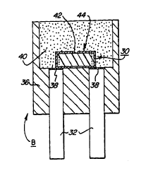
Figure 3 shows a surface-connectable SCB 30 in accordance with an embodi-
ment of the present invention. SCB 30 is also provided with unbiased
protection
against electrostatic discharge according to a particular optional aspect of
the present
invention and is shown being utilized as part of an explosives igniter B
wherein SCB
30 is attached, i.e., is surface-connected, to leads 32 of header 36 by solder
joints 38.
An explosive load 40 is in contact with active area 42a, which is formed in
the gap
between lands 44. As seen in Figure 4, SCB 30 comprises a silicon dioxide
layer 48
disposed on a p-type silicon substrate 50. A polysilicon film 52 is disposed
on por-
tions of the silicon dioxide layer 48. On either side of SCB 30, dopant
impurities 54
are introduced into the p-type silicon substrate 50. (In an alternate
embodiment, the
substrate 50 may consist of an n-type silicon substrate and the dopant
impurities 54
may consist of p-type dopant impurities.) The metal lands 44 extend along the
exte-
rior top surface of substrate 50 and are connected by electrical connector 45a
to con-
tact lands 47 on the back surface of substrate 50. The dopant impurities 54
adjacent
the lands 44 establishes back-to-back diodes 46a and 46b, which provide
unbiased
electrostatic discharge protection to SCB 30. In other words, SCB 30 includes
elec-
trostatic discharge protection regardless of the polarity of the connections
to leads 32.
The electrostatic discharge protection provided by the back-to-back diodes is
not
needed in every case, but provides protection for smaller semiconductor
elements and
in applications, such as initiation of explosives, where such added protection
is war-
ranted.
CA 02274167 1999-06-07
WO 98/28792 PCT/US97I22426
- 10 -
Figure 4A shows the schematic diagram of Figure 4 related to the structure of
SCB 30 wherein back-to-back diodes 46a, 46b are connected in parallel to the
resis-
tance provided by active area 42a. When a voltage is supplied to SCB 30
through
leads 32, most of the current will initially flow through the active area 42a
of SCB 30
until the diodes reach their intrinsic breakdown voltage, at which time
current will
flow to the zener diodes 46a, 46b. For very high spikes of voltage, as are
encountered
by electrostatic discharge, the diodes 46a, 46b will beak down and shunt the
current
therethrough, thereby decreasing the amount of current flow through active
area 42 a
of SCB 30.
The circuitry for the semiconductor bridge according to the invention is manu-
factured with standard techniques from a standard silicon substrate, commonly
re-
ferred to as a wafer or wafer substrate. While the silicon substrate has no
preferred
crystal orientation, the background substrate concentration is preferably in
the range
101' to 1018 cm3 and is optionally doped with suitable impurities to isolate
the sub-
strate's resistance, as explained below.
The fabrication process is then followed by creating the active elements or
cir-
cuits on the silicon substrate in such a way that the electrical contact pads
or layers are
extended continuously from one to the opposite side of the chip. Even though
the sur-
face mounting technique of the present invention applies to many circuit or
element
configurations such as diodes, transistors, resistors, capacitors, and any
other discrete
semiconductor component with two or three terminals, the following discussion
will
refer, by way of illustration, to SCBs. SCB technology relies on the use of
thin films
(mono-and poly-crystalline silicon) that are electrically isolated from their
substrates
by means of dielectric or non-conductive layers.
The fabrication of surface-connectable SCB elements, in accordance with the
present invention, may, for example, start with p-type, high resistivity (0.01
to 10
ohm-cm) silicon substrates that are coated on the front and on the back with a
dielec-
tric layer, typically from 0.2-1.0 micrometers thick, on which a polysilicon
film, typi-
cally 1.0-3.0 micrometers thick, is deposited by techniques well-known by
those
skilled in the art. For example, the polysilicon film deposition may be
carried out by
low pressure chemical vapor deposition of polysilicon on silicon dioxide films
that are
thermally grown on the silicon substrate at high temperatures in a controlled
oxygen-
water steam atmosphere.
CA 02274167 1999-06-07
WO 98128792 PCT/US97/22426
- 11 -
Next, the silicon substrates are subjected to the hole-, groove-, or channel-
making process, as follows. In one approach, laser drilling of holes can be
done at
selective locations on the substrate with at least a pair of holes for every
element on
the wafer. In another approach, chemical etching of grooves on the silicon
substrate
can also be done at selective locations on the wafer with at least one groove
separating
two adjacent elements. In another approach, channels and stripes can be added
by
saw-dicing of the wafer creating cuts in only one direction and all the way
through,
but not all the way across, so as to define an array of parallel strips
supported by a pe-
ripheral edge portion of the wafer.
In a preferred approach in accordance with an aspect of the present invention,
a saw dicing technique is used to cut in the wafer substrate openings which
define
between them areas of the substrate which form dies which are subsequently,
after
formation of the required circuitry thereon, cut from the wafer to provide a
plurality of
semiconductor elements from a single wafer substrate. The cutting technique em-
ployed in accordance with the invention forms square through-holes (which
extend
through the entire depth of the wafer and any coatings thereon) fi-om the
front surface
to the back surface of the wafer. The through-holes are formed by cutting the
wafer
partially through on the front surface and on the back surface, with the front
surface
cuts extending transversely, e.g., perpendicularly, to the back surface cuts.
Both cuts
are deep enough, e.g., each may extend through more than one-half the
thickness of
the wafer, such that they form squared holes at their intersections and
thereby provide
a plurality of passages which extend from the front to the back of the wafer.
Both the
back surface and front surface cuts or grooves are made wide enough so that
the sub-
sequent cutting of the wafer to separate the semiconductor elements therefrom
can be
carried out with a thinner dicing saw which will leave intact and unscathed
the side-
walls formed by the initial front surface and back surface cuts.
Referring now to Figures 5, 5A, 5B and 5C, a wafer substrate 56 is shown in
schematic view, and greatly enlarged in thickness for purposes of
illustration. Figure
5 shows the front surface 58 in plan view, having a series of parallel,
equally spaced-
apart front surface grooves 60 cut therein. As seen in Figure 5B, front
surface grooves
60 extend for slightly more than half the depth d of wafer substrate 56.
Figure 5A
shows back surface 62 of wafer substrate 56, which has a series of parallel,
equally
spaced-apart back surface grooves 64 formed therein. Back surface grooves 64,
as
CA 02274167 1999-06-07
WO 98/28792 PCT/US97122426
- 12 -
best seen in Figure 5C, are substantially equal in depth to front surface
grooves 60 and
extend for slightly more than one-half the depth d of wafer substrate 56.
The intersections of front surface grooves 60 and back surface grooves 64 re
sult in a plurality of square openings (unnumbered) formed by the
intersections of the
various grooves, and provide access between the walls 60a (only one of which
is
shown in Figure SC) defining front surface grooves 60 and the walls 64a
defining
back surface grooves 64. Respective portions of walls 60a, 64a comprise the
side sur-
faces (66a-66c and 68a-68b in, respectively, Figures 6D and 6E) of the
elements to be
cut from wafer substrate 56. Consequently, a flow path is provided as
indicated by
the unnumbered curved arrows in Figure SC for the gaseous reactant utilized in
a
gaseous thermal diffusion process to dope front surface 58, the walls of front
surface
grooves 60, the walls of back surface grooves 64, and back surface 62.
When the thermal diffusion process and other processing steps necessary are
completed, saw cuts are extended through the entire thickness of wafer
substrate 56 to
form a plurality of dies on which the appropriate SCB circuitry has been
formed to
provide a plurality of SCB elements. By using the illustrated technique, the
wafer
substrate 56 maintains its physical integrity and the processing steps may be
carried
out on the full wafer.
When it is desired to form back-to-back zener diodes on the dies, the p-doped
silicon substrate is, after the formation of openings therein, preferably by
the cross-
cutting technique illustrated in Figures 5-SC, subjected to an n-type gaseous
thermal
diffusion process, for example, one using phosphorus oxychloride (POCl3).
Phospho-
rus oxychloride provides a gaseous source of phosphorus impurities upon
reacting
with oxygen and nitrogen supplied in appropriate proportions at high
temperature.
The flow path of the phosphorus oxychloride is illustrated by the unnumbered
curved
arrows in Figure SC, as described above. The front and back polysilicon layer
and the
eventual side surfaces of the silicon substrate of every die on the wafer is
thus doped
by the gaseous diffusion process. The use of a gaseous diffusion process is
demanded
by the requirement of having continuous electrically conductive paths
established
from the front to the back surface by means of the side surfaces through the
holes,
channels or grooves formed in the wafer. It will also be appreciated that by
doping
the side surfaces of the silicon dies with n-type impurities, electrical
isolation between
the tlvo opposite side walls of every die is achieved by defining back-to-back
diodes
CA 02274167 1999-06-07
z
WO 98!28792 PCT/US97/22426
- 13 -
(when a p-type silicon substrate is used as mentioned above) that can be used
as elec-
trical components to protect the surface-connectable SCB from the effects of
electro-
static discharges.
In another aspect of the present invention, an n-type silicon substrate and a
p-
type gaseous thermal diffusion process can also be used to provide the
electrical iso-
lation between the two opposite side walls of evcry die. This is achieved by
providing
the intrinsic back-to-back zener diodes to protect the surface-connectable SCB
from
the effects of electrostatic discharges.
Both the silicon substrate and the doping gaseous source can, in accordance
with another embodiment of the present invention, be selected to be of the
same type,
either p- or n-type, to provide the continuous electrically conductive paths
needed to
connect the front and back surfaces of the dies. However, the electrical
isolation be-
tween the two opposite sides of every die is then not achieved (back-to-back
diodes
are not formed in this way) since only a simple resistive path is obtained
which, under
the right circumstances, can be intentionally designed to be of very high
resistance,
depending upon the doping level of the starting silicon substrate. It will be
appreci-
ated by those skilled in the art that this latter scenario will not provide
elements which
protect against electrostatic discharge.
In any case, after removing the excess of dopant left (namely phosphorus-
silicate glass or PSG) during the diffusion process with a buffered oxide
etching solu-
tion, a first metal layer consisting of aluminum, tungsten or any other
suitable metal,
is deposited on the front and back side of the polysilicon wafer by any
suitable stan-
dard deposition technique, for example, thermal evaporation, sputtering, etc.
During
the metal depositions the wafers are rotated in a planetary-type system so as
to expose
to the metal being deposited as much surface area of the wafer as possible.
This rota-
tional effect helps to overcome the effect on metal deposition of "shadows"
cast by
nearby structures and promotes the formation of thick and uniform metal
coatings on
the side walls of the substrate. The width of the groove and channel, as well
as the
diameter of the hole, influences the quality of the side metalization layer.
As will be appreciated by those skilled in the art, if a chemical vapor deposi-
tion technique is used to metalize the wafer with tungsten, aluminum, copper
or the
like, then the need to rotate the wafers is eliminated as a more conformable
deposition
is achieved.
CA 02274167 1999-06-07
WO 98/28792 PCT/US97/22426
- 19 -
Photo-lithography techniques and specially designed photographic plates,
well-known to those skilled in the art, are used to transfer images onto the
silicon
substrates at selected areas to create a mask that protects those selected
areas against
chemical etching agents. Etching and washing techniques are then carried out
so as to
define specific geometries on the silicon substrates. In particular, etching
and wash-
ing of aluminum and polysilicon is carried out to define the SCB geometry on
the
front surface.and to separate the metal contacts on the back surface of the
wafer. The
back side of the wafer is protected (e.g., with photo-resist) against chemical
etchants
during the etching of aluminum and polysilicon on the front surface, and vice
versa.
When the metal layer comprises aluminum, thermal treatment of the wafers is
then performed at 450°C for 30 minutes in a nitrogen atmosphere to
anneal the alumi-
num metal-semiconductor interface in order to ensure a low contact resistance
and
proper adhesion of the metal to the semiconductor.
A third photo-lithography step is carried out to mask those areas on the back
surface of the wafer with photo-resist where aluminum and polysilicon were
etched
and washed. With the photo-resist mask in place, a second metal layer that is
suitable
for soldering purposes, for example, silver, nickel, tin, gold, copper, etc.,
is laid down
by thermal evaporation, sputtering, eiectropiating, paint-on, or any other
suitable
technique on the back side of the wafer to an adequate thickness, usually from
1 to 10
micrometers. In particular, a titanium-gold layer with thickness of about 300
Ang-
stroms of Ti and 1.0 micrometer of gold was deposited on the surface-
connectable
SCB elements of one embodiment of the present invention. The titanium acts as
a
binding layer between the aluminum and gold layers, thus enhancing the
adherence of
the gold film and improving the heat transfer efficiency during the soldering
process.
During the deposition of this second metal layer on the back side surface, the
front
surface of the wafer (where the active area of the SCB has been defined) is
protected,
for example, with photo-resist, to avoid metal deposition on the bridge area.
Removal of the photo-resist mask proceeds by the lift-off technique which re-
moves the metal on it. In this way the titanium-gold layer stays only on the
alumi-
num/polysilicon pads previously described.
The wafer is then taken to an electrical testing station where resistance of
every SCB element is checked. The appearance of the die is also inspected
under a
CA 02274167 1999-06-07
WO 98128792 PCT/US97/22426
- 15 -
microscope. Electrically and visually bad dies are marked and subsequently dis-
carded.
Finally, the wafers are cut with a dicing saw which is thinner than that used
to
cut the front surface grooves 60 and back surface grooves 64 in order to
separate the
individual SCB elements from the wafer and tom each other. This time the
dicing
cuts are passed entirely through the wafer to separate rows and columns of
dies as
previously defined by the location of the apertures.
Figures 6 through 6E illustrate SCB 30, shown schematically in Figure 4, in
somewhat more detail. SCB 30, as illustrated in Figures 6-6E, is a typical
product of
the above-described process of manufacturing a plurality of silicon
semiconductor
elements from a wafer, as illustrated in Figures 5-SC. The components of SCB
30
which are illustrated in Figure 4 are identically numbered in Figures 6-6E,
and the de-
scription thereof is not repeated.
Figure 6 shows a plan view and Figure 6D a perspective view of the top sur-
face 34 of SCB 30; Figure 6E shows the bottom surface 3~ of SCB 30. SCB 30 com-
prises an electrically non-conducting substrate 50 which, as is well known in
the art,
may comprise any suitable electrically non-conducting material and may
comprise a
monocrystalline silicon substrate. As described, for example, in the
aforementioned
U.S. Patent 4,708,060 of R.W. Bickes, Jr. et al, metaliized lands 44 formed in
the
configuration illustrated in Figure 6 and 6D overlie a semiconductor material,
such as
a heavily doped silicon semiconductor 42. The latter is disposed upon
substrate ~0 in
a "bow tie" configuration comprising two pads of relatively large surface area
(overlain by metal lands 44) and a small bride or active layer 42 a connecting
the two
large pads. A similar structure is shown in co-pending patent application
serial num-
ber 08/644,008 of Bernardo Martinez-Tovar et al entitled "Semiconductor Bridge
Element and Method of Making the Same".
When an electric potential is applied across lands 44, the active area 42a of
semiconductor layer 42 becomes conducting and when a current of sufficient
intensity
is applied for a sufficient length of time, active area 42a erupts with the
formation of a
plasma, which will serve to provide a heat source for use in, e.~., initiating
explosive
materials packed in contact with active area 42a. SCB 30, as best seen in
Figures 6A,
6B, 6D and 6E, is of stepped configuration at the sides. This stepped
structure results
from the fact that SCB 30 has been prepared by a method as illustrated in
Figures ~-
CA 02274167 1999-06-07
WO 98/28792 PCT/US97/22426
- 16 -
SC, in which front surface grooves 60 and back surface grooves 64 are cut with
dicing
saws, which are wider than the dicing saws subsequently used to separate the
individ-
ual SCBs. Thus, in Figure 5B, a relatively thin dicing saw is positioned
midway
along the width of front surface grooves 60, for example, along line C-C in
Figure 5B,
to cut through the wafer to separate the individual semiconductor elements
therefrom.
Corresponding thin-blade cuts are made along each of front surface grooves 60
and
back surface grooves 64 to separate the individual semiconductor elements from
the
wafer substrate 56 and from each other. As explained above, because front
surface
grooves 60 and back surface grooves 64 intersect, through-holes or apertures
(unnumbered) are formed in the wafer substrate 56 and provide a path for
deposition
of metals and dopants. Consequently, upon deposition such as chemical vapor
depo-
sition of the metal which forms metal lands 44, the metal is also deposited on
the side
surfaces 66a, 66b and 66c (Figure 6E). Side surface 66b is seen to be a ledge
or pro-
jection between side surfaces 66a and 66c. Side surface 66b is a longitudinal
segment
of the bottom of a front or back surface groove, and side surface 66c is made
by the
cut of the relatively thin dicing saw.
A similar procedure results in the stepped configuration of side surfaces 68a,
68b, 68c, which extend transversely to side surfaces 66a, 66b, 66c. (In
Figures 6D
anii oc, small portions of the metal layer overlying the side surfaces are
broken away
for clarity of illustration.)
The through-holes or apertures formed in wafer substrate 56 (Figures 5-5C)
provide, as illustrated in Figure 5C, a pathway for deposition of metal by,
e.g., a
chemical vapor deposition process, so that the metal layer forming lands 44
extends
continuously to provide electrical connectors 45a, 45b, 45c, which serve to
connect
metal lands 44 with contact lands 47 (Figure 6E). In Figures 6D and 6E
connectors
45a and 45b are shown partially broken away in order to show a portion of side
walls
68a and 68b. Contact lands 47 are covered by a layer of bonding metal 49, in
order to
promote effective and efficient soldering of the SCB 30 to a header 36 as
illustrated in
Figure 3.
The bonding metal 49 may comprise gold or other suitable metal such as
nickel or silver, in order to provide higher quality solder joints 38 (Figure
3).
A continuous metal layer is seen to provide lands 44, connectors 45a, 45b and
=~5c and contact lands 47, thereby providing a continuous electrically
conductive path
CA 02274167 1999-06-07
WO 98/28792 PCT/US97122426 ?
7 _ _
on SCB 30 extending from the front surface 34 along the side surfaces 66a, 66b
and
66c and 68a, 68b and 68c, thence to the rear surface 35. The resulting
structure of
flat, planar contact lands 47, optionally overlain by a thin layer of bonding
metal 49,
provides electrical contacts which are dimensioned and conf gored to be
electrically
connected by being directly mounted upon a header, and soldered or otherwise
con-
nected to electrical contacts in a manner such as that illustrated in Figure
3, wherein
solder 38 connects the back surface of the SCB 30 to electrical leads 32.
While the invention has been described in detail with reference to specific em-
bodiments thereof, it will be appreciated that numerous variations thereto
will none-
theless lie within the scope of the appended claims.