Note: Descriptions are shown in the official language in which they were submitted.
' CA 02274176 1999-0-6-08
. ''
1
A TAPERED RIB WAVEGUIDE
TECHNICAL FIELD
This invention relates to a tapered rib waveguide providing a transition from
an
optical waveguide of relatively large cross-section to an optical waveguide of
smaller cross-section.
BACKGROUND ART
An integrated optical circuit employs optical waveguides to transmit light
around
the circuit and to connect to external optical waveguides such as optical
fibres.
The integrated optical waveguides and/or optical fibres may be of different
cross-sectional size so there is a need for means to provide a transition from
a
waveguide of relatively large cross-section to a waveguide of smaller cross-
section. A variety of devices have been proposed for this purpose but they
tend
to be relatively complex and/or difficult to fabricate.
US-A-5078516 discloses a single-mode tapered rib waveguide comprising a
low-index substrate and a high index rib. In the wide portion of the rib, the
optical power is concentrated in the rib and in the narrow portion, the
optical
power is more loosely conned in the substrate.
This invention aims to provide a tapered rib waveguide which is of relatively
simple construction) is relatively easy to fabricate and which provides a low-
loss
transition from a large cross-section to a smaller cross-section.
It should be noted that terms such as "upper", "lower", "laterally" etc. used
herein are used in a relative sense, i.e. relative to the orientation of the '
apparatus shown in the accompanying drawing, and are not intended to imply
any orientation with respect to the force of gravity.
AMENDED SHEET
..r........ ._......._.. _.. ,.. _. CA 02274176 1999-06-08 . _ ... _
;, _
-, ~ ~ . , .
2
DISCLOSURE OF INVENTION
According to a first aspect of the present invention, there is provided a
tapered
rib waveguide tapering from a large, multi-mode optical waveguide to a
smaller,
single-mode optical waveguide, the tapered rib waveguide comprising at least
two portions formed of the same material: a lower portion which tapers inwards
laterally in the direction from the large waveguide to the smaller waveguide
and
an upper portion, formed on the lower portion, which tapers inwards to a point
or other form of termination in the direction from the large waveguide to the
smaller waveguide) the dimensions of the two portions being arranged such
that substantially all of a fundamental mode propagated in the large multi-
mode
waveguide is coupled to the smaller, single-mode waveguide.
Preferred features of the invention will be apparent from the subsidiary
claims
of the specification and from the following description.
BRIEF DESCRIPTION OF DRAWINGS
The invention will now be further described, merely by way of example, with
reference to the accompanying drawings in which
Figure 1 shows a perspective view of a preferred embodiment of a tapered rib
waveguide according to the invention,
Figure 2A is a schematic plan view of another embodiment of a tapered rib
waveguide according to the invention, and Figure 2B a cross-section thereof;
and
Figures 3A and 3B, 4A and 4B, and 5A and 5B show schematic plan and side '
views of three further embodiments of a tapered rib waveguide according to the
invention.
AMENDED SHEET
CA 02274176 1999-06-08
WO 98/35250 PCT/GB98/00384
3
in Very Large Scale Integration (VSLI) electronic circuits. The paper "Reduced
defect density in silicon-on-insulator structures formed by oxygen
implantation
in two steps" by J. Morgail et al. Appl. Phys. Lett, 54, p526,1989 describes
the
manufacture of suitable wafers. Methods of manufacturing rib waveguides on a
. silicon-on-insulator chip are described in the paper "Low loss single mode
optical waveguides with large cross-section in silicon-on-insulator" by J.
Schmidtchen et al, Electronic Letters, 27,p1486,1991.
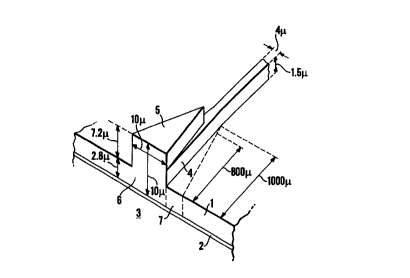
The drawing shows the rib waveguides formed in the silicon layer 1 of such a
chip and shows the oxide layer 2 separating the silicon layer 1 from a silicon
substrate 3. A silicon dioxide cladding (not shown) is also usually provided
over the rib.
The tapered rib waveguide shown in the drawing comprises two portions: a
lower portion 4 which tapers laterally from a width of about 10 microns to a
width of about 4 microns over a length of about 1000 microns, and an upper
portion 5, formed on the lower portion 4, which tapers from a width of about
10
microns to a point over a length of about 800 microns. The upper portion 5
thus tapers more rapidly than the lower portion 4 and in the embodiment shown
has a triangular. wedge-like shape when viewed from above. Both portions
are, however, designed to provide a substantially adiabatic taper.
In another arrangement (not shown), both the upper and lower portions 5 and 4
taper at the same angle so the sides of the two portions are parallel to each
other. In this case) the wide end of the upper portion 5 is narrower than the
wide end of the lower portion 4
The upper and lower portions 5 and 4 preferably taper at an angle (with
respect
to the axis of the waveguide) of less than 1 degree and preferably less than
0.5
of a degree. Such a gradual taper ensures that any losses caused by the taper
are kept small. The upper portion 4 tapers to a point or to some other form of
CA 02274176 1999-06-08
WO 98/35250 PCT/GB9$/00384
4
termination. In the arrangement shown in Figure 1, the tapering section of the
upper portion 5 is formed on top of the tapering section of the lower portion
4.
The two portions 4 and 5; including the input facet 6, can be formed together
by
conventional lithography and dry etching as they are defined by vertical
surfaces. They are formed of the same material and thus have the same
refractive index. The two portions may be formed homogenously on the chip.
Alternatively, the upper portion 5 may be formed separately and mounted on
the lower portion 4.
The upper faces of the upper and lower portions 4 and 5 are substantially
parallel to the plane of the chip, i.e. the upper and lower portions 4 and 5
each
have a substantially constant height above the surface of the chip (7.2 and
1.5
microns. respectively, in the illustrated example).
The tapered rib waveguide shown in the drawing thus provides a two-
dimensional taper, the taper in the lateral direction being provided by an
actual
tapering of the waveguide and the taper in the vertical direction (i.e.
perpendicular to the plane of the chip) being provided by means of the
laterally
tapered upper portion 5. The problems associated with forming a vertically
tapered waveguide, i.e. defined by non-vertical surfaces, as used in some of
the prior art. are thus avoided.
The shape and dimensions of the tapered rib waveguide are such that if the
large. multi-mode waveguide is excited in a fundamental mode only, this mode
is forced down into the smaller. single-mode waveguide as the cross-sectional
shape of the waveguide changes gradually from that of the larger waveguide to
that of the smaller waveguide. The effective refractive index in the upper
portion 5 is progressively reduced as it tapers. This forces the mode into the
lower portion 4 of the waveguide. It should be noted that the tapered rib
waveguide does not require a refractive index difference between the two
CA 02274176 1999-06-08
WO 98/35250 PCT/GB98/00384
portions or for the maintenance of single-mode operation of the larger
waveguide. As indicated above, the larger 10 micron x 10 micron waveguide is
a multi-mode waveguide but if it is excited by a fundamental mode on its axis,
e.g. from an optical fibre. the power in higher order modes is negligible.
The large refractive index difference between the silicon waveguide and the
silicon dioxide cladding (not shown) helps ensure that the effective
refractive
index of the upper portion 5 is suppressed sufficiently for the optical mode
to be
substantially entirely guided into the lower portion 4 before the narrowest
section thereof is reached. Thus, as indicated above, the upper portion 5 need
not taper to a point so the difficulties of fabricating very narrow sections
at the
narrow end of the upper portion 5 can be avoided.
The dimensions of the two portions 4 and 5 are selected in accordance with
conventional requirements of rib waveguides and with appropriate dimensions
substantially all of a fundamental mode propagated in the large multi-mode
waveguide is coupled to the smaller, single-mode waveguide.
A typical example having dimensions as shown in the drawing provides a low-
loss coupling (typically 0.1 dB or less) between the two waveguides.
The tapered rib waveguide described herein may be used to provide a
transition between a variety of sizes of waveguide and particularly from an
optical fibre to a smaller integrated waveguide. The larger waveguide
typically
has cross-sectional dimensions in the range 7 - 12 microns wide by 7 - 12
microns deep (and is thus compatible with conventional optical fibres) and the
smaller waveguide typically has cross-sectional dimensions in the range 2 - 5
~ microns wide by 4 - 5 microns deep (and is thus compatible with conventional
integrated optical waveguides). As shown in Figure 1, the depth is measured
from the oxide layer 2.
CA 02274176 1999-06-08
WO 98/35250 PCT/GB98/00384
6
As indicated above. the input facet 6 may be formed by dry etching, no saw
cuts or polishing being necessary. The facet 6 may be perpendicular to the
axis of the waveguide or may be angled.
It will also be appreciated that the tapered rib waveguide can be used in
either
direction, i.e. from a large waveguide to a small waveguide or from a small
waveguide to a large waveguide.
The tapered rib waveguide described above is easily integrated With other
components of an integrated optical circuit. An optical fibre (not shown)
inputting light into facet 6 may be positioned in a V-groove (not shown)
provided in the silicon-on-insulator chip. The position of the V-groove and of
the tapered rib waveguide may be defined by a common lithographic step so
they are automatically aligned with each other.
The applicants' co-pending application no. PCTlGB9F101068 (Publication no.
W097/45234) describes a connection between an integrated optical
waveguide and an optical fibre and is hereby incorporated herein. This earlier
application describes a rib waveguide formed on a silicon-on-insulator chip.
the
rib waveguide and underlying layer of silicon dioxide overhanging the end of a
V-groove formed in the chip in which an optical fibre is positioned so the end
of
the rib waveguide lies in close proximity with the end of the optical fibre,
the
overhang being required as the end of the V-groove is not formed
perpendicular to the surface of the chip.
The tapered rib waveguide structure described herein may be formed on such
an overhang to provide a transition between a large, multi-mode waveguide for
receiving light from the optical fibre and a smaller, single-mode integrated
waveguide formed on the chip.
CA 02274176 1999-06-08
WO 98/35250 PCT/GB98/00384
7
The illustrated embodiment comprises a tapered rib waveguide formed as a
straight waveguide. In some circumstances, however, it may be desirable to
form a similar structure on a gradually curving waveguide. The tapered sides
of the upper and lower portions 4 and 5 do not need to be straight but may
also
be curved, nor need they necessarily be symmetrical.
As indicated above, the taper should be gradual. If the taper is too rapid.
the
losses will be higher. On the other hand. if the taper is too gradual. the
device
may be larger than is desirable. A compromise between these two
requirements is usually necessary.
In addition to tapering the lower portion 4, a tapered section of the silicon
slab
7 may also be removed as shown by dashed lines in Figure 1. Removal of the
slab 7 adjacent the rib waveguide increases the refractive index difference
between the waveguide and its surroundings and by gradually narrowing the
gap 7) the effective refractive index difference is gradually reduced.
The illustrated embodiment shows a tapered waveguide having two layers. i.e.
the upper portion 5 and lower portion 4. However, it will be appreciated that
further layers may be provided, e.g. an additional tapering portion on top of
the
upper portion 5, and that the tapering may occur in two or more stages at
different positions along the waveguide.
Figures 2A and 2B are schematic diagrams illustrating an example of a multi-
stage tapered rib waveguide. A 10 microns high rib 10 initially tapers to a 7
microns high rib 11 which then tapers to a 4 microns high rib 12. Figure 2B
shows a cross-section taken across line a-a of Figure 2A. By this means a 10 x
microns waveguide can be tapered down in two stages to a 2 x 4 microns
waveguide, e.g. for coupling with a laser. The tapered portion 10 overlaps the
tapered portion 11 so as to reduce or minimise losses due to light diverging
as
CA 02274176 1999-06-08
WO 98/35250 PCT/GB98/00384
8
it is forced down from portion 10 to portion 11 and, similarly, tapered
portion 11
overlaps tapered portion 12.
Figures 3 - 5 show further embodiments of a tapered waveguide,
The arrangement shown in Figures 3A and 3B is similar to that shown in Figure
1 except that the tapered structure 13, comprising the upper and lower
portions
and 4 and a substrate 14 on which these are formed, is a separate
component which is mounted on a silicon-on-insulator chip 15 and aligned with
a waveguide 16 thereon. This enables the tapered structure 13 to be formed of
a different material. e.g. silicon dioxide or silicon nitride, and enables it
to be
fabricated separately from the remainder of the optical circuit.
The tapered structure 13 is mounted on the silicon-on-insulator chip 15 by
locating surfaces 13A and 13B against corresponding surfaces 15A and 15B in
a recess or cut-out section of the chip 15. A further pair of abutting
surfaces
(not shown) may be provided for locating it in a lateral direction relative to
the
waveguide 16. The tapered structure 13 may be secured in place by means of
adhesive.
A two-stage tapered waveguide may also be made in a similar manner as
shown in Figures 4A and 4B. In this case, a separate tapered structure 17 is
provided which comprises the upper tapered. portion 5 on an untapered portion
18 and a substrate 19. The lower tapered portion 4 is formed on the silicon-on-
insulator chip 15. The tapered structure 17 is mounted on and aligned with the
silicon-on-insulator chip 15 in a similar manner to that described above.
Figures 5A and 5B show a further arrangement in which a tapered structure 20
of a different material is fabricated directly onto a silicon-on-insulator
chip 15.
Figures 5A and 5B are similar to Figures 3A and 3B but in this case the upper
and lower portions 5 and 4 and substrate 14 are fabricated directly onto the
CA 02274176 1999-06-08
WO 98/35250 PCT/GB98/00384
9
chip 15. The tapered structure 20 may, for example, be formed of silicon
dioxide deposited or grown on the silicon-on-insulator chip 15 or formed of a
polymer material spun onto the chip.
As the tapered structures 13, 17 and 20 are formed of a different material
compared to the waveguide 16 (and lower portion 4 in Figure 4), an anti-
reflective coating is preferably provided between the two to help reduce back-
reflection of light passing from the tapered structure into the silicon-on-
insulator
device.
Although the examples described above are formed on a silicon-on-insulator
chip. and although this has the advantages referred to above, a similar
tapered
rib waveguide can be formed on other types of chip.