Note: Descriptions are shown in the official language in which they were submitted.
CA 02274193 1999-06-10
1
METHOD FOR MAKING INTEGRATED AND COMPOSITE OPTICAL DEVICES UTILIZING
PREFABRICATED OPTICAL FIBERS AND SUCH DEVICES
~s~ld Qf the Invention
The present invention relates generally to optical devices, and
S particularly relates to methods of making devices incorporating
prefabricated optical fibers. More particularly, the invention also
relates to integrated optic chips (IOCs) with embedded optical fibers
and carved-out regions for mounting or creating other components
therein.
Backaround of the Invention
Integrated optic chips consist of different elementary waveguide
circuits such as straight waveguides, couplers, branches, and bends.
Depending on the type of material used in fabrication of the waveguide
they can perform different functions such as light generation,
amplification, modulation, splitting and so on. One important family
of IOCs are silica-based planar integrated circuit devices that perform
mostly passive operations such as coupling, splitting and filtering.
Two exemplary methods for fabricating silica based IOCs are flame
hydrolysis and ion exchange, which yield low loss waveguide devices.
However, making waveguide grating devices in waveguides made by these
CA 02274193 1999-06-10
2
methods is difficult and expensive. Waveguide gratings are important
for providing functions such as narrow band filtering and adding,
dropping and routing wavelengths.
One attractive method for fabricating waveguide devices with gratings
is by direct creation (writing) of waveguides by illuminating with
electromagnetic radiation exposed areas in a thin film of photosensitive
material such as organically modified glasses. However, this technology
may not be suitable for mass fabrication and the waveguides made thereby
may suffer from excess propagation losses compared with commercially
entrenched waveguide fabrication techniques. Another disadvantage is
that one-stage fabrication of large area integrated optic circuits with
crowded elements is risky and results in low yield and therefore high
cost.
Prefabricated standard optical fibers are to date the best known type
of optical waveguide to guide light with very low propagation loss. It
is also possible to write gratings on optical fibers and utilize them
in all-fiber circuits with the desired functions. But a major
deficiency of all-fiber circuits is that optical fiber pieces used
either as a waveguide or a waveguide with grating are not flexible
enough to be connected together in a compact farm. Moreover, some of
the optical elements cannot be made using fibers consistently. A
desirable integrated optic technology would offer the necessary
flexibility to make some of the optical elements that are difficult to
build with fibers while also providing optical connection at the board
CA 02274193 1999-06-10
3
level utilizing the flexibility of integrated optical waveguides.
A rel fable and economic technology that can offer the advantages of both
all-fiber made devices and the flexibility of planar optical waveguides
for optical interconnection and the fabricating of those devices that
are best implemented by planar waveguides, such as branches and
couplers, is desirable. It is also desirable to have the capability of
fabricating the optical elements in successive independent stages,
possibly from different materials and with different processes.
Regardless of the fabrication method of an integrated optic circuit on
a substrate there is the problem of attaching fibers to waveguides in
an economical way. The prior art has addressed the subject of how to
attach a fiber to a waveguide. The best known method of attaching
fibers to waveguides uses etched V-grooves to position the fiber in
front of the waveguide. For instance, in United States Patent No.
5,175,781 "Attaching Optical Fibers To Integrated Optic Chips", issued
December 29, 1992 to Hockaday et al., there is disclosed a method of
attaching fiber to integrated optic chips by forming aligning grooves,
using laser ablation, on the IOC followed by cutting the surface ends
of the waveguides by a dicing saw and then disposing the optical fibers
within the grooves and securing them with adhesives to attach the fibers
to the IOC permanently. Disadvantages of such methods are that they are
labour intensive, cannot assure perfect alignment of fibers and planar
waveguides in all directions, and that they introduce excess losses due
to a mismatch between the core size of the optical fiber and the
CA 02274193 1999-06-10
4
waveguide. It is therefore also desirable to provide a method of
attaching fibers to a waveguide circuit which is less time consuming,
has lower excess loss, is more reliable, and is amenable to being
automated.
Summary of the Invention
The present invention endeavours to mitigate same of the above-mentioned
problems of IOC fabrication.
In the present invention, optical fibers are first embedded in a
substrate and are precisely placed in predetermined positions by
lithography, molding, laser, chemical or mechanical micromachining,
their positions being readable with the aid of markers on the front and
possibly back surfaces of the substrate defining a metric system for
locating the fibers precisely in both lateral directions. The fibers
are affixed in the grooves by adhesives or the like; then strips of the
IS substrate with fibers embedded therein are cut from the left and right
sides. The left and right separated sections, with the embedded fibers
and extra lengths of loose fibers protruding beyond the edges of these
sections, are end polished, if necessary, and kept for later re-
attachment to the substrate with the embedded fibers used as the
input/output connectors. The remaining section, referred to here as
"Integrated Optical Board" (IOB) when finished, is then carved to an
appropriate depth in designated areas and filled or coated (by dip
coating or other methods) with layers of suitable materials from which
CA 02274193 1999-06-10
a waveguide device can be fabricated. The waveguide will connect the
input/output fibers optically with the patterns of waveguide circuits
by using the markers to find the exact location of the embedded fibers
in the IOB. Alternatively different areas of the carved IOB can be
5 filled or coated with different materials such that the waveguide
devices made of these material will perform different functions. If
necessary, using a dicing saw, the~end faces of the embedded fibers and
the fabricated waveguides are cut and polished at an angle to reduce the
coupling losses and optical reflection from the interfaces of sections
with different refractive indexes. Having completed the optical
interconnection of the different points in the IOB, the two right and
left connectors are re-attached to the IOB by perfectly aligning the end
faces of the fibers inside the connectors and the fibers inside the IOB.
Thus, fast or automatic alignment of fibers to IOCs is achieved.
Further, fiber based devices are easily integrated with planar optical
waveguides in one substrate.
In a method aspect of the present invention an optical fiber is first
secured in a groove in the surface of an optic substrate, which is
subsequently processed to create requisite integrated optic components
in portions thereof.
After the optical fiber has been secured in the groove, opposite optic
substrate ends may be excised to serve as optical connectors to the
remaining central portion after its processing has been completed. For
CA 02274193 1999-06-10
6
convenience, the central portion, once processing has completed, is
hereafter refereed to as an integrated optic board (IOB).
In a preferred aspect of the present invention, the central portion of
a substrate, having embedded fibers therein, is processed by: polishing
or removing its top layer all down to the top of the fibers' cores;
carving out a predefined region, or regions, in its top layer down to
a depth at least exposing part of the fibers' cores; and filling or
coating the carved out region, or regions, with an optical material or
materials in one or more layers, one of which may be photosensitive, for
creating a planar optical waveguide or other optical components therein;
thereby providing an IOB interconnectable to other devices through the
embedded optical fibers.
The step of removing the top layer off may be omitted at the risk of
increasing the tolerance in the depth of the carved out region.
The method of the present invention also incorporates applying a
plurality of surface markers to the optic substrate prior to processing
for subsequent alignments.
An optical device according to the present invention comprises at least
an I OB hav i ng an i ntegrated opt i c component there i n and an embedded
optical fiber and a connector also having an embedded optical fiber
characterized in that both the IOB and the connector were excised from
the same or similar optic substrate after the optical fiber has been
CA 02274193 1999-06-10
7
embedded therein, thereby providing optimal alignment between connector
and IOB.
In another device aspect, the present invention provides an integrated
optic chip, comprising: a planar optical waveguide in at least one upper
layer region of an optic substrate; and an optical fiber fully embedded
in another upper layer region of the optic substrate and coupled at one
end thereof to one end of the planar optical waveguide.
Brief Description of the Drawin4s
The preferred embodiments of the present invention will now be described
IU in detail by way of example with reference to the accompanying drawings,
in which:
Figure 1 is a perspective view of a substrate with grooves and markers
in its surface according to the present invention;
Figure 2 is a perspective of the substrate on Figure 1 with optic fibers
IS placed in the grooves with the fiber ends protruding from opposite sides
of the substrate;
Figure 3 shows the substrate of Figure 2 having two strips cut therefrom
to form two (left and right) connectors;
Figure 4 shows the central portion of the substrate of Figure 3 after
CA 02274193 1999-06-10
a central region thereof has been carved out to accommodate optical
component;
Figure 5 shows the central portion of the substrate of Figure 3 after
two regions on either side of the centre have been carved out to
accommodate two optical components;
Figure 6 shows the substrate of Figure 4 in which the carved out region
is shown filled or coated with two layers, at least one of which being
photosensitive;
Figure 7 shows the substrate of Figure 6 with the upper layer having
l0 planar waveguides;
Figure 8 shows the substrate of Figure 7 with an upper cladding layer
covering the planar waveguide layer;
Figure 9 shows an alternative embodiment wherein the substrate of Figure
7 is further processed to provide auxiliary grooves cut between the
waveguide ends and the optical fiber ends; and
Figure 10 shows the substrate of Figure 3 wherein the top layer has been
polished (or removed) down to the top of the fibers' cores and wherein
a central portion of the substrate (or IOB) is carved out (for example,
by RIE) to just expose part of the optical fibers' cores.
CA 02274193 1999-06-10
9
Detailed Description of the Preferred Embodiments
Referring to Figure 1 of the drawings, it shows a substrate 10, four
grooves 11 along one of its dimensions in the surface thereof, and a
plurality of surface markings 12 on the surface islands on either side
of the grooves 11. Markings may also be provided on the opposite
surface of the substrate 10. Preferably, the substrate 10 is made from
phosphorous doped silica glass to facilitate etching by a solution of
hydrofluoric acid, if such is used. But, of course, other types of
substrate such as silicon, lithium niobate or other desirable materials
and other types of chemical etching or laser ablation, etc. may be used
after using well-known lithography techniques (see, for example,
"Introduction to Microelectronic Fabrication, Modular Series on Solid
State Devices," by Richard C. Jaeger, editors; Gerold W. Neubeck, Robert
F. Pierret, Addison-Wesley Publishing Company, vol. 5, 1993.).
The grooves 11 are made, for example by etching, to a depth sufficient
to firmly accommodate the fibers 13 (shown in Figure 2) inside them.
Preferably, the grooves 11 have a depth that is slightly larger than the
outer diameter of the fibers 13 in order for them to be buried
completely inside the grooves 11. In order to minimize stresses due to
differences in thermal expansion, the characteristic parameters of the
substrate 10 should be as close as possible to those of the fibers 13.
The markers 12 are necessary in order to provide optical alignment of
other components with the fibers 13.
CA 02274193 1999-06-10
Figure 2 shows the substrate 10 with the fibers 13 embedded in the
grooves 11. As may be seen in the f figure, the f fibers 13 protrude beyond
either edge of the substrate 10. After placing them in the grooves 11,
the fibers 13 are held firmly in place and completely covered with an
5 adhesive, such as sol-gel liquid glass or the like. Again the
characteristic parameters, such as thermal expansion coefficient and
refractive index, of the adhesive should be close to those of the
substrate 10 and the fibers 13. Of course, prior to applying the
adhesive, the substrate 10 is washed with a suitable chemical solvent
10 (see the above cited reference).
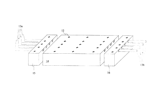
The result of the next step in the process is shown in Figure 3, where
two strips adjacent the fibers 13 ends have been cut to provide two
optical fiber connectors, the left connector 15 and the right connector
16, with fiber ends 13a and 13b protruding from the former and the
latter, respectively. The surfaces of the connectors 15 and 16 opposite
the protruding fibers 13a, 13b are polished, if necessary, and the
connectors kept for later attachment to the central portion 14, or
another similar central portion, which once processed forms the IOB.
Having excised the connectors 15 and 16 from the substrate 10, the IOB
14 is now ready far further processing. Figures 4 and 5 show two
embodiments of how to process the substrate 10 further. In Figure 4 one
central portion 17 is carved out, while in Figure 6 two portions 18 and
19, on either side of a central island 20 are carved out, and polished
such that the cut input/output fiber core ends are at least fully
CA 02274193 1999-06-10
11
exposed. The usual dicing saw is used for this step of the process, as
is normally used for cutting and polishing the end-faces of the fibers
(at the desired angle with respect to the fiber axis). However, other
methods such as wet etching or reactive ion etching (RIE) may be used
to provide the carved out portion.
Now an exemplary step of providing a planar wave-guide in the carved out
portion 17 of the I08 14 will be described with reference to Figures 6
and 7. The carved area 17 is filled or coated with layers 21 and 22 of
silica glass or other suitable and desirable material from which the
waveguide 23 circuit is going to be made. The layers 21 and 22 can be
deposited for instance using flame hydrolysis, or by filling or coating
and drying the area with layers of liquid glass such as sol-gel
solution. The mask that is used to fabricate and imprint the waveguide
23 circuitry with a group of input and output waveguides will closely
l5 match these waveguides with the embedded fibers 13 using the markers 12.
The input/output waveguide distances are standard and equal to the
distance of the embedded fibers. Markers 12 ensure that the input/out
waveguides are aligned with the embedded fibers. As shown in Figure 8
a third or upper cladding layer 26 may be provided on top of the middle
layer 22 before or after the waveguides 23 have been made. Two example
methods of fabricating waveguides in the carved out areas 17, 18 and 19
are given below.
The first method uses flame hydrolysis to deposit a layer 21 of silica
glass on the carved out area as a lower cladding followed by depositing
CA 02274193 1999-06-10
12
another layer 22 with slightly higher refractive index as the core
layer. Flame hydrolysis deposition has been described for example in
"Optical Fiber Communications," John M. Senior, Prentice Hall
International Series, Ch.4, 1992. The surface level and thickness of
the cladding and core layer are adjusted to align and match the core
layer with the core region of the embedded fibers 13 in order to
minimize the coupling loss. The waveguide 23 circuit is then fabricated
by lithography and reactive ion etching or any other suitable method.
Using the markers 12 ensures the optical alignment of the waveguides 23
axis with the embedded fiber 13 axis by aligning the markers on the
waveguide circuitry mask with the pre-imprinted standard markers 12 on
either side of the IOB 14. After fabricating the waveguide 23, an upper
cladding layer 26 (as shown in Figure 8) may also be deposited on the
waveguides to shape the mode field as close as possible to that of the
fiber. For example, the waveguide core could be 8 microns wide with the
index difference between the cladding layer and the care layer about
0.28 percent; while the fibers would be single mode fibers with 125
micron outer diameter and 9 micron core diameter.
In another example method of fabricating waveguides the carved area 17
is filled or coated with layers of sol-gel solution for lower cladding,
core, and upper cladding. Sol-gel glass is a liquid solution form of
an organically modified glass from which one can make thin or thick
layers of glass after drying the sol-gel. One convenient method of
fabricating waveguides using sol-gel is direct writing of the waveguide
by a contact mask on a photosensitive sol-gel containing photo
CA 02274193 1999-06-10
13
initiators. However, one can also use other techniques such as etching
to fabricate ridge waveguides and then cover them with a cladding layer.
Different techniques of fabricating optical waveguides have been
described, for instance, in the article "Fabrication and
Characterization of Low-Loss, Sol-Gel Planar Waveguides", Anal. Chem,
pp. 1254-1263, Vol. 66, 1994; and in another article "Ultraviolet light
imprinted sol-gel silica glass channel waveguides on silicon", SPIE, 38-
41, vol. 2695, 1996. The carved area 17 may be filled or coated with
a non-photosensitive sol-gel and then dried with the associated drying
method as the lower cladding 21. This is followed by depositing another
layer of sol-gel as the core layer 22. The core layer 22 might be
photosensitive in which case its refractive index will increase upon
exposing to certain electromagnetic radiation such as ultraviolet (UV)
radiation. The surface level and thickness of the cladding and core
layers 21 and 22 are adjusted to align and match the core layer with the
core region of the embedded fiber 13 in order to minimize the coupling
loss. The mask carrying the waveguide circuitry will then be aligned
w i th respect to the markers 12 to ensure the automat i c opt i ca 1 a 1 i
gnment
of the fabricated waveguide to the embedded fibers. This requires a
mask which has openings corresponding to a number of the markers 12 and
the pattern of the waveguide 23 in alignment with the input/output group
of fibers 13. The waveguide is fabricated either by UV imprinting or
other suitable methods in the layer of the photo-sensitive sol-gel such
that the mask's markers are in full alignment with those (12) already
imprinted on the substrate 10. Preferably another layer of sol-gel
glass will cover the waveguide as the upper cladding layer 26 in Figure
CA 02274193 1999-06-10
14
8. Referring back to Figure 5 in particular, each of the two carved
areas 18 and 19, can be used independently to fabricate a waveguide
circuitry according to the above described methods. For instance, the
fibers in the island 20 may be used as arms of a Mach-Zhender
interferometer. It is also possible to fabricate a grating on these
embedded fibers in a Mach-Zhender configuration to achieve a multiple
add/drop device. In addition, the materials and the fabrication
technologies that are used for each carved area can be different. Those
skilled in the art can easily adapt other fabrication methods of
waveguide circuitry, or use other materials and architectures different
from the present invention without departing from the scope thereof.
Referring now to Figure 9, it shows an embodiment of the invention
wherein after fabrication of the waveguides 23 a dicing saw is used to
make an auxiliary groove 24 almost perpendicular to the waveguide and
fiber axes in order to remove imperfectly fabricated parts of the
waveguide circuit in areas immediately adjoining the embedded fibers.
{A dicing saw will also polish the end faces of the waveguides and
f i tiers . ) The aux i 1 i ary groove 24 may or may not be f i 11 ed wi th an
i ndex
matching material.
Figure 10 shows an embodiment wherein the top layer of the IOB 14 has
been polished (or otherwise removed) such that the cores of the fibers
are just exposed and where the central portion 17 has being carved out,
using RIE (reactive ion etching) or other suitable methods, to expose,
in cross-section, at least part of the fibers' 13 cores 25, such that
CA 02274193 1999-06-10
the depth of the carved out portion is about the core diameter. This
is useful since it enables control of the depth of the carved area very
well using RIE. In this way the carved area is filled or coated with
only one layer, while the depth of the carved area is precisely
5 controlled. This method decreases the uncertainty when it is required
to fill or coat the carved area to an exact thickness with the desired
material.