Note: Descriptions are shown in the official language in which they were submitted.
CA 02274335 1999-06-11
-- 1 -
OSCILLATOR MODULE AND COMMUNICATIONS DEVICE USING THE SAME
BACKGROUND OF THE INVENTION
1. Field of the Invention
The present invention relates to an oscillator module
and a communications device using the same and, more
particularly, to an oscillator module used in an ultra-low
power or low-power radio device, and a communications device
using the same.
2. Description of the Related Art
Recently, there has been an increase in the use of
communications devices using ultra-low power or low-power
and remote control systems, such as in keyless entry. An
oscillator module which maintains stable and high-precision
oscillation over a long period of time is used as a signal
source in these systems.
FIG. 7 shows a block diagram of a conventional
oscillator module. An oscillator module 1 comprises a
resonator 2 and a circuit for oscillation 3, which are
connected together in a loop and hermetically sealed in a
package 4. The package 4 is provided with external
terminals 5 and 6 for power input and signal output, and
these are connected to the circuit for oscillation 3. The
oscillator module 1 functions as a signal source.
Furthermore, FIG. 8 shows a block diagram of another
CA 02274335 2001-06-29
2
conventional oscillator module, disclosed in Japanese Unexamined Patent
Publication
No. 9162643, (Japanese Patent Application No. JP 19950320059, published June
20,
1997). In FIG. 8, identical or similar members to those of FIG. 7 are
designated by
the same reference numerals, and a detailed explanation of these members are
omitted.
In the oscillator module 10 shown in FIG. 8, the resonator 2 and the circuit
for
oscillation 3 are not connected to one another inside the package 4. Instead,
the
resonator 2 is connected to external terminals 11 and 12, provided at the
package 4,
and the circuit for oscillation 3 is connected to external terminals 5 and 6,
also
provided at the package 4.
In the oscillator module 10, the resonator 2 and the circuit for oscillation 3
are
independent of each other, (i.e., they are separately arranged), and it is
possible to
measure their characteristics while they are sealed in the package 4. However,
the
module cannot function as an oscillator in this state. Therefore, the external
terminals
11 and 12 are connected outside the package 4 to the external terminals 5 and
6,
respectively, by external other wires 13 and 14. Thus, whereby the resonator 2
and
the circuit for oscillation 3 form an oscillator loop and the oscillator
module 10
functions as a signal source in the same way as the oscillator module 1.
There are cases where the characteristics of an
CA 02274335 1999-06-11
-- 3 -
oscillator module change when it is hermetically sealed in a
package.
However, in the oscillator module 1, although it is
possible to measure the oscillation characteristics after
sealing it in the package 4, it is not possible to measure
the oscillation margin, since this requires a measuring
device to be individually connected to both the resonator 2
and the circuit for oscillation 3, which form the
oscillator, and also between the resonator 2 and the circuit
for oscillation 3 (at a point in the oscillator loop).
Consequently, when the conditions under which the oscillator
module 1 oscillates cannot be detected in advance (even when
such conditions are very strict). When the oscillator
module 1 is incorporated in an electronic device, there is a
possibility of malfunction, such as the oscillator ceasing
oscillation after being combined with other components.
In the oscillator module 10, the resonator 2 and the
circuit for oscillation 3 are independent from each other
(i.e., not connected within the package 4) and, therefore,
it is possible to measure the resonator 2 and the circuit
for oscillation 3 individually. It is also possible to
measure the oscillation margin using other connection wires.
However, since the resonator 2 and the circuit for
oscillation 3 are provided independently, there is a problem
in that the number of external wires is increased, making
CA 02274335 2001-06-29
4
the package larger by a proportionate amount and increasing the cost of the
package.
There is a further problem in that the increased number of external wires
prevents the
oscillator from being made small-scale. Moreover, there is a problem in that
the
external wires act as part of a phase circuit of the oscillation loop, and
variation in the
lengths of the multiple external wires increases complexity, resulting in loss
of
stability of the oscillation frequency.
SLTIvIMARY OF THE INVENTION
Accordingly, it is an object of the present invention to provide an oscillator
module in which external wires can be reduced, and the characteristics of the
resonator and the oscillation margin can be easily measured.
According to an aspect of the present invention, there is provided an
oscillator
module, comprising:
an oscillator circuit;
a surface acoustic wave resonator having four terminals; and
a package enclosing said oscillator circuit and said surface acoustic wave
resonator, said package having two external oscillator terminals connected to
said oscillator circuit, and two external resonator terminals connected
respectively to two terminals of said surface acoustic wave resonator, wherein
the remaining two terminals of said surface acoustic wave resonator are
connected to
said oscillator circuit inside said package.
According to another aspect of the present invention, there is provided a
communications device, comprising at least one of a transmitting circuit and a
receiving circuit, said circuit comprising an oscillator module, said
oscillator module
including:
an oscillator circuit;
a surface acoustic wave resonator having four terminals; and
a package enclosing said oscillator circuit and said surface acoustic wave
resonator, said package having two external oscillator terminals connected to
said
oscillator circuit, and two external resonator terminals connected
respectively to two
terminals of said surface acoustic wave resonator, wherein the remaining two
terminals of said surface acoustic wave resonator are connected to said
oscillator
circuit inside said package.
CA 02274335 2001-06-29
5
Thus, the oscillator module of the present invention reduces the number of
external terminals provided to the package, and enables costs to be lowered.
Furthermore, it is possible to measure the oscillation margin of the resonator
and the
entire oscillator module.
Furthermore, the communications device of the present invention can be made
at low cost.
BRIEF DESCRIPTION OF THE DRAWINGS
FIG. 1 is a circuit diagram showing an embodiment of an oscillator module of
the present invention;
CA 02274335 1999-06-11
-- 6 -
FIG. 2 is an exploded perspective view of the
oscillator module of FIG. 1;
FIG. 3 is a circuit diagram showing an embodiment of an
oscillator using the oscillator module of FIG. 1;
FIG. 4 is a circuit diagram showing a measuring system
for measuring resonant frequency and insertion loss of a
two-port surface acoustic wave resonator of the oscillator
module of FIG. 1;
FIG. 5 is a circuit diagram showing a measuring system
for measuring the oscillation margin of the oscillator
module of FIG. 1;
FIG. 6 is a partially broken view of an embodiment of a
communications device of the present invention;
FIG. 7 is a circuit diagram showing a conventional
oscillator module; and
FIG. 8 is a circuit diagram showing another
conventional oscillator module.
DESCRIPTION OF THE PREFERRED EMBODIMENT
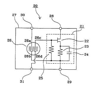
FIG. 1 shows an embodiment of the oscillator module of
the present invention.
In FIG. 1, an oscillator module 20 comprises a circuit
portion for oscillation 21 and a two-port surface acoustic
wave resonator 26, these being hermetically sealed in a
package 27. First external terminals 28 and 29 and second
CA 02274335 1999-06-11
__
external terminals 30 and 31 are provided at the package 27.
The circuit portion for oscillation 21 comprises a FET
22, resistors 23 and 25, and a capacitor 24. The drain of
the FET 22 is connected to the first external terminal 28.
The source of the FET 22 is connected via the resistor 23 to
the first external terminal 29, and the capacitor 24 is
connected in parallel with the resistor 23. Furthermore,
the resistor 25 is connected between the gate of the FET 22
and the first external terminal 29. As a result, circuit
portion for oscillation 21 comprises an amplifier having the
gate of the FET 22 as its input terminal and the drain as
its output terminal.
Furthermore, the two-port surface acoustic wave
resonator 26 has two terminals 26a and 26b, used as ports
for input, and two terminals 26c and 26d, used as ports for
output. The terminal 26a of the two-port surface acoustic
wave resonator 26 is connected to one of the second external
terminals, 30, and the terminal 26d is connected to the
other second external terminal 31.
The terminal 26c of the two-port surface acoustic wave
resonator 26 is connected within the package 27 to the gate
of the FET 22, that is, to the input terminal of the circuit
portion for oscillation 21. Furthermore, the terminal 26b
of the two-port surface acoustic wave resonator 26 is
connected to the first external terminal 29.
CA 02274335 1999-06-11
__ g _
FIG. 2 shows a perspective view of the oscillator
module 20 shown in FIG. 1. In FIG. 2, the oscillator module
20 comprises (i) a circuit portion for oscillation 21,
implemented as a bare-chip integrated circuit, and (ii) a
bare-chip two-port surface acoustic wave resonator 26, these
being mounted in a concave component mount portion provided
at substantially the center of a substrate-like package 27.
First external terminals 28 and 29 and second external
terminals 30 and 31 are provided on side faces of the
package 27. The circuit portion for oscillation 21 and the
two-port surface acoustic wave resonator 26 are connected by
wires 33 and internal electrodes 32, inside the package 27.
The internal electrodes 32 are connected to the first
external terminals 28 and 29 and the second external
terminals 30 and 31. A cover 34 is attached over the
package 27 and completely covers the circuit portion for
oscillation 21, the two-port surface acoustic wave resonator
26, the internal electrodes 32 and the wires 33.
FIG. 3 shows an embodiment of an oscillator utilizing
the oscillator module 20. In the oscillator module 40 shown
in FIG. 3, the first external terminal 29 and the second
external terminal 31 of the oscillator module 20 are
grounded. Further, the first external terminal 28 and the
second external terminal 30 are connected by an external
wire 41. The first external terminal 28 is connected via an
CA 02274335 1999-06-11
-- 9 -
inductor 42, to a power supply terminal 43. The first
external terminal 28 is connected, via a capacitor 44, to an
output terminal 45. As a result, the two-port surface
acoustic wave resonator 26 has the terminal 26a as its input
terminal, and the terminal 26c as its output terminal.
In this way, the oscillator module 20 functions as an
oscillator by connecting some of the external terminals
using external wire. Therefore, the number of external
terminals provided to the package can be reduced versus when
the resonator and the circuit portion for oscillation are
provided completely separately in the package. The
oscillator module is, thus, smaller and of lower cost.
Furthermore, since there are fewer external wires, the costs
of constructing the oscillator can be reduced, and variation
in the characteristics (due to the external wires) is
likewise reduced.
FIG. 4 shows a measuring system for measuring resonant
frequency and insertion loss of the two-port surface
acoustic wave resonator 26 in the oscillator module 20 shown
in FIG. 1. In FIG. 4, the second external terminals 30 and
31 are connected to a measuring device 50, such as a network
analyzer. The first external terminals 28 and 29 are
grounded.
In the measuring system of FIG. 4, the measuring device
50 is able to measure the resonant frequency and the
CA 02274335 1999-06-11
-- 10 -
insertion loss between terminal 26a and terminal 26d of the
two-port surface acoustic wave resonator 26. In the
oscillator 40 of FIG. 3, the two-port surface acoustic wave
resonator 26 used terminal 26a as its input terminal and
terminal 26c as its output terminal, and therefore it was
necessary to measure the characteristics between terminal
26a and terminal 26c. However, the characteristics between
terminal 26a and terminal 26d are merely 180 degrees out of
phase with the characteristics between terminal 26a and
terminal 26c, and consequently there is absolutely no
difficulty in measuring the resonant frequency and the
insertion loss.
Furthermore, although terminal 26b is directly
grounded, terminal 26c is grounded via the circuit portion
for oscillation 21, and therefore it cannot be said that the
actual characteristics of the two-port surface acoustic wave
resonator 26 are being measured. However, even when a
slight impedance is inserted between terminal 26c and
ground, the insertion loss and resonant frequency can be
measured in almost the same manner as when terminal 26c is
directly grounded, without difficulty.
Furthermore, FIG. 5 shows a measuring system for
measuring the oscillation margin of the oscillator module 20
shown in FIG. 1. In FIG. 5, the first external terminal 28
and the second external terminal 30 are connected to a
CA 02274335 1999-06-11
-- 11 -
measuring device 51, such as a network analyzer.
Furthermore, the first external terminal 29 and the second
external terminal 31 are grounded. Direct current or the
like is supplied to the circuit portion for oscillation 21
through the measuring device 51.
In the measuring system of FIG. 5, the measuring device
51 is inserted at a position on the external wire 41, which
connects the first external terminal 28 and the second
external terminal 30 of the oscillator module 20 in the
oscillator 40 of FIG. 3. That is, the measuring device 51
is inserted in part of the oscillation loop. In this state,
the oscillation margin of the oscillator module 20 can be
measured by measuring the transmission characteristics
(amplitude and phase) when a signal is input from the second
external terminal 30 and a signal is output from the first
external terminal 28.
The oscillator 40 can be formed in compliance with the
result of the measurements taken using the measuring systems
of FIG. 4 and FIG. 5, by adjusting the length of the
external wire 41, and inserting a capacitor and inductor for
adjusting midway along the external wire 41, so that the
oscillator 40 has a large oscillation margin. As a result,
it is possible to accommodate changes in characteristics
when the oscillator module is hermetically sealed in a
package, improving the yield of the oscillator 40 and
CA 02274335 1999-06-11
-- 12 -
reducing costs.
FIG. 6 shows an embodiment of a communications device
of the present invention, being a partially cut away view
of a key (single-unit) transmitter for a keyless entry
system. The key uses the oscillator 40 shown in FIG. 3. In
FIG. 6, the transmitter 60 comprises a key portion 61 and a
grip portion 62, which are joined together. The grip
portion 62 contains an antenna 63, an oscillator 40, a
modulator 64, a code generator 65 and a power supply circuit
66. Furthermore, a switch 67 is provided at the grip
portion 62. The code generator 65 is connected, via the
modulator 64, to the antenna 63, and the oscillator 40 is
connected to the modulator 64. The power supply circuit 66
is connected to the oscillator 40, the modulator 64 and the
code generator 65.
When the switch 67 is pressed, the code generator 65
generates a specific digital code corresponding to the
particular key. In compliance with the digital code
generated by the code generator 65, the modulator 64
modulates an RF signal, input from the oscillator 40. The
antenna 63 radiates the modulated RF signal.
Thus, the transmitter for keyless entry system, which
uses a communications device having an oscillator module of
the present invention, enjoys reduced oscillator variation.
Consequently, the yield of the transmitter is improved, and
CA 02274335 1999-06-11
-- 13 -
the elimination of adjustment costs enables the device to be
made at a low price.
The oscillator module of the present invention
comprises a circuit portion for oscillation, a two-port
surface acoustic wave resonator, whose two ports each
comprise two terminals, a package in which the circuit
portion for oscillation and the two-port surface acoustic
wave resonator are sealed, a first external terminal,
provided at the package and connected to the circuit portion
for oscillation, and a second external terminal connected to
one of the terminals of the two-port surface acoustic wave
resonator, the remaining terminals of the two-port surface
acoustic wave resonator being connected to the circuit
portion for oscillation inside the package.
Therefore, the number of external terminals provided at
the package can be reduced versus when the resonator and the
circuit portion for oscillation are provided completely
separately inside the package, enabling the oscillator
module to be made small-scale and at lower cost.
Furthermore, since there are fewer external wires, the costs
of manufacturing the oscillator can be reduced. Variation
in the characteristics of the oscillator (due to the
external wires) is likewise reduced. Furthermore, it is
possible to measure the insertion loss and resonant
frequency of the two-port surface acoustic wave resonator,
CA 02274335 1999-06-11
-- 14 -
and the oscillation margin of the oscillator module.
Therefore, by adjusting the external wires accordingly,
changes in the characteristics of the circuit portion for
oscillation and the two-port surface acoustic wave
resonator, which occur when they are hermetically sealed
inside the package, can be accommodated, thereby improving
the yield of the oscillator and reducing costs.
Furthermore, by using the oscillator module of the
present invention in a communications device, the reduced
oscillator variation improves the yield of the
communications device, and the elimination of adjustment
costs enables it to be made at a low price.
Although the present invention has been described in
relation to particular embodiments thereof, many other
variations and modifications and other uses will become
apparent to those skilled in the art. It is preferred,
therefore, that the present invention be limited not by the
specific disclosure herein, but only by the appended claims.