Note: Descriptions are shown in the official language in which they were submitted.
CA 02274391 1999-06-11
1
IMAGE PROCESSING APPARATUS
BACKGROUND OF THE INVENTION
1. Field of the Invention
The present invention relates to a graphic
image processing apparatus, more specifically relates to
the technical field of arrangement and interconnection of
a built-in memory especially in the case where a DRAM or
other memory and a logic circuit are provided together.
2. Description of the Related Art
Computer graphics are often used in a variety
of CAD (computer aided design) systems and amusement
machines. Especially, along with the recent advances in
image processing techniques, systems using three-
dimensional computer graphics are becoming rapidly
widespread.
In three-dimensional computer graphics, the
color value of each pixel is calculated at the time of
deciding the color of each corresponding pixel. Then,
rendering is performed for writing the calculated value
to an address of a display buffer (frame buffer)
corresponding to the pixel.
One of the rendering methods is polygon
rendering. In this method, a three-dimensional model is
expressed as a composite of triangular unit graphics
CA 02274391 1999-06-11
2
(polygons). By drawing using the polygons as units, the
colors of the pixels of the display screen are decided.
In polygon rendering, coordinates (x, y, z),
color data (R, G, B), homogeneous coordinates (s, t) of
texture data indicating a composite image pattern, and a
value of the homogeneous term g for the respective
vertexes of the triangle in a physical coordinate system
are input and processing is performed for interpolating
these values inside the triangle.
Here, coordinates in a UV coordinate system
of an actual texture buffer, namely, texture coordinate
data (u, v), are comprised of the homogeneous coordinates
(s, t) divided by the homogeneous term g to give "s/q"
and "t/q" which in turn are multiplied by texture sizes
USIZE and VSIZE, respectively.
Figure 11 is a view of the system
configuration of the basic concept of a three-dimensional
computer graphic system.
In the three-dimensional computer graphic
system, data for drawing a graphic image is given from a
main memory 2 of a main processor 1 or an I/O interface
circuit 3 for receiving external graphic data to a
rendering circuit 5 having a rendering processor 5a and a
frame buffer 5b via a main bus 4.
The rendering processor 5a is connected to a
CA 02274391 1999-06-11
3
frame buffer 5b intended to hold data for display and a
texture memory 6 for holding texture data to be applied
on the surface of a graphic element to be drawn (for
example, a triangle).
The rendering processor 5a is used to perform
the processing for drawing a graphic element with a
texture applied to its surface in the frame buffer 5b for
every graphic element.
The frame buffer 5b and the texture memory 6
are generally composed by a dynamic random access memory
(DRAM).
In the system shown in Fig. 11, the frame
buffer 5b and the texture memory 6 are configured as
physically separate memory systems.
Recently, it has become possible to provide a
DRAM and a logic circuit.together. Looking at graphic
drawing image processing apparatuses, as shown in Fig.
12, there are ones attempting to build a DRAM or other
large capacity memory 7a on the, same semiconductor chip 7
as a drawing use logic circuit 7b while keeping the
previous structure of use of an external memory as it is.
In this case, a DRAM core having an
equivalent control mechanism as a general-purpose DRAM is
simply arranged next to the prior graphic drawing image
processing logic circuit and the two are interconnected
CA 02274391 1999-06-11
4
by a single path.
There are only the above types in the case of
graphic drawing image processing apparatuses.
Below, although the technical field is
different from that of a graphic drawing image processing
apparatus, the trends in the field of microprocessors
will be described.
In the past, it has been proposed to provide
a microprocessor and a memory on a single chip. Proposals
have also been made regarding the arrangement of the
memory on the chip.
For example, in a PPRAM
(ISSCC97/SESSION14/Parallel Processing RAM), as shown in
Fig. 13, DRAMs 8a-1 to 8a-4 serving as main memories and
microprocessors (P) 8b-1 to 8b-4 are built in on the same
semiconductor chip 8.
Note that, in Fig. 13, reference numerals 8c-
1 to 8c-4 indicate memory controllers (Mem CTL) of the
DRAMs 8a-1 to 8a-4, and 8d-1 tQ 8d-4 indicate caches.
In this semiconductor chip 8, the DRAMs 8a-1
to 8a-4 serving as the main memories are arranged in only
one direction with respect to the microprocessors 8b-1 to
8b-4.
Also, Fig. 13 shows a configuration wherein a
plurality of microprocessors 8b-1 to 8b-4 access single
CA 02274391 1999-06-11
DRAMs via the caches 8d-1 to 8d-4.
Turning to the problems to be solved by the
invention, in the above conventional so-called built-in
DRAM system, however, when a frame buffer memory and a
5 texture memory are separated into different memory
systems, there is a disadvantage that the frame buffer
emptied due to a change of the display resolution cannot
be used for the texture. Alternatively, when the frame
memory and the texture memory are physically combined,
the overhead of the page exchange of the DRAM etc.
becomes large at the time of simultaneous success of the
frame memory and the texture memory, so there is a
disadvantage that the performance has to be sacrificed.
Also, with a method of interconnection
wherein a DRAM core having a control mechanism equivalent
to a general-purpose DRAM is arranged next to a graphic
image processing logic circuit and the two are connected
by a single path, the bandwidth for accessing is not
improved at all in spite of the trouble of building in
the DRAM and becomes a bottleneck in system performance.
Furthermore, a built-in main memory type
microprocessor has the following disadvantages:
Namely, the semiconductor chip 8 has four
units of the same functional configuration aligned with
each other and transfers data through the memory
CA 02274391 1999-06-11
6
controllers. The bandwidths of the transfer are
determined by the path widths of the memory controllers
and the operating speeds. The fastest path is one cutting
straight across the chip. The operating speed is
determined by the longest path. Therefore, improvement of
the operating speed becomes difficult. Long paths
naturally occupy a greater area in the layout.
The trend has been for the speed of
microprocessors to double every 18 months and for the
memory capacity to also double about every 18 months.
In spite of this situation, the access time
increases about 7% per year. How to make the access time
faster is now becoming the key to improving the system
performance.
In the above conventional method, the larger
the chip, the longer the critical path and therefore the
more the operating speed ends up being hampered.
Accordingly, the access time between DRAMs is
left unimproved, so the merits.of building in DRAMs do
not appear that much.
SUMMARY OF THE INVENTION
An object of the present invention is to provide an
image processing apparatus capable of effectively
utilizing a storage circuit provided together with a
logic circuit and enabling an increase of the operating
__ ....__..w......
CA 02274391 1999-06-11
7
speed and reduction of the power consumption without
causing a deterioration of performance.
According to a first aspect of the present
invention, there is provided n image processing apparatus
comprising a storage circuit divided into a plurality of
storage modules, each storage module storing image data
of different pixels and a logic circuit for performing
predetermined processing on the image data based on the
stored data of the storage circuit, the storage circuit
and the logic circuit being both accommodated on one
semiconductor chip, and the plurality of divided storage
modules arranged at peripheral portions of the logic
circuit.
According to a second aspect of the invention,
there is provided an image processing apparatus for
performing rendering by receiving polygon rendering data
including three-dimensional coordinates (x, y, z), R
(red), G (green), and B (blue) data, homogeneous
coordinates (s, t) of texture,,and a homogeneous term q
for vertexes of a unit graphic; comprising a storage
circuit divided into a plurality of storage modules, each
storage module storing display data of different pixels
and texture data required by at least one graphic element
and a logic circuit comprising at least an interpolation
data generating circuit for performing interpolation on
CA 02274391 1999-06-11
8
the polygon rendering data of the vertexes of the unit
graphic to generate interpolation data of pixels
positioned inside the unit graphic and a texture
processing circuit for dividing the homogeneous
coordinates (s, t) of texture included in the
interpolation data by the homogeneous term q to generate
"s/q" and "t/q", using texture addresses in accordance
with the "s/q" and "t/q" to read texture data from the
storage circuit, and performing processing for applying
the texture data to the surface of the graphic elements
of the display data, and the storage circuit and the
logic circuit being both accommodated on one
semiconductor chip, and having the plurality of divided
storage modules arranged at peripheral portions of the
logic circuit.
Preferably, the logic circuit is divided into a
plurality of pixel processing blocks corresponding to the
storage modules and each corresponding pixel processing
block is closely arranged to each storage module.
Preferably, further provision is made of a
secondary memory capable of storing stored data of a
storage module and the secondary memory is closely
arranged to the storage module.
Preferably, a pixel processing block performs at
least one stage of pipeline processing therein.
CA 02274391 1999-06-11
9
Preferably, the storage modules are arranged at
peripheral portions of the logic circuit so as to
surround the logic circuit and wherein input/output
terminals are arranged at the inside edges facing the
logic circuit.
Preferably, the plurality of pixel processing
blocks, even if for modules having the same function, are
changed in the positions of their terminals for taking
out paths so as to enable paths to be optimally laid to
pixel processing blocks using paths from the storage
modules.
Preferably, there is further provided a control
block equivalently connected to all of the storage
modules for controlling the operations of the above
plurality of storage modules and that control block is
arranged close to a center point surrounded by the
storage modules.
Preferably, the storage circuit is accessed based
on a row address and a column ,address; the logic circuit
is divided into a plurality of pixel processing blocks
corresponding to the storage modules, a corresponding
pixel processing block being closely arranged at each
storage module; there is a secondary memory capable of
storing the stored data of a storage module, which
secondary memory is arranged close to a storage module;
CA 02274391 1999-06-11
the storage module is arranged so that its longitudinal
direction is the column direction of a core; and the
pixel processing block and the secondary memory are
arranged close to each other on the same side of the long
5 side of the storage module.
Explained from another angle, in the present
invention, the storage circuit is composed of a plurality
of independent modules. Due to this, the ratio of valid
data held in a bit line in one access increases comparing
10 with the case where accesses have to be made
simultaneously.
The plurality of divided storage modules are
arranged at the peripheral portions of the logic circuit
portion for carrying out graphic drawing processing etc.
As a result, the distances from the respective
storage modules to the logic circuit portion become
uniform and the length of the longest path
interconnection is shortened compared with the case where
the modules are all arranged in one direction. Therefore,
the operating speed as a whole is improved.
Also, a function block for controlling pixel
processing in the graphic drawing is arranged close to
each of the storage modules of the storage circuit.
Therefore, read/modify/write processing, which is
carried out for an extremely large number of times in
CA 02274391 1999-06-11
11
graphic processing, can be performed in a very short
interconnection region. Therefore, the operating speed is
strikingly improved.
At each storage module, a secondary memory is
closely arranged to the module.
Due to this, even when data is transferred from a
storage circuit to a secondary memory by a path having a
very wide width, there is little effect of so-called
cross talk. Also, since the interconnection length is
naturally short, the operating speed is improved.
Further, the area occupied by the interconnections
becomes small as well.
By having a function block for controlling the
pixel processing in the graphic drawing perform at least
one stage of pipeline processing therein, even if the
distance to a block carrying out other graphic processing
arranged at the center becomes long on an average, it is
possible to eliminate the effect on the through-put for
processing data and therefore the processing speed is
improved.
Further, the input/output terminals at the modules
arranged at the peripheral portions of the logic circuit
portion for carrying out the graphic drawing processing
etc. so as to surround the same are arranged at the inner
sides facing the logic circuit portion.
CA 02274391 1999-06-11
12
Due to this, the interconnection region is orderly
and the average interconnection length becomes shorter.
Also, a plurality of function blocks for
controlling the pixel processing, even if they are for
modules having the same function, are changed in the
positions of their terminals for taking out paths so as
to enable paths to be optimally laid to function blocks
using paths from the modules.
Due to this, even if the same in function, the
terminals of the blocks can be arranged at the optimal
positions for the locations of arrangement of the blocks,
so the average interconnection length becomes shorter.
Also, the block having the largest number of
interconnections among blocks equally connected to all of
the storage modules is arranged close to the center point
surrounded by the storage circuits.
As a result, the area occupied by the
interconnections becomes smaller and the longest
interconnection length becomes,shorter. Therefore, the
operating speed can be simultaneously improved as well.
When, for every module, a function block for
controlling the pixel processing in the graphic drawing
and a secondary memory are closely arranged to the
storage module, the storage modules are arranged so that
their longitudinal directions becomes the same as the
CA 02274391 1999-06-11
13
column direction of a core of the storage circuit (for
example, DRAM).
As a result, comparing with arrangement in the row
direction, by just specifying the row address, the one
row's worth of data corresponding to that row address can
be loaded into the secondary memory at one time, that Is,
the number of bits is dramatically increased.
The pixel processing block and the secondary memory
are closely arranged to each other on the same side of a
longitudinal side of the storage module.
As a result, data to the pixel processing block and
the secondary memory can use the same sense amplifier.
Therefore, the increase of the area of the core of the
storage circuit can be kept to a minimum and two ports
become possible.
BRIEF DESCRIPTION OF THE DRAWINGS
These and other objects and features of the present
invention will become clearer from the following
description of the preferred embodiments given with
reference to the attached drawings, in which:
Fig. 1 is a block diagram of the configuration of a
three-dimensional computer graphic system according to
the present invention;
Fig. 2 is a view for explaining the function of a
DDA set-up cirouit according to the present invention;
CA 02274391 1999-06-11
14
Fig. 3 is a view for explaining the function of a
triangle DDA circuit according to the present invention;
Fig. 4 is a view for explaining sorting of vertexes
of the triangle DDA circuit according to the present
invention;
Fig. 5 is a view for explaining inclination
calculation in the horizontal direction of the triangle
DDA circuit according to the present invention;
Fig. 6 is a view for explaining an interpolation
routine of vertex data of the triangle DDA circuit
according to the present invention;
Fig. 7 is a flow chart for explaining the
interpolation routine of vertex data of the triangle DDA
circuit according to the present invention;
Fig. 8 is a view for explaining a method of storing
data according to the present invention;
Fig. 9 is a view for explaining a preferable
configuration, arrangement, and interconnection method of
a logic circuit of the rendering circuit, DRAM, and
secondary memory provided together on one semiconductor
chip according to the present invention;
Fig. 10 is a view for explaining an example of the
configuration of a DRAM module according to the present
invention;
Fig. 11 is a view of the system configuration of
CA 02274391 1999-06-11
the basic concept of a three-dimensional computer graphic
system;
Fig. 12 is a view for explaining the general
arrangement and configuration in a case of providing a
5 DRAM having a large capacity and a logic circuit together
on a semiconductor chip; and
Fig. 13 is a view for explaining an example of the
configuration for providing a microprocessor and a memory
on one chip.
10 DESCRIPTION OF THE PREFERRED EMBODIMENTS
Below, in the present embodiment, an explanation
will be made of a three-dimensional computer graphic
system which is applied to a personal computer and the
like and is able to display a desired three-dimensional
15 image of any three-dimensional object model on a display
such as a cathode ray tube (CRT) at a high speed.
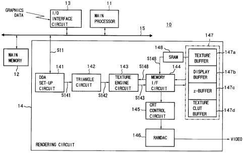
Figure 1 is a view of the system configuration of a
three-dimensional computer graphic system 10 serving as
an image processing apparatus according to the present
invention.
In the three-dimensional computer graphic system
10, a three-dimensional model is expressed by a composite
of triangular unit graphics (polygons). By drawing the
polygons, this system can decide the color of each pixel
on the display screen and perform polygon rendering for
CA 02274391 1999-06-11
16
display on the screen.
In the three-dimensional computer graphic system
10, a three-dimensional object is expressed by using a z-
coordinate for indicating the depth in addition to the
(x, y) coordinates for indicating positions on a two-
dimensional plane. Any one point of the three dimensional
space can be expressed by the three coordinates (x, y,
z).
As shown in Fig. 1, the three-dimensional computer
graphic system 10 is comprised of a main memory 12, an
I/O interface circuit 13, and a rendering circuit 14
connected via a main bus 15.
Below, the operations of the respective components
will be explained.
The main processor 11, for example, in accordance
with the state of progress in a game, reads the necessary
graphic data from the main memory 12 and performs
clipping, lighting, geometrical processing, etc. on the
graphic data to generate polygon rendering data. The main
processor 11 outputs the polygon rendering data Sil to
the rendering circuit 14 via the main bus 15.
The I/O interface 13 receives as input motion
control information or the polygon rendering data from
the outside in accordance with need and outputs the same
to the rendering circuit 14 via the main bus 15.
CA 02274391 1999-06-11
17
Here, the polygon rendering data includes data of
each of the three vertexes (x, y, z, R, G, B, s, t, q) of
the polygon.
Here, the (x, y, z) data indicates the three-
dimensional coordinates of a vertex of the polygon, and
(R, G, B) data indicates the luminance values of red,
green, and blue at the three-dimensional coordinates,
respectively.
Among the (s, t, q) data, the (s, t) indicates
homogeneous coordinates of a corresponding texture and
the g indicates the homogenous term. Here, the texture
size USIZE and VSIZE are respectively multiplied with the
"s/q" and "t/q" to obtain coordinate data (u, v) of the
texture. The texture coordinate data (u, v) is used for
accessing the texture data stored in the texture buffer
147a.
Namely, the polygon rendering data indicates
physical coordinate values of the vertexes of a triangle
and values of colors of the vertexes and texture data.
The rendering circuit 14 will be explained in
detail below.
As shown in Fig. 1, the rendering circuit 14
comprises a digital differential analyzer (DDA) set-up
circuit 141, a triangle DDA circuit 142, a texture engine
circuit 143, a memory interface (I/F) circuit 144, a CRT
CA 02274391 1999-06-11
18
control circuit 145, a random access memory digital to
analog converter (RAMDAC) circuit 146, a DRAM 147, and a
static random access memory (SRAM) 148.
The rendering circuit 14 of the present embodiment
is provided with a logic circuit and a DRAM 147 for
storing at least display data and texture data together
in one semiconductor chip.
The DRAM 147 functions as a texture buffer 147a, a
display buffer 147b, z-buffer 147c, and a texture color
look-up table (CLUT) buffer 147d.
The DRAM 147 is, as will be explained below,
divided into a plurality of modules (four in this
embodiment) having the same function.
Indexes in index colors and values of the color
look-up table therefor are stored in the texture CLUT
buffer 147d in the DRAM 147 for storing more texture
data.
The indexes and values of the color look-up table
are used for the texture processing. Namely, a texture
element is normally expressed by the total 24 bits of the
8 bits of each of R, G, and B. However, the data amount
swells up in this way, so one color is selected from
among, for example, 256 colors selected in advance, to
use for the texture processing. As a result, with 256
colors, the texture elements can be expressed by 8 bits.
CA 02274391 1999-06-11
19
A conversion table from the indexes to an actual color is
necessary, however, the higher the resolution of the
texture, the more compact the texture data can become.
Due to this, compression of the texture data
becomes possible and the built-in DRAM can be used
efficiently.
Further, depth information of the object to be
drawn is stored in the DRAM 147 in order to perform
hidden plane processing simultaneously and in parallel
with the drawing.
Note that as a method of storing the display data,
the depth data, and the texture data, the display data is
stored continuously from the top of the memory block,
then the depth data is stored, and then the texture data
is stored in continuous address spaces for each type of
texture in the remaining vacant region. As a result, the
texture data can be efficiently stored.
DDA Set-up Circuit 141
The DDA set-up circuit 141 performs linear
interpolation on the values of the vertexes of the
triangle on the physical coordinates in a triangle DDA
circuit 142 in its latter part. The DDA set-up circuit
141, prior to obtaining information of the color and
depth of the respective pixels inside the triangle,
performs a set-up operation for obtaining the sides of
CA 02274391 1999-06-11
the triangle and the difference in a horizontal direction
for the data (z, R, G, B, s, t, q) indicated by the
polygon rendering data S11.
Specifically, this set-up operation uses values of
5 the starting point and the ending point and the distance
between the two points to calculate the variation of the
value to find movement for a unit length.
The DDA set-up circuit 141 outputs the calculated
variation data S141 to the triangle DDA circuit 142.
10 The function of the DDA set-up circuit 141 will be
further explained with reference to Fig. 2.
As explained above, the main processing of the DDA
set-up circuit 141 is to obtain the change inside a
triangle composed of three vertexes given various
15 information (color and texture coordinates) at vertexes
reduced to physical coordinates through the former
geometric processing so as to calculate basic data for
the later linear interpolation.
Note that the data of each vertex of the triangle
20 is, for example, configured by 16 bits of x- and y-
coordinates, 24 bits of the z-coordinate, 12 bits (=8+4)
of the color values for the RGB, and 32 bits of floating
decimal values (IEEE format) of the s, t, q texture
coordinates.
While the drawing of a triangle is reduced to the
CA 02274391 1999-06-11
21
drawing of a horizontal line, this makes it necessary to
obtain the starting values at the starting point of the
drawing of the horizontal line.
In drawing the horizontal line, the direction of
drawing is made constant in one triangle. For example,
when drawing from the left to the right, the X with
respect to a displacement in the Y-direction of a side on
the left and the above various changes are calculated
first, then these are used to find the X-coordinate of
the left-most point when moving from a vertex to the next
horizontal line and values of the above various
information (points on a side change in both the X- and
Y-directions, so calculation is impossible only from the
inclination of the Y-direction).
Only the position of the end point is required for
the side on the right, so only the change of x with
respect to the displacement in the Y-direction need be
investigated.
Regarding the drawing of.a horizontal line, since
the inclination in the horizontal direction is uniform in
the same triangle, the inclinations of the above various
information are calculated.
The given triangle is sorted in the Y-direction and
the upper-most point is set to be A. Next, the remaining
two vertexes are compared in terms of the positions in
CA 02274391 1999-06-11
22
the X-direction and the point on the right is set to be
B. By doing this, the processing can be divided into only
two or so steps.
Triangle DDA Circuit 142
The triangle DDA circuit 142 uses the variation
data S141 input from the DDA set-up circuit 141 to
calculate the linearly interpolated (z, R, G, B, s, t, q)
data for each pixel inside the triangle.
The triangle DDA circuit 142 outputs the data (x,
y) for each pixel and the (z, R, G, B, s, t, q) data at
the (x, y) coordinates to the texture engine circuit 143
as DDA data (interpolation data) S142.
For example, the triangle DDA circuit 142 outputs
the DDA data S142 of 8 (=2x4) pixels positioned inside a
block being processed in parallel to the texture engine
circuit 143.
A further explanation will be made of the function
of the triangle DDA circuit 142 with reference to Fig. 3.
As explained above, inclination information of the
above various information of the sides and horizontal
direction of a triangle is prepared by the DDA set-up
circuit 141. The basic processing of the triangle DDA
circuit 142 receiving this information consists of the
calculation of the initial values of the horizontal line
by interpolation of the various information on the sides
CA 02274391 1999-06-11
23
of the triangle and the interpolation of the various
information on the horizontal line.
Here, what must be noted most is that the
calculation of results of the interpolation requires
calculation of the values at the center of a pixel.
The reason is that if the value calculated is off
from the center of the pixel, while there is not much to
worry about in the case of a still picture, the
flickering of the image will stand out in a motion
picture.
The various information at the left-most side of a
first horizontal line (line naturally connecting the
centers of pixels) can be obtained by multiplying the
inclination on the side with the distance from the vertex
to the first line.
The various information at the starting point of
the next line can be calculated by adding the inclination
of the side.
The value at the first pixel of the horizontal line
can be calculated by adding the value obtained by
multiplying the distance to the first pixel with the
inclination in the horizontal direction to the value at
the starting point of the line. The value at the next
pixel of the horizontal line can be calculated by adding
to the first pixel value the inclination in the
CA 02274391 1999-06-11
24
horizontal direction successively.
Next, sorting of vertexes will be explained with
reference to Fig. 4.
By sorting the vertexes in advance, tr,.: branching
of the successive processing can be reduced to a minimum
and contradictions can be made harder to occur inside one
triangle as much as possible even in interpolation.
As the method of sorting, first, all of the
vertexes supplied are sorted in the Y-direction and the
upper-most point and the lower-most point are defined as
the point A and point C, respectively. The remaining
point is defined as the point B.
By doing so, in the processing, the side extending
the longest in the Y-direction becomes a side AC. First,
the side AC and the side AB are used for the
interpolation of the region between the two sides, then
interpolation is performed for the region between the
side BC and the side AC, that is, leaving the side AC as
it is and changing from the side AB. Also, it will be
understood that it is sufficient to perform processing
with respect to the side AC and the side BC for
correction on the pixel coordinate lattice in the Y-
direction.
Since branching of the processing after sorting
becomes unnecessary in this way, the processing can be
CA 02274391 1999-06-11
performed by simply supplying the data, bugs can be
prevented from occurring, and the configuration becomes
simple.
Also, since the direction of the interpolation in
5 one triangle can be made constant by setting a starting
point on the side BC, the direction of interpolation
(span) in the horizontal direction becomes constant and
any computation errors which occur are accumulated from
the side BC to other sides. Since the direction of the
10 accumulation becomes constant, errors between adjacent
sides become less conspicuous.
Next, the calculation of the inclination in the
horizontal direction will be explained with reference to
Fig. 5.
15 The inclination (variable worth) of the variables
(x, y, z, R, G, B, s, t, q) inside a triangle with
respect to (x, y) becomes constant due to the linear
interpolation.
Accordingly, the inclination in the horizontal
20 direction, that is, the inclination on each of the
horizontal lines (span), becomes constant for all spans,
so the inclination is obtained prior to the processing of
the spans.
As a result of sorting the given vertexes of the
25 triangle in the Y-direction, the side AC is defined again
CA 02274391 1999-06-11
26
to be the longest extending side, so there is always a
point of intersection of a line extending from the vertex
B in the horizontal direction and the side AC. The point
is defined as D.
After this, by just obtaining the change between
the point B and D, the inclination in the horizontal
direction, that is, in the x-direction, can be obtained.
Specifically, the x- and z-coordinates at the point
D become as shown in the equations below.
xd= { ( Yd - Ya ) / ( Yc - ya ) }' ( Xc - Xa )
zd={(Yd-Ya)/(Yo-Ya)}=(za-za)
When obtaining the inclination of the variable z in
the x-direction based on this, the following is obtained:
AZ/OX =(Zd-Zb)/(Xd-Xb)
=[{(Yd-Ya)/(Yc-Ya)}'(Zc-Za)-Zbl/
I{(Yd-Ya)/(Yc-Ya)}=(xc-xa)-Xbl
={zb(Yc-Ya) -( zc-za) (Yc-Ya)}/
(xb(yc-Ya) - ( zc - za) (Yc-Ya)}
Next, an example of the routine for interpolation
of vertex data will be explained with reference to Figs.
6A, 6B, and 7.
After the processing for sorting the vertexes,
calculating the inclination in the horizontal direction,
and calculating the inclination on each of the sides,
interpolation is carried out using the results.
CA 02274391 1999-06-11
27
Depending the position of the point B, the
processing at a span splits in two directions. This is
because it is desired to perform the processing by always
using the side extending the longest in the Y-direction
as a starting point so as to try to prevent trouble as
much as possible by making the direction of accumulation
of errors between respective spans in interpolation
inside one triangle constant.
When the point B is at the same height as the point
A, the first half of the processing is skipped.
Therefore, the processing can be streamlined by just
providing a skippable mechanism rather than branching.
When trying to improve the processing capability by
simultaneously processing a plurality of spans, it is
desired to obtain the inclination in the Y-direction,
however it is necessary to carry out the processing again
from the sorting of the vertexes. However, the processing
before the interpolation processing is enough, so the
processing system as a whole becomes simpler.
Specifically, when the point B is not the same
height as the point A, Y-direction correction of AC and
AB (calculation of values on a pixel lattice) is
performed (ST1 and ST2) and the interpolation on the side
AC and the interpolation on the side AB are performed
( ST3 ) .
CA 02274391 1999-06-11
28
Then, the correction in the AC horizontal direction
and the interpolation on the horizontal line (span) from
the side AC in the side AB direction (ST4) are carried
out.
The above processing of steps ST3 and ST4 are
performed until the end of the side AB (ST5).
When the processing of steps ST2 to ST4 until the
end of the side AB is completed or when it is judged at
step ST1 that the point B is the same height as the point
A, the Y-direction correction of BC (calculation of
values on the pixel lattice) is carried out (ST6) and the
interpolation on the side AC and the interpolation on the
side BC are carried out (ST7).
Then, the correction in the AC horizontal direction
and the interpolation on the horizontal line (span) are
carried out (ST8).
The processing of the above steps ST7 and ST8 is
carried out until the end of the side BC (ST9).
Texture Engine Circuit 143
The texture engine circuit 143 performs the
calculation of "s/q" and "t/q", calculation of the
texture coordinate data (u, v), and reading of the data
(R, G, B) from the texture buffer 147a successively in a
pipeline format.
Note that the texture engine circuit 143 performs
CA 02274391 1999-06-11
29
the processing on the 8 pixels positioned inside a
predetermined block simultaneously in parallel.
The texture engine circuit 143 performs the
operation for dividing the data s by the data g and the
operation for dividing the data t by the data g on the
(s, t, q) data indicated by the DDA data S142.
The texture engine circuit 143 is provided with for
example eight not illustrated division circuits and
performs the division "s/q" and "t/q" simultaneously on
the 8 pixels.
Also, the texture engine 143 respectively
multiplies the texture sizes USIZE and VSIZE with the
division results "s/q" and "t/q" to generate the texture
coordinate data (u, v).
The texture engine circuit 143 outputs a read
request including the generated texture coordinate data
(u, v) to the SRAM 148 or DRAM 147 via the memory I/F
circuit 144. As the result the texture engine circuit 143
obtains the (R, G, B) data S148 stored at the texture
address corresponding to the data (s, t) by reading the
texture data stored in the SRAM 148 or in the texture
buffer 147a via the memory I/F circuit 144.
Here, the texture data stored in the texture buffer
147a is stored in the SRAM 148.
The texture engine circuit 143 generates pixel data
CA 02274391 1999-06-11
S143 by multiplying the (R, G, B) data in the read (R, G,
B) data S148 and the (R, G, B) data included in the DDA
data S142 from the triangle DDA circuit 142 in the former
stage.
5 The texture engine circuit 143 outputs.the pixel
data S143 to the memory I/F circuit 144.
Note that in the texture buffer 147a, MIPMAP
(texture for a plurality of resolutions) or other texture
data corresponding to a plurality of reducing rates is
10 stored. Here, texture data of which reducing rate to use
is determined for the above triangular unit using a
predetermined algorithm.
In the case of a full color mode, the texture
engine circuit 143 directly uses the (R, G, B) data read
15 from the texture buffer 147a.
In the case of an index color mode, the texture
engine circuit 143 reads a color look-up table (CLUT),
prepared in advance, from the texture CLUT buffer 147d,
transfers and stores the same in the built-in SRAM, and
20 uses the color look-up table to obtain the (R, G, B) data
corresponding to the color index read from the texture
buffer 147a.
Memory I/F Circuit 144
The memory I/F circuit 144 compares the z-data
25 corresponding to the pixel data S143 input from the
CA 02274391 1999-06-11
31
texture engine circuit 143 with the z-data stored in the
z-buffer 147c and judges whether the image drawn by the
input pixel data is positioned closer to the viewing
point than the image written in the display buffer 147b
the previous time. When it is judged that the image drawn
by the input pixel data S143 is positioned closer, the
memory I/F circuit 144 updates the z-data stored in the
buffer 147c by the z-data corresponding to the image data
S143.
Also, the memory I/F circuit 144 writes the (R, G,
B) data to the display buffer 147b.
Note that the DRAM 147 is simultaneously accessed
by the memory I/F circuit 144 for 16 pixels.
The DRAM 147 is, for example as shown in Fig. 8,
divided into four DRAM modules 1471 to 1474 in this
embodiment. The memory I/F circuit 144 is provided with
memory controllers 1441 to 1444 corresponding to the
respective DRAM modules 1471 to 1474 and a distributer
1445 for distributing data to the memory controllers 1441
to 1444.
The memory I/F circuit 144 arranges the pixel data
in order so that the adjacent portions in the display
region are in different modules as shown in Fig. 8 for
the respective DRAM modules 1471 to 1474.
As a result, when drawing a plane such as a
CA 02274391 1999-06-11
32
triangle, simultaneous processing is possible, so the
operational probabilities of the respective DRAM modules
become very high.
CRT Controller Circuit 145
The CRT controller circuit 145 generates an address
for display on a not shown CRT in synchronization with
the given horizontal and vertical synchronization signals
and outputs a request for reading the display data from
the display buffer 147b to the memory I/F circuit 144. In
response to this request, the memory I/F circuit 144
reads a certain amount of the display data from the
display buffer 147b. The CRT controller 145 has a built-
in first-in first-out (FIFO) circuit for storing the
display data read from the display buffer 147b and
outputs the index value of RGB to the RAMDAC circuit 146
at certain time intervals.
RAMDAC Circuit 146
The RAMDAC circuit 146 stores the R, G, B data
corresponding to the respective index values, transfers
the R, G, B data in a digital form corresponding to the
index value of RGB input from the CRT controller 145 to a
not illustrated D/A converter (digital/analog converter),
and generates R, G, B data in an analog format. The
RAMDAC circuit 146 outputs the generated R, G, B data to
a not illustrated CRT.
CA 02274391 1999-06-11
33
Next, a preferable configuration, arrangement and
interconnection method of the logio circuit of the
rendering circuit 14 and the secondary memory composed of
the DRAM 147 and the SRAM 148 provided together in the
same semiconductor chip will be explained with reference
to Figs. 9 and 10.
The above drawing is finally reduced to the access
of each and every pixel. Accordingly, the ideal is to
increase the drawing performance for exactly the number
of parallel processings by simultaneously performing
processing of each and every pixel in parallel.
Toward this end, the memory I/F circuit 144
constituting the memory system in the present three-
dimensional computer graphic system is also configured to
be able to perform simultaneous processing in parallel.
In the graphic drawing processing, as mentioned
above, it is learned that a pixel processing circuit must
transfer data frequently with the DRAM.
Therefore, in the present embodiment, as shown in
Fig. 9, pixel processing modules 1446, 1447, 1448, and
1449 serving as function blocks for controlling the pixel
processing are physically separated from the memory
controller. The pixel processing modules 1446, 1447,
1448, and 1449 are closely arranged to the corresponding
DRAM modules 1471, 1472, 1473, and 1474.
CA 02274391 1999-06-11
34
The pixel processing modules 1446, 1447, 1448, and
1449 perform all of the read/modify/write processing of
the (R, G, B) colors and the processing relating to the
work of comparing the depth data previously drawn for the
hidden plane processing with the depth of data to be
drawn from now and rewriting in accordance with the
result.
By performing all of this work in the pixel
processing modules 1446, 1447, 1448, and 1449,
communication with the DRAM can be completed within
modules having short interconnection lengths to the DRAM
modules 1471, 1472, 1473, and 1474.
Therefore, even if the number of interconnections
with the DRAM, that is, the number of bits for transfer,
is increased, the ratio of area occupied by the
interconnections can be kept small. Thus, the operating
speed can be improved and the interconnection area can be
reduced.
With regard to an inter-DRAM control module 1450,
including a distributer, the relation with the DRAM
modules (DRAM + pixel processing) is stronger comparing
with a DDA set up operation of the DDA set-up circuit
141, triangle DDA operation of the triangle DDA circuit
142, texture application of the texture engine circuit
143, and display processing by the CRT control circuit
CA 02274391 1999-06-11
145 as the drawing processing. The number of signal lines
with the DRAM modules 1471, 1472, 1473, and 1474 becomes
the largest.
Accordingly, the inter-DRAM control module 1450 is
5 arranged close to the center of the DRAM modules 1471,
1472, 1473, and 1474 in order to make the longest
interconnection length as short as possible.
Looking at the signal input/output terminals for
connecting the pixel processing modules 1446, 1447, 1448,
10 and 1449 with the inter-DRAM control module 1450, as
shown in Fig. 9, the input/output terminals at the pixel
processing modules 1446, 1447, 1448, and 1449 are not
made the same. The positions of the signal input/output
terminals at the pixel processing modules are adjusted so
15 that the individual pixel processing modules and the
inter-DRAM control module 1450 are interconnected in the
most appropriate (shortest) way.
Specifically, the pixel processing module 1446 has,
in Fig. 9, an input/output terminal T1446a formed on the
20 right side of the lower edge portion of the module. The
input/output terminal T1446a is arranged to face the
input/output terminal T1450a formed on the left side of
the upper edge portion of the inter-DRAM control module
1450. The two terminals T1446a and T1450a are therefore
25 connected by the shortest distance.
CA 02274391 1999-06-11
36
The pixel processing module 1446, in Fig. 9, has an
input/output terminal T1446b for connection with the DRAM
module 1471 formed at the center portion of the upper
edge portion.
The pixel processing module 1447, in Fig. 9, has an
input/output terminal T1447a formed on the left side of
the lower edge portion of the module. The input/output
terminal T1447a is arranged to face the input/output
terminal T1450b formed on the right side of the upper
edge portion of the inter-DRAM control module 1450. The
two terminals T1447a and T1450b are therefore connected
by the shortest distance.
The pixel processing module 1447, in Fig. 9, has an
input/output terminal T1447b for connection with the DRAM
module 1472 formed at the center portion of the upper
edge portion.
The pixel processing module 1448, in Fig. 9, has an
input/output terminal T1448a formed on the right side of
the upper edge portion of the module. The input/output
terminal T1448a is arranged to face the input/output
terminal formed on the left side of the lower edge
portion of the inter-DRAM control module 1450. The two
terminals T1448a and T1450c are therefore connected by
the shortest distance.
The pixel processing module, in Fig. 9, has an
CA 02274391 1999-06-11
37
input/output terminal 1448b for connecting with the DRAM
module 1473 formed at the center portion of the lower
edge portion.
The pixel processing module 1449, in Fig. 9, has an
input/output terminal T1449a formed on the left side of
the upper edge portion of the module. The input/output
terminal T1449a is arranged to face the input/output
terminal T1450d formed on the right side of the lower
edge portion of the inter-DRAM control module 1450. The
two terminals T1449a and T1450d are therefore connected
by the shortest distance.
The pixel processing module 1449, in Fig. 9, has an
input/output terminal 1449b for connecting with the DRAM
module 1474 formed at the center portion of the lower
edge portion.
Note that the pixel processing modules 1446, 1447,
1448, and 1449 are configured so that for processing for
which the processing speed request cannot be satisfied
even if the paths from the DRAM modules 1471, 1472, 1473,
and 1474 to the inter-DRAM control module 1450 are made
to be the most appropriate lengths in the above way, they
can perform at least one stage of pipeline processing,
for example, divided by registers, to enable the desired
processing speed to be attained.
Also, the DRAM modules 1471 to 1474 according to
CA 02274391 1999-06-11
38
the present embodiment are configured as shown in Fig.
10. Note that here the explanation is made taking as an
example the DRAM module 1471, but the other DRAM modules
1472 to 1474 have the same configurations and therefore
explanations thereof are omitted.
The DRAM module 1471, as shown in Fig. 10,
comprises a DRAM core 1480 having memory cells arranged
in a matrix and accessed via not illustrated word lines
and bit lines selected based on a row address RA and
column address CA, a row decoder 1481, a sense amplifier
1482, a column decoder 1483, and a secondary memory
having the same function as a so-called cache memory
composed of an SRAM etc.
As in the present embodiment, for every DRAM
module, the pixel processing modules 1446 to 1449 serving
as function blocks for controlling the pixel processing
in the graphic drawing and the secondary memory 1484 of
the DRAM module are closely arranged to the DRAM module.
In this case, the DRAM is arranged so that its so-
called longitudinal direction becomes the column
direction of the DRAM core 1480.
When looking at random reading in the configuration
of Fig. 10, a control signal and a necessary address
signal S1446 are supplied from the pixel processing
module 1446 to the DRAM module 1471 via an address
CA 02274391 1999-06-11
39
control path, the row address RA and the column address
CA are generated based on the same, and DRAM data
corresponding to the desired row is read through the
sense amplifier 1482.
The data passing through the sense amplifier 1480
is reduced to the necessary column in accordance with the
desired column address CA by the column decoder, and data
D1471 of the DRAM corresponding to the desired row/column
is transferred from the random access port to the pixel
processing module 1446 via a path.
When writing data to the secondary memory, a
control signal and necessary address signal S1446 are
supplied from the pixel processing module 1446 to the
DRAM module 1471 via an address control path. Only a row
address is generated based on the same and one row's
worth of data is written at one time from the DRAM to the
secondary memory 1484 composed of the SRAM 148 etc.
In this case, since the DRAM is arranged so that
its longitudinal direction is.the column direction of the
DRAM core 1480, the one row's worth of data corresponding
to the row address can be loaded at a time into the
secondary memory 1484 by just designating the row
address, that is, the number of bits dramatically
increases compared with the case of arrangement in the
row direction.
CA 02274391 1999-06-11
Also, data D1484 is read from the secondary memory
(SRAM) 1484 to the texture engine circuit 143 serving as
a texture processing module by supplying a control signal
and necessary address signal from the texture engine
5 circuit 143 to the DRAM via an address control path and
transferring the corresponding data D1484 to the texture
engine circuit 143 via a data path.
In the present embodiment, as shown in Fig. 10, the
pixel module and the secondary memory of the DRAM module
10 are arranged close to each other on the same side of the
long side of the DRAM module.
As a result, data to the pixel processing module
and the secondary memory can use the same sense
amplifier, so the increase of the area of the DRAM core
15 can be kept to a minimum and two ports can be realized.
Next, the overall operation of the three-
dimensional computer graphic system will be explained.
In the three-dimensional computer graphic system
10, data for graphic drawing etc. is given from the main
20 memory 12 of the main processor 11 or from the I/O
interface circuit 13 for receiving graphic data from the
outside to the rendering circuit 14 via the main bus 15.
Note that, in accordance with need, the data for
graphic drawing etc. is subjected to coordinate
25 conversion, clipping, lighting, and other geometrical
CA 02274391 1999-06-11
41
processing in the main processor 11 etc.
The geometrically processed graphic data becomes
polygon rendering data S11 composed of the vertex
coordinates x, y, z, of the respective three vertexes of
a triangle luminance values R, G, B, and texture
coordinates s, t, q corresponding to the pixel to be
drawn.
The polygon rendering data S11 is input to the DDA
set-up circuit 141 of the rendering circuit 14.
The DDA set-up circuit 141 generates variation data
S141 indicating a difference between sides of the
triangle and the horizontal direction based on the
polygon rendering data Sli. Specifically, it uses values
of a starting point and ending point and a distance
between the two for calculating a change as the amount
change of the obtained value when moved for a unit length
and outputs the result to the triangle DDA circuit 142 as
the variation data S141.
The triangle DDA circuit 142 uses the variation
data S141 to calculate the linearly interpolated (z, R,
G, B, s, t, q) data of the pixels inside the triangle.
The calculated (z, R, G, B, s, t, q) data and the
(x, y) data of the respective vertexes of the triangle
are output to the texture engine circuit 143 as DDA data
S142.
CA 02274391 1999-06-11
42
The texture engine circuit 143 performs the
operation of dividing the s data by the g data and the
operation of dividing the t data by the g data on the (s,
t, q) data indicated by the DDA data S142. It multiplies
the division results "s/q" and "t/q" by the texture sizes
USIZE and VSIZE to generate the texture coordinate data
(u, v).
Next, a read request including the generated
texture coordinate data (u, v) is output from the texture
engine circuit 143 to the SRAM 148 via the memory I/F
circuit 148, and the (R, G, B) data S148 stored in the
SRAM 148 is read via the memory I/F circuit 144.
Next, the texture engine circuit 143 multiplis the
(R, G, B) data of the read (R, G, B) data S148 and (R, G,
B) data included in the DDA data S142 from the triangle
DDA circuit 142 of the former stage to generate the pixel
data S143.
The pixel data S143 is output from the texture
engine circuit 143 to the memory I/F circuit 144.
In the case of a full-color mode, the (R, G, B)
data from the texture buffer 147a may be directly used,
while in the case of an index color mode, data of a color
index table prepared in advance is transferred from the
texture CLUT (color look-up table) buffer 147d to a
temporary holding buffer composed of an SRAM etc. The
CA 02274391 1999-06-11
43
actual R, G, B colors are obtained from the color index
by using the CLUT of the temporary holding buffer.
Note that when the CLUT is composed of an SRAM, the
method of use becomes one where when a color index is
input at an address of the SRAM, the output becomes the
actual R, G, B colors.
The memory I/F circuit 144 compares the z-data
corresponding to the pixel data S143 input from the
texture engine circuit 143 and z-data stored in the z-
buffer 147c to judge whether or not the image drawn by
the input pixel data S143 is positioned closer to the
viewing point than the image written in the display
buffer the previous time.
When it is judged that the image drawn by the input
pixel data S143 is positioned closer, the z-data stored
in the z-buffer 147c is replaced by the z-data
corresponding to the pixel data S143.
Next, the memory I/F circuit 144 writes the (R, G,
B) data into the display buffer 147b.
The memory I/F circuit 144 calculates the memory
block storing.the texture corresponding to the texture
address in the pixel to be drawn from the texture
address, outputs a read request only to the memory block,
and reads the texture data.
In this case, a memory block which does not hold
CA 02274391 1999-06-11
44
the corresponding texture data is not accessed for
reading the texture, so a longer accessing time for
drawing can be provided.
In drawing too, in the same way, the memory block
storing the pixel data corresponding to the pixel address
to be drawn is accessed to read out the pixel data from
that address for modify writing. After modify writing,
the data is written back to the same address.
When performing hidden plane processing, again in
the same way, the memory block storing the depth data
corresponding to the pixel address to be drawn is
accessed to read out depth data from the corresponding
address. After modify writing, of necessary, this is
written back to the same address.
In the transfer of data with the DRAM 147 based on
the memory I/F circuit 144, the plurality of processing
up to then is processed in parallel. As a result, the
drawing performance can be improved.
Especially, by providing the part of the triangle
DDA circuit 142 and the texture engine 143 in the same
circuit (parallel in space) in a parallel executable form
or by inserting a narrow pipeline (parallel in time) to
partially increase the operating frequency, a plurality
of pixels can be simultaneously calculated.
Also, adjacent portions of the pixel data in the
CA 02274391 1999-06-11
display region are arranged so as to be in the different
DRAM modules under the control of the memory I/F circuit
144.
As a result, when drawing a plane such as a
5 triangle, simultaneous processing is carried out on the
plane. Therefore, the operating probabilities of the
respective DRAM modules are very high.
When displaying the image on a not illustrated
display, a display address is generated in
10 synchronization with a given horizontal and vertical
synchronizing frequency in the CRT control circuit 145
and a request for display data transfer is output to the
memory I/F circuit 144.
In accordance with the request, the memory I/F
15 circuit 144 transfers a certain amount of the display
data to the CRT control circuit 145.
The CRT control circuit 145 stores the display data
in a not illustrated display FIFO etc. and transfers
index values of RGB to the RAMDAC 146 at certain
20 intervals.
The RAMDAC 146 stores RGB values corresponding to
the RGB index inside its RAM and transfers the RGB values
corresponding to the index value to the not illustrated
D/A converter.
25 Then, an RGB signal converted to an analog form in
CA 02274391 1999-06-11
46
the D/A converter is transferred to the CRT.
As explained above, according to the present
embodiment, a DRAM for storing image data and a logic
circuit can be provided together on the same
semiconductor chip, the DRAM is divided into a plurality
of independent DRAM modules 1471 to 1474, the divided
DRAM modules 1471 to 1474 are arranged at the peripheral
portions of the logic circuit portion for carrying out
the graphic processing etc., therefore, oomparing with
the case where accesses have to be simultaneous, the
ratio of valid data occupying a bit line in one access
increases, the distances from the respective DRAM modules
1471 to 1474 to the logic circuit portion become uniform,
and the length of the longest path interconnection can be
made shorter comparing with the case of arrangement of
the modules in one direction in a fixed way. Therefore,
there is an advantage that the operating speed can be
improved.
Also, since the pixel processing modules 1446 to
1449 are closely arranged as function blocks for
controlling the pixel processing in the graphic drawing
for each of the DRAM modules 1471 to 1474, the
read/modify/write processings performed an extremely
large number of times in the graphic drawing can be
performed in the very short interconnection region.
CA 02274391 2008-04-18
47
Therefore, the operating speed can be greatly improved.
Also, since a pixel processing module and a
secondary memory of the DRAM module are arranged close to
each other on the same side on the long side of a DRAM
module, even if data is transferred from the pixel
processing module to the secondary memory via a path
having a very large width, the operating speed can be
improved because the effect of so-called cross talk is
small and the interconnection length is naturally short.
Also, data to the pixel processing module and the
secondary memory can use the same sense amplifier. Thus,
the increase of the area of the DRAM core can be kept to
a minimum and it is possible to realize a port.
Since the pixel processing modules 1446 to 1449
perform at least one stage of pipeline control inside,
even if the distances to the block placed at the center
for carrying out other graphic processing becomes longer
in average, it is possible to prevent the through-put of
processing data from being affected. Therefore, the
processing speed can be improved.
Since the inter-DRAM control module 1450 is arranged
close to the center point of the DRAM modules 1471, 1472,
1473, and 1474, the interconnection region can be kept
orderly and the average interconnection length can be
made shorter.
CA 02274391 1999-06-11
48
Also, regarding the signal input/output terminals
for connecting the pixel processing modules 1446, 1447,
1448, and 1449 and the inter-DRAM control module 1450, as
shown in Fig. 9, since the input/output terminals at the
pixel processing modules 1446, 1447, 1448, and 1449 are
not made the same, but the positions of the signal
input/output terminals of the pixel processing modules
are adjusted so that the respective pixel processing
modules and the inter-DRAM control module 1450 are
interconnected in the most appropriate (shortest) way,
even though the functions are same, it is possible to
position the terminals of the blocks at the most
appropriate position for the positions of arrangement of
the blocks, so there is an advantage that the average
interconnection length can be shortened.
Also, since the storage modules of the DRAM modules
1471 to 1474 are arranged so that their longitudinal
directions are the column direction of the DRAM core,
there is an advantage that the one row's worth of data
corresponding to the row address can be loaded at one
time to the secondary memory by just designating the row
address, that is, the number of bits is dramatically
increased comparing with the case of arrangement of the
modules in the row direction.
Furthermore, since the DRAM 147 built in the
CA 02274391 1999-06-11
49
semiconductor chip is configured to store display data
and the texture data required by at least one graphic
element, the texture data can be stored in a portion
other than the display region and the built-in DRAM can
be efficiently used. Thus, an image processing apparatus
capable of both performing high speed processing and
reducing the power consumption can be realized.
Further, a single memory system can be realized and
all of the processing can be carried out only in the
built-in structure. As a result, there is a large
paradigm shift in terms of the architecture as well.
Also, since the memory can be efficiently used,
processing can be carried out only in the built-in DRAM
and the wide bandwidth between the memory and the drawing
system attained due to being built in can be sufficiently
used. Further, special processing can be installed in the
DRAM as well.
Further, efficient usage of the bit lines becomes
possible by arranging the display elements of adjacent
addresses to be in different blocks of the DRAM from each
other in the display address space. When there are
frequent accesses to relatively fixed display regions as
in drawing graphics, the probability increases of the
modules being able to perform processing simultaneously
and the drawing performance can be improved.
CA 02274391 1999-06-11
Further, since indexes of index colors and values
of a color look-up table therefor are stored inside the
built-in DRAM 147 in order to store more texture data,
the texture data can be compressed and the built-in DRAM
5 can be efficiently used.
Also, since depth information of an object to be
drawn is stored in the built-in DRAM, hidden plane
processing can be performed simultaneously and in
parallel with the drawing.
10 Normally, the drawn picture is desired to be
displayed, however, since it is possible to store the
texture data and the display data together as a unified
memory in the same memory system, the drawing data can be
used as texture data instead of being used for direct
15 display.
This is effective when preparing the necessary
texture data by drawing when necessary. This is also an
effective function for preventing the amount of the
texture data from swelling. .
20 Also, by providing the DRAM inside the chip, the
high speed interface portion is completed just inside the
chip, so it is no longer necessary to drive an I/O buffer
having a large additional capacity or an interconnection
capacity between chips. Therefore, the power consumption
25 can be reduced compared with a not built-in case.
CA 02274391 1999-06-11
51
Accordingly, a setup which uses a variety of
techniques to enable everything to be accommodated in a
single chip is becoming an essential technical element
for future digital equipment such as portable data
terminals.
Note that the present invention is not limited to
the above embodiments.
Also, in the above three-dimensional computer
graphic system 10 shown in Fig. 1, a configuration using
an SRAM 148 was given as an example, however, the system
may be configured without the SRAM 147.
Furthermore, in the three-dimensional computer
graphic system 10 shown in Fig. 1, an example was given
wherein the geometrical processing for generating polygon
rendering data was carried out in the main processor 11,
however, the system may be configured to carry out the
geometrical processing in the rendering circuit 14.
Summarizing the effects of the invention, as
explained above, according to,the present invention, the
performance of pixel processing which is the most
frequently carried out in graphics can be greatly
improved, and the average interconnection length and the
longest interconnection length between the storage
modules and the drawing modules can be made shorter. As a
result, an image processing apparatus having a small chip
CA 02274391 1999-06-11
52
area and a light interconnection capacity for driving due
to a small interconnection area and which can improve the
operating speed and the power consumption can be
realized.
Also, according to the present invention, due to
the storage circuit provided together with the logic
circuit on the semiconductor chip being configured to
store the display data and the texture data required by
at least one graphic element, the texture data can be
stored in portions other than the display region, the
built-in storage circuit can be efficiently used, and an
image processing apparatus capable of performing high
speed processing as well as reducing the power
consumption can be realized.
While the invention has been described with
reference to specific embodiment chosen for purpose of
illustration, it should be apparent that numerous
modifications could be made thereto by those skilled in
the art without departing from the basic concept and
scope of the invention.