Note: Descriptions are shown in the official language in which they were submitted.
26.MRJ.1999 13:25 DEPRRTMENT FOR IPR NR.687 S.4i~b
WO 98126573 pCT1SE9710193'1
METHOD AND DEVICE FOR DETECTING A RINGTRIP
FIEhD OF TfXE uTVB'NT=ON
The present invention is related to a method for detecting a
ringtrip in a line circuit and a device for detecting a ringtrip
in a line circuit. With tingtrip detection means the detection
of the change of-the on-hook status to the off-hoofs status, when
ring signals are effected_ The line c~.rcuit controls and drives
the ring signal to the telephone lines. The line circuit also
sets tha DC line characteristics, such as the apparent battery
Zo voltage, the line teed impedance and the current lim~.tation, One
of the main functions of the line c~.rcuit is to provide a ring
signal to the connected telephone. There may be one loop that
supports this function and controls the DC voltage between two
subscriber line wires.
BACRGROD'~TD OF T8E T.I~N'ENTION
The cited DC loop may also include the telephone and may control
as mentioned earlier the DC voltage between the two subscriber
line Wires too.
The DC loop may therefore often provide the following functions;
- sets the subscriber line current feed characteristics
- Generates the ring signal
- Senses the ring signal
- Detects the ringtrip
- Detects the loop
The Dc loop also detezmi_nes the internal battery and the DC feed
resistance to the line.
They DC feed characteristic is determined by sensing the line
voltage and then the DC loop controls the line current through
CA 02274525 1999-06-09
26.MRJ.1999 13:27 DEpRRTI~'~NT FOR IPR NR.687 S.5i20
wo ~s rcr~s~rro~a~
z
the loop. In P'igurs 1 a simplified d~,agram of the DC loop is
shown during a ring burst mode.
The line current IL has the following equation:
IL a ~C ~ R, ~ (-UL gm + h"t) is (1)
(lf-)
y
From the expres$ion above, the output impedance of the circuit
towards the line becomes:
a U~ ~~ i+ s
a! $ GR ~ m ~ c 2 ~
aW ,
where
IL ~ line current
to t1L = line voltage (voltage difference between A-and 8-wire)
Z~ = line fend impedance,
ml ~ pole corner frequency, 1,5 Hz DC-loop filter, alternatively
170 Hz in ring burst mode,
aR ~ line current is GR times the c~irrent through RDC,
RDC = external resistor,
Rl ~ internal resistor sets line ~eed impedance,
Idac = currant generator and
gm = transconductanee factor
The internal battery voltage is determined by the current
generator Ibat and the transconduetance factor gm.
Ubar = r Iw"
S~
The current generator Ibat is constant in all the modes except
the ring burst,, mode.
CA 02274525 1999-06-09
~b.hW.T.1999 13:2? L~PARTMENT FOR IPR NR.687 S.bi~ld
WO 981x6573 PCTIS~97ID1~937
3
During the ring burst mode, when the ring signal is on, the ring
signal is superimposed on the internal. battery voltage. This
voltage is generated by a constant current. The ring signal is
achieved by superimposing an AC-current on the constant current.
The current generator Tbat shapes thus the ring signal and the
battery voyage may farm a square ring signal as in Figure 2.
svY o~ Tai =~~oN
For detecting a s~ingtrip a ringtrip detector senses first the
oa-hook status of the load of a telephone circuit by comparing
the value of the zero passing and sensing the change of the load
during off-hook. During the on-hook status the ring signal has
no DC component, but during the off-hook status the ringtrip
detector even inv~olvea the measuring of the DC component.
A high frequency master clock oscillator with a much higher
I5 frequency than that of the ring signal is used. The master clock
ie divided by a counter so that the counter cycle corresponds to
the ring signal. The counter controls a 8C-filter, Which shapes
the ring signal form and steers the battery current generator.
The counter is used as a reference.
The on and off hook detection is accomplished by sensing a
voltage at a node in the DC loop, which is proportional to the
DC line current. The za~ro passes of this voltage create a pulse
at both the positive and the negative zero crossing of the zero
pass detector. The counter is gated into a memory, when this
pulse appears_ The zero passing of the previous and the present
ring cycle are stored in the memory. A counter decides the
difference between the previous and the present ring cycles zero
passes. The ringtrip detector is also equipped with another
CA 02274525 1999-06-09
26. MRJ.1999 13: 27 lltNHk ThIENT FOR IPR NR. bd'~ 5. ~i2d
WO 981265'13 PCTISE99~19~7
counter. which determines both zero passes established by a
number of successive Nno phase difference" ring cycles.
The ringtrip detector coee~pr3ses a reference counter, which
controls the battery current generator, a zero pass detector and
S two other counters. The first counter decides the difference
bez~oeea the previous and the present ring cycles zero passes.
The second counter counts the numbed of successive ring cycles
with "no phase difference" or "phase difference" dependent on
which mode the ringtrip detector operates in. After the zero
passes of the ring signal are established, the counter changes
mode and counts "phase difference". At the end of th~.s
predetermined number of ring cycles With "phase digference", the
ringtrip detector' detects ringtrip,
This is a digital measurement of the phase, where both the
positive and the negative zero passes era detected. The
detecting of the ringtrip must be done rapidly, the decision
must be executed after the first changed ring cycle.
BRIEF DESCRIPTTON OF.TSB DRRWINp~
Figure 1 is a simplified diagram of the DC loop in ring burst
mode.
Figure z is a simplified ring signal graph,
Figure 3 is a diagram showing the function blocky cf a ringtrip
detection according tv the invention.
Figure 4 is a diagram showing the relationship of the phase
between the Ibat generator and. the current of the line.
Figure 5 is a diagram showing the cells of the ringtrip detector
according to the invention.
CA 02274525 1999-06-09
26.MRJ.1999 13:28 DEPARTMENT FOR IPA NR.687 S.E3i20
wa ~~ pcr~Amy
DESCRIPTION OF A BREFERRED EL~ODZ~NT
Figure 1 shows a line load ZL 1 coruieeted by A and 8 wires. The
7.iae voltage UL on the two wires is sEased by a transconductance
5 amplifier 3 and converts it to a current, that should be sinked
from an UDCO node. The battery current generator, Id~,T 4, sources
current into the UDCO. The internal resistor Rz 5 sets the line
feed impedance. A low pass filter 6 between the node UDCO and a
buffer 7 before an UDC output prevents the speech signal from
influencing the DC feed characteristics. The filtered UDCO is
compared with an analog ground by a eomparator 10. The zero
passes are sensed by a zing trip detector 11. The filtered UDCO
is also compared with a threshold value by a comparator 12 and a
ring current dctactor 13 detects if the line current exceeds a
certain value, XhD. Tha ADC is connected to a resistor e, which
decides the current, Ia to analogue ground, via a current sense
amplifier 9. The current, ik, is amplified by a factor GR 2
before it is sent to the subscriber line.
The voltage ac the node UDCO is proportional to the line
2o current. The line current has the same phase as the voltage at
the node UDCO. There is a phase difference between the current
Ibat snd the voltage UDCO, dependent on the load of the line.
In a ring burst mode, there is an AC-load on the line. The
signal UDCO will be symmetric around analog ground, the duty
cycle is Sod. When the hook goes off the load becomes a Dc-load
and the duty cycle of tba signal UDCO will be greater than Sot.
While the hook change9 status, the phase difference between the
current Ibat and the voltage UDCO will be changed. The ringLrip
CA 02274525 1999-06-09
~.~.1~ 13:~ DEPRRThENT FOR IPR NR.6B7 S.9i20
wo ~zss~ PCT/SE97/~1937
6
detector 11 senses the zero passes and detects a change, which
becomes a ringtrip.
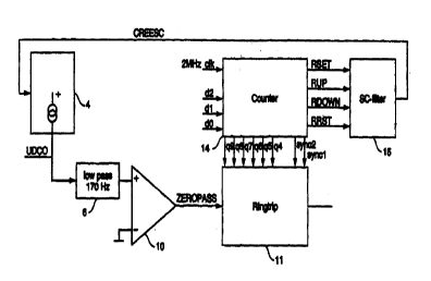
Figure 3 shows that the Ibat generator 4 is controlled by an
input voltage CREFSC and its value is proportional to this input
voltage, zero volt gives zero current and an analog ground given
maximum current. A counter 14 and a 6C-filter 15 achieve a
controlling voltage to the Ibat generator.
The SC-filter 15 is controlled by the counter ~.4, which sends
signals ro the SC-filter to increase, decrease or set the output
voltage.
The counter cycle is divided into the following modes:
- SC-filter steps up the output voltage.
- SC-filter sets the output voltage to a maximum value.
- SC-filter steps dov~rn the output voltage.
- 8c-filter sets the output voltage to a minimum value.
Each mode has an output signal to control the switch capacitor
filter: RUP, RSET. RDOWN' and RRST.
The input clock, 2 Mhz, is d~.vidod by the countez 14, so that
the counter cycle corresponds to the ring signal cycle. The
counter is u$ed as a reference. The outputs from the reference
counter 14, q9-q4 show the position of the ring cycle. The ring
cycle is controlled by the inputs d2, dl, do from a device
processor, which sets the ring sigzzal on or off.
The riagtrip detector 11 is provided with the outputs q9-q4 of
the reference counter 14 and the output from the comparator 10,
which feed8 zero passing. When the ringtrip detector has
indicated a ring trip, the output sets active and passes to the
device processor.
CA 02274525 1999-06-09
26.MRJ.1999 13:28 DEPRRTMENT FOR IPR NR.697 S.11di2b
WO 98IZ6573 PCT/SE971b1937
7
Figure ~ shows the battery current wave form, Ibat , creating a
ring signal on the line wires A and 8. The digital signals q9-q4
represent the outputs of the re~erencc counter of the battery
current generator. Its purpose is to steer the battery current.
The signal sync 1 is used for the positive zero passes and sync2
respectively for the negative zero passes. These signals from
the reference counter ate used to reset the counters and load
the previous counter value into a memory. UDCO is an internal
node of the DC loop) its phase relative to the battery current
generator is response to the load of the line. The continuous
line shows -9o degrees phase respectively +9o degrees far the
dotted line. These lines show the maximum variation of the phase
shift. The 'current zbat is a reference to measure the zero
passes of the line current.
Z5 When the UDCO signal, which corresponds to the line current, is
passing the analog grouad, the zero pass relative to the
reference current Ibat is sensed. There is a digital measurement
of the zero pass relative'to Ibat. The outputs of the reference
counter to Ibatwill be loaded '~.nto registers, when UDCO is
2o passing the analog ground, both at~the negative and the positive
zero passing.
Figure 5 shows the ringtrip deteetot 11 in greater detail. The
output signal ZEItOPASS from the coatparator to is connected to
the D-flipflop DFF, which is clocked by 2 Mhz signal and
25 connected to the inverter INV. The outputs of the inverter and
the D-flipflop are coruiected to a NOR gate and co a AND gate,
which create a pulse at the positive zero pass ZPASSPOS
respectively a pulse at the negative zero pass ZPASSNEC3.
The latches L1 and L2 load the outputs of the reference counter,
3o which control$ the battery current generator) when the pulse four
CA 02274525 1999-06-09
26.MRJ.1999 13:29 DEPRRTMENT F~ IPR , NR.68~ S.11i20
WO 9sI265?3 PCTBE97AD193'7
the positive zero pass respectively the pulse for the negative
zero pass appear during the present ring cycle.The phase of the
signal UDCO can be up to +/-90 degrees relative to the battery
currant Ibat dependent on the line load. The sync signal 9YNC1
S respectively SYNC2) which are 180 degrees to the battery
current, loads the outputs of latch LI. to latch L11 respectively
the outputs of latch L2 to latch L2Z. Tnihen the sync signal
appears a new ring cycle is started and the latches L11 arid LZ2
store the outputs of the reference counter of the previous ring
l0 cycle for the positive zero pass respectively the negative zero
pass. The outputs of the latches L11 and L22 are connected to
each digital comparator C1 sad C2. When the reference counter
passes the values of the previous ring cycle, another pulse
appears at the output of the digital comparators C1 and C2. The
15 difference of the zero passes between the previous and the
pz~asent ring cycles is measured by the counter CE1 for the
positive zero passes respectively the counter C82 for the
negative zero passes. The first zero pass of the present or the
previous ring cycles starts the counter CE1 and the last zero
2o pass stops the counte7r CE1 for the positive zero passes and
respectively CE2 for the negative zero passes. If the zero pass
difference between the prement and the previous ring cycles is
greater than a fixed value, the output will indicate a "phase
difference" and if it is less than the fixed value it will
25 indicate "no phase difference~. The SYNC1 signal clears the
counter CE1 sad the S'YNC2 signal clears the counter CE2 at each
ring cycle.
During each ring cycle, the zero passes relative to the battery
3o current Ibat will be measured at both the positive and the
negative zero passing. It is enough chat one of these
CA 02274525 1999-06-09
~b.MRJ.1999 13:~y L~F'HkIMENT FOR IPR
NK. btll 5. lG~Gd
WO 98126573 PCT1SE97/OI93'f
9
measurements shows phase di~fetenae, so that this cycle
indicates phase difference to counter RT. The outputs of the
councezs CE1 and CE2 ate connected to a counter RT. The made
input of this counter is connected to the output of an RS-
flipflop RS1, the R input of the R8-flipflop is connected to the
RINC3BURSTN signal, which resets the RS-flip~lop at the start of
the ring burst signal. when the RS-flipflop is cleared, the qs
output of the counter RT goes high, when a predererrnined
successive number of ~no phase difference" zero passes has been
to reached. The ring signal zero passes are established and the
counter RT counts successive "phase difference" cycles. When the
counter has reached another predetermined value) the output qe
of the counter goes high. The output ge is connected to another
R6-flipflop RS2) which sets high. The ci=cuit send a zingtip
message to the device processor.
Before the circuit is set to the ring burst mode, the RS-
flipflop RS1 and RS2 ate pleated by a RINGBURSTN signal.
While the foregoing description includes numerous details and
ZO speciiicities, it is to be understood that these are merely
illustrative of the present invention, and axe not to be
construed as limitations, Many modifications will be readily
apparent to those skilled in the art which do not depart from
the spirit and scope of the invention, as defined by the
appended claims and their legal equivalence.
CA 02274525 1999-06-09