Note: Descriptions are shown in the official language in which they were submitted.
CA 02274568 1999-06-09
WO 98/29771 PCT/US97/08064
1
FLEXIBLE OPTICAL CIRCUIT APPLIOUES
BACKGROUND OF THE INVENTION
The present invention relates to flexible optical circuits. In particular, the
present invention relates to flexible optical circuits having a backing layer,
an
adhesive coating and a release liner for attachment to a substrate such as an
electronic printed circuit board.
The design of electronic circuits requires interconnections between devices
to for proper operation. With increased sophistication and operation speeds,
design
of functional interconnections requires careful engineering. The fastest data
processing circuits and emerging technologies require large numbers of
interconnects capable of carrying extremely high speed digital signals. Due to
the
increasing push for higher and higher speeds, engineers are facing fundamental
limits in designing electronic interconnects.
In an attempt to handle higher speeds, interconnection technology has
turned to optical interconnects for next generation circuits. Optical circuits
have
bandwidth capabilities orders of magnitude beyond electrical circuits, and are
inherently immune to electrical interference. In some known designs, discrete
2o fiber optic cables and fiber bundles are used to interconnect devices.
Known
standard fiber optic connection technology employed to connect optical fibers
to
devices are adequate for small numbers of interconnections. However, as
optical
circuit density grows, the physical bulk of cables and connectors make this
approach unwieldy, especially for compact designs.
Attempts have been made to incorporate optical interconnects onto the
surface of electronic circuit boards and substrates by constructing wave
guides
using optical polymers coated to the surface. An example of this is found in
U. S.
Patent No. 5,521,992 to Chun, et al. The technology of the '992 patent
requires
highly specialized tooling to generate each custom optical circuit thus
standard
3o circuit boards cannot be used. For simple circuits, tooling costs may be
prohibitive. Waveguide fabrication is also difficult due to the small geometry
of
the guide regions, and optical quality of finished wave guides is poor due to
limitations in optical polymer chemistry.
CA 02274568 1999-06-09
WO 98/29771 PCT/US97/08064
2
Flexible optical interconnect circuit packs are also known in the art. An
example of this is found in U.S. Patent No. 5,204,925 to Bonanni, et al. The
known optical interconnect circuits have optical fibers bonded between two
flexible substrates and have one or more optical connectors connected along
the
edges of the circuit pack. The connectors are then connected to one or more
optical devices. These known devices are not adapted to bond to a substrate or
circuit board.
The concept of using high bond strength pressure sensitive adhesive coated
laminating films is not new. However, there are certain problems associated
with
to the known adhesive coated films. For instance, it is often difficult to
obtain
accurate positioning during film use. Improper placement, static charge, and
accidental contact can all contribute to misalignment and immediate bonding to
the surface in undesired positions. Because of the immediate aggressive
bonding,
if alignment is off, the film is often destroyed or seriously damaged
attempting to
remove the film for repositioning.
One known solution to the above problem is to use a less aggressive
adhesive so the user may remove or reposition the film in case of
misalignment.
This can result in poor long term adhesion. Another known solution is to use a
partially cured adhesive material followed by a final curing process. This not
only
2o results in additional process step, but may be impractical for many
applications.
Yet another known solution is to prepare a surface wetted with a material that
interferes with adhesion and then removing the wetting agent after final
alignment
is achieved. This approach can be messy and adds process steps.
There is a continuing need for flexible optical circuits capable of being
2s applied to new circuit board designs without changing board design and
fabrication techniques. There is also a continued need for a laminating film
that
allows for repositioning of the optical circuits to achieve proper alignment.
SUMMARY OF THE INVENTION
The present invention provides a flexible optical circuit applique that can
3o be mounted on a circuit board without modifying the circuit board substrate
or the
electronic circuits. The optical circuit applique of the present invention is
also
CA 02274568 1999-06-09
WO 98/29771 PCT/US97/08064
3
repositionable. A method of manufacturing flexible optical circuit appliques
is
also provided.
A preformed fiber optic applique is provided having a backing layer. The
backing layer or film, has an adhesive coating applied thereon. At least one
optical fiber is routed and bonded to the adhesive layer providing a
continuous
optical signal path from one end to another. A releasable liner is releasably
attached to the adhesive layer and positioned to cover the backing layer
including
the at least one optical fiber.
In one embodiment of the present invention, microstructures are provided
on the backing layer. The microstructures are crushable structures that
prevent
the adhesive coating from immediately adhering to a substrate. This allows the
film to be repositioned until proper alignment has been achieved. Upon the
application of appropriate force, the microstructures will crush allowing the
adhesive coating to bond the film to the substrate.
A method of fabricating the fiber optic appliques of the present invention is
also disclosed. The method includes the steps of providing a supply of backing
layer and applying an adhesive coating to the backing layer. At least one
fiber is
then provided and placed on the adhesive coating. Pressure is then applied to
the
at least one fiber to secure it to the backing layer.
2o BRTEF DESCRIPTION OF THE DRAWINGS
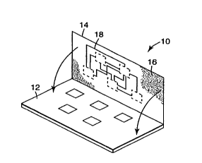
Figure 1 is an exploded perspective view of an electrical circuit board and
a flexible optical circuit applique according to the present invention.
Figure 2a illustrates a preferred method of fabricating an optical circuit
applique according to the present invention.
Figure 2b illustrates an alternative method of fabricating an optical circuit
applique according to the present invention.
Figures 3a, b, c, and d illustrate alternative embodiments of a continuous
web with fibers available for connectorization.
Figures 4a, b, and c illustrate standard sections of optical circuit appliques
3o according to the present invention.
CA 02274568 1999-06-09
WO 98/29771 PCTlUS97/08064
4
Figures Sa and b are top and side plan views of the flexible optical circuit
having microreplicated structures according to the present invention.
Figures 6a and b are top and side plan views of the flexible optical circuits
of Figures Sa and b having optical fibers placed thereon.
Figures 7a, b, c and d illustrate steps in a method for fabricating a flexible
optical circuit and terminating the optical connectors at sockets according to
the
present mvent~on.
Figure 8 is a cross sectional view of a first alternative embodiment of the
present invention.
to Figure 9 is a cross sectional view of a second alternative embodiment of
the present invention.
Figure 10 is a cross sectional view of a third alternative embodiment of the
present invention.
DETAILED DESCRIPTION OF THE INVENTION
The present invention provides a flexible optical circuit applique having a
flexible backing with fibers bonded thereto covered by a releasable liner. The
optical appliques are intended to provide an easy means for adding optical
circuits
to electronic circuit boards or other substrates by laminating. The flexible
optical
circuits of the present invention can also be incorporated into new board
designs
2o without changing standard board design and fabrication techniques. The
optical
appliques of the present invention are also repositionable on a substrate
prior to
bonding.
Figure 1 is a perspective view of a preferred embodiment of a flexible
optical circuit applique 10 according to the present invention. Also
illustrated is a
printed circuit board 12 to which applique 10 is to be mounted. Applique 10
comprises a durable backing material 14 that is coated with a temporarily
repositionable adhesive 16. Applique 10 also includes optical fibers 18 bonded
to
backing 14 via adhesive 16. The particular backing material used depends upon
the particular application. For instance, if high durability is desired, a
polyester-
type backing would be used. If the applique is to be mounted on a curved
CA 02274568 1999-06-09
WO 98/29771 PCT/tTS97/08064
_
substrate, a flexible backing material would be chosen. Examples of backing
materials include vinyl, polyurethane, polyamide, and polyester.
Adhesive 16 of the present invention is any temporarily repositionable
adhesive. By temporarily repositionable, it is meant that the bond between the
5 adhesive and the substrate is such that the material having the adhesive may
be
removed from the substrate without damaging either for a period of time or
until
the occurrence of a specified event which then permanently adheres the backing
to
the substrate. In the preferred embodiment, adhesive 16 is preferably a
pressure
sensitive adhesive. Pressure sensitive adhesives are known in the industry as
a
to standard class of materials. They are adhesives, which in dry form
(substantially
solvent free except for residual solvent) are aggressively and permanently
tacky at
room temperature (approximately 15° to 25° C) and firmly adhere
to a variety of
similar surfaces upon mere contact without the need for more than manual
pressure. The adhesives require no activation by water, solvent, or heat in
order
to exert a strong adhesive holding force towards such materials as paper,
cellophane, glass, plastic, wood, and metals. The adhesives have a
sufficiently
cohesive holding and elastic nature such that, despite their aggressive
tackiness, it
can be handled with fingers and removed from smooth surfaces without leaving a
substantial residue. For a more detailed discussion of pressure sensitive
adhesives,
reference should be made to U.S. Patent Nos. 5,296,277, 5,362,516 and
5,449,540, which are assigned to the Assignee of the present invention.
If adhesive 16 has low tack, e.g. is only slightly sticky to the touch and
has low adhesion to certain types of surfaces, a release liner may not be
required
to cover the adhesive layer, and the backing material 14 may act as a release
liner
when the film is rolled.
A light cured adhesive could be used with a transparent backing layer
without departing from the spirit or scope of the invention. Such an adhesive
would allow the film to be repositioned on a substrate until a light source,
typically
an ultra violet light, is applied through the transparent film which would
then
3o activate the adhesive to secure the film to the substrate. Nonpressure
sensitive
adhesives, thermally activated adhesives such as hot melt glue or solvent
activated
CA 02274568 1999-06-09
WO 98/29771 PCT/LTS97/08064
6
adhesives could also be used if desired, without departing from the spirit or
scope
of the invention. They are, however, less preferred embodiments because of the
additional application steps and greater tendency to entrap air during
application.
Optical fibers 18 of the present invention are preferably 80 to 100 micron
glass (silica) diameter fibers with a special fiber coating described in U.S.
Patent
No. 5,381,504. Standard glass optical fibers have 125 micron outside
diameters.
By using glass fibers with diameters of 80 to 100 microns, the present
invention
can obtain bend radiuses as small as 0.25 inches (0.64 cm) while staying below
a
bending stress of 100 K psi. At a bend radius of 0.25 inches (0.64 cm), a
fiber
1o having a diameter of 125 microns has a bending stress of approximately 110
K psi
and a fiber having a diameter of 200 microns has a bending stress of
approximately
175 K psi. In the preferred embodiment of the present invention, bend radii of
less
than 0.3 inches (0.76 cm) are achieved at bend stresses of less than 100 K
psi.
Figure 2a illustrates a preferred method of fabricating an applique
according to the present invention. A supply roll 20 of applique backing layer
or
film, 14 is provided, as is a takeup roll 22. Film 14 is precoated with an
adhesive
layer 16 and covered with a releasable liner 17. A second takeup roller 19 is
provided to take away releasable liner 17 as illustrated. A rotating drum 24
is
provided to move backing film 14 from supply roll 20 to takeup roll 22.
Multiple
2o spools 28 of fibers 18 are provided and are suspended above backing film
14. A
laminating roll spacing guide 30 is provided to space fibers 18 as desired and
to
press the fibers onto backing film 14 with sufficient force to activate
pressure
sensitive adhesive 16 to bond fibers 18 in place. A second supply roller 32 is
provided carrying a second releasable liner 34 which releasably adheres to
pressure sensitive adhesive 16. It should be noted that film 14 may be a
continuous and solid film or it may have holes formed therethrough for
connectorization with optical circuit components, as will be described in
greater
detail below.
Figure 2b illustrates an alternative method of fabricating an applique
3o according to the present invention. Figure 2b is similar to Figure 2a and
thus like
elements are correspondingly identified. Supply roll 20 of applique backing
film
CA 02274568 1999-06-09
WO 98/29771 PCT/LTS97/08064
7 _
14 is provided as is takeup roll 22. Rotating drum 24 is provided to move
backing
film 14 from supply roll 20 to takeup roll 22. A pressure sensitive adhesive
coating device 26 is provided to apply a coating of pressure sensitive
adhesive 16
to backing film 14 as the backing film comes off of supply roll 20. Multiple
spools
28 of fibers 18 are provided and are suspended above backing film 14.
Laminating
roll spacing guide 30 is provided to space fibers I8 as desired and to press
the
fibers onto backing film 14 with sufficient force to activate pressure
sensitive
adhesive 16 to bond fibers I8 in place. Second supply roller 32 is provided
carrying release liner 34 which releasably adheres to pressure sensitive
adhesive
l0 16.
Fabricating appliques in a continuous web process, as illustrated in Figures
2a and 2b is a very cost effective way to fabricate the appliques. Depending
upon
the length of appliques desired, large numbers of standard appliques can
easily be
made from a single roll of backing film 14.
1s Figures 3a - 3d illustrate alternative ways to make fibers 18 available for
connectorization in a continuous web process similar to those described in
Figures
2a and Zb above. It should be noted that the examples given below are given
only
as exemplary ways to avail the fibers for connectorization, and the examples
given
are not meant to be an exhaustive list. The illustrations in Figures 3a-3d use
some
20 of the same components as used in Figures I and 2, therefore, like elements
will be
correspondingly identified. In Figure 3 a, film 14 is coated with adhesive
layer 16.
Fibers 18 are bonded to adhesive layer 16 as previously described. A release
strip
35 is provided across the width of film 14 at predetermined intervals. The web
is
then cut at release strips 3 5. When applied to a substrate, release strips 3
5 prevent
25 the ends of the individual applique section from adhering to the substrate
thus
allowing the ends of the fibers to be prepared for connectorization. It should
be
noted that release strip 35 not need to extend across the entire width of film
14.
In Figure 3b, a series of receiving cavities 37 are formed through film 14.
The
receiving cavities allow access to fibers 18 when the applique is adhered to a
3o substrate.
CA 02274568 1999-06-09
WO 98/29771 PCT/LTS97108064
8 _
Figure 3c illustrates a series of mechanical alignment devices 39 spaced at
desired locations along the continuous web. Alignment devices 39 provide
mechanical alignment for fibers 18 and also function as release liners.
Mechanical
alignment devices 39 are preferably V grooved structures, but may also be U
shaped or other shapes that provide adequate alignment for fibers 18. After
fibers
18 have been adhered to adhesive surface 16 of film 14, alignment device 39
may
be removed prior to adhering to a substrate. Alignment device 39 could also be
left in place with the applique adhered to a substrate. A connector assembly
is
then mounted around the fibers. In Figure 3 d, an adhesiveless area 41 is
provided
to on film 14. Thus, when film 14 is adhered to substrate, fibers 18 are not
adhered
to the substrate in adhesiveless area 41.
The design of the applique according to the present invention including the
number of fibers, the spacing of the fibers as well as the routing patterns
can be
done during the manufacturing process using a simple process control computer
software program. Therefore, a board designer may layout a board and provide
the manufacturer of the appliques of the present invention a layout of the
board
and an applique may be quickly and easily laid out by the process control
program.
Design and manufacture of appliques of the present invention may be conducted
by, for example, Icon Industries, Euless, TX.
2o Figures 4a, b and c illustrate some standard applique constructions. Figure
4a illustrates a 180° bend applique 36. Figure 4b illustrates a
90° bend applique
3 8 and Figure 4c illustrates a straight applique 40. Additional standard
applique
constructions besides the ones illustrated in Figures 4a-c, such as 30°
bends, 60°
bends, 45° bends etc., are also considered within the spirit and scope
of the
present invention. Additionally a continuous web construction having
alternating
patterns may be formed. Standard appliques such as those discussed above can
be
premade and purchased ready to use. Because the appliques of Figures 4a-c may
be purchased as ready to use appliques, the ends of fibers 18 are also
prepared for
connectonzation.
3o It should be noted that the fibers illustrated in Figures 4a-4c are shown
stopping at the edge of the backing material. However, the fibers must be
CA 02274568 1999-06-09
WO 98/29771 PCT/iJS97/08064
9
available for connectorization. Thus, any of the methods for making fibers
available for connectorization, such as those described with respect to
Figures 3a-
3d, may be utilized.
Appliques 10 can be applied to circuit boards 12 or other substrates by
users during the manufacturing process, by removing release liners 34 (not
shown
in Figures 4a, 4b or 4c) from the adhesive surface and laminating the applique
to
the circuit board surface. It should be noted that multiple appliques can be
placed
over one another without degrading performance.
Figures Sa and b illustrate top and side plan views of flexible optical
circuit
to applique 10 incorporating microreplicated structures 42 formed on backing
film 14
or in adhesive surface 16. Microreplicated structures 42 are provided to allow
accurate positioning of applique 10. Improper placement or accidental contact
of
an active adhesive surface can contribute to misalignment and immediate
bonding
to the desired surface. Because the microstructures protrude up from backing
film
14 and are taller than the depth of adhesive coating 16, microstructures 42
prevent
intimate contact between adhesive surface 16 and circuit board 12 or other
mounting surface. Structures 42 are crushable such that intimate contact
between
adhesive surface 16 and circuit board I2 is obtained when suitable pressure is
applied. Thus, the present invention may be repositioned until accurate
alignment
2o is achieved and fi~rther provides a high final bond strength after
lamination. The
microreplicated structures of the present invention are preferably
approximately
I5 micrometers high. Additionally, the density or durometer of structures 42
can
be varied to provide lesser or greater resistance to crushing or forming. For
a
more detailed description of microstructures 42, reference should be made to
the
above mentioned U.S. Patent Nos. 5,296,277, 5,362,516 and 5,449,540. It should
be noted that alternative embodiments of microstructures 42 or other
repositionable adhesive constructions are also considered within the spirit
and
scope of the present invention. For instance, the adhesive may contain
microspheres which may house a catalyst, either with or without the presence
of
3o microstructures 42, such that when sufficient force is applied, the
microspheres,
CA 02274568 1999-06-09
WO 98/29771 PCT/US97/08064
and microstructures if present, are crushed and the catalyst is released,
reacting
with adhesive 16 to form an aggressive adhesive.
Figures 6a and b illustrate an applique having microstructures 42 arranged
in desired patterns such that microreplicated structures 42 provide a guide
for
5 routing fibers 18 in precise locations when bonded to adhesive surface 16.
As
illustrated in Figures 6a and 6b, fibers 18 fit into channels 44 between
structures
42 and may thus be bonded to adhesive surface 16 without crushing structures
42.
As previously stated, the microstructures may be positioned as described to
form
any such pattern.
to Microstructures 42 may be formed on backing film 14 before applying
adhesive coating I6. Or, they may be added to adhesive surface 16 after
applique
10 is constructed and fibers 18 are bonded to film 14 by having
microstructures 42
picked up from an embossed release liner 34 which is attached immediately
after
fabrication.
Figures 7a-d illustrate steps for fabricating an applique according to the
present invention that terminates fibers 18 in sockets or connectors. To
facilitate
the fabrication process, a multichip module positioning fixture 52 is provided
to
give support to backing film 14 and to provide a pattern for cutting out
receiving
cavities where sockets are inserted.
2o One preferred method of fabricating an applique according to the present
invention having sockets inserted therein is described below. It should be
noted
that the below described method is given as one example and should not be
considered the only way to fabricate an applique according to the present
invention. Backing film 14 is unspooled and placed over positioning fixture 52
as
illustrated in Figure 7a. Pressure sensitive adhesive 16 is either applied to
backing
film 14 or backing film 14 already has an adhesive layer coating thereon.
Optical
fibers 18 are then routed to desired positions on backing film 14. The paths
taken
by fibers 18 may follow parallel or individual routes, and provide a
continuous
signal path from one end to another. The optical circuit paths may also cross
3o previously installed fibers producing multiple layers to optimize path
geometry.
Once fibers 18 are routed appropriately, they are bonded to backing film 14 by
CA 02274568 1999-06-09
WO 98/29771 PCT/US97108064
11
applying sufficient force to activate pressure sensitive adhesive 16. At this
point,
backing film 14 is cut at positions 49 where sockets are to be installed. As
shown
in Fig. 7b, the ends of fibers 18 are then cut, cleaved, sawed, polished or
otherwise prepared for termination depending on user requirements. For ease of
connectorization, optical fibers 18 are usually terminated in connectors or
sockets
50. After preparing fiber ends, socket 50 is inserted through the hole formed
in
backing film 14 (Fig. 7c). Finally, as shown in Fig. 7d, a circuit board or
other
substrate 12 is bonded to backing film 14 and the backing film is cut to fit
in the
circuit board.
to The appliques of the present invention allow the optical paths formed by
fibers 18 to be pretested before applying to circuit board 12 or any other
substrate.
Another benefit of the present invention is that fibers 18 are protected by
film 14
when applied to circuit board 12. As previously stated, the backing film may
vary
depending upon the application. If greater protection for fibers 18 is needed,
a
stronger or thicker backing may be chosen. A further benefit of the appliques
of
the present invention is that the risk of damaging a valuable circuit board is
greatly
reduced. Typically, there is already substantial value invested in a circuit
board at
the time of providing electrical or optical connections. Using the present
invention, the circuit boards do not need to be destroyed if proper alignment
is not
2o achieved or if the applique is not working. If waveguides are used and a
mistake
is made, the circuit board is usually ruined.
Figure 8 illustrates an alternative embodiment of an applique 68 according
to the present invention. As stated above, backing film 14 protects fibers 18
when
applied to circuit board 12. However, it may be desirable to have a protecting
film
between fibers 18 and board 12. Thus, as illustrated in Figure 8, a first
backing
film 60 is provided having a top surface 62 and a bottom surface 64. A first
adhesive layer 66 is provided on bottom surface 64. A second backing film 69
is
provided having a top surface 70 and a bottom surface 72. A second adhesive
layer 74 is provided on bottom surface 74. At least one optical fiber 76 is
3o sandwiched between backing films 60 and 68. Applique 68 is then mounted to
a
substrate such as a circuit board and bonded in place with adhesive 74. As
with
CA 02274568 1999-06-09
WO 98/29771 PCT/US97/08064
12
the embodiment described above, microstructures (not shown in Figure 8) could
also be included to allow for repositionability or fiber alignment.
Figure 9 illustrates a further alternative embodiment of an applique 79
according to the present invention. A backing layer or film 80 is provided
having
a top surface 82 and a bottom surface 84. An adhesive 86, such as a hot melt
adhesive, is provided on top surface 82. At least one optical fiber (not
shown)
may be bonded to top surface 82 via adhesive 86. A second adhesive layer 90 is
provided on bottom surface 84. Preferably adhesive layer 90 is a pressure
sensitive adhesive that allows repositionability. Microstructure 92, similar
to
1o those described above, may also be provided on bottom surface 84. Applique
79
is designed to mount on a substrate, such as a circuit board, with bottom
surface
84 being adhered to the substrate with adhesive layer 90.
Figure 10 illustrates a further alternative embodiment of an applique 100
according to the present invention. A cover layer or film 101 is provided
having a
top surface IOIA and a bottom surface lOIB. A backing layer or film 105 is
provided having a top surface lOSA and a bottom surface lOSB. An adhesive 106
such as a hot melt adhesive or a pressure sensitive adhesive, is provided on
top
surface lOSA of the backing layer 105. At least one optical fiber 108 is
bonded
between bottom surface lOIB of the cover layer 101 and top surface IOSA of
2o backing layer 105 via adhesive 106. The bottom surface lOIB of the cover
layer
101 is provided with fiber alignment microstructure 103 which ensures proper
positioning of the at least one optical fiber 108. Alternatively, such fiber
alignment microstructure could be provided on top surface lOSA of the backing
layer. A second adhesive layer 110 is provided on bottom surface lOSB of the
backing layer. Preferably, adhesive layer 110 is a pressure sensitive adhesive
that
allows repositionability. Crushable microstructure 112, similar to those
described
above, may also be provided on bottom surface lOSB to enhance
repositionability.
Applique 100 is designed to mount on a substrate, such as a circuit board,
with
bottom surface lOSB being adhered to the substrate with adhesive layer 110.
CA 02274568 1999-06-09
WO 98/29771 PCT/US97/08064
13
Although a certain preferred embodiment has been shown and described, it
should be understood that many changes and modifications could be made therein
without departing from the spirit or scope of the appending claims.
SUBSTITUTE SHEET (RULE 26)