Note: Descriptions are shown in the official language in which they were submitted.
CA 02274577 1999-06-09
WO 98125749 PCT/US97/22593
_ 1
INJECTION MOLDING ENCAPSULATION
FOR AN ELECTRONIC DEVICE DIRECTLY ONTO A SUBSTRATE
BACKGROUND
' The invention relates to plastic encapsulation of
electronic devices, and more specifically, to injection
molding an encapsulation for an electronic device
directly onto a substrate such as a printed circuit
board.
It is well known that electronic devices are
sensitive to the environment and that exposure to normal
atmospheric conditions may degrade or ruin them entirely.
Accordingly, it is the current practice to protect
electronic devices from environmental/atmospheric
exposure by sealing them within a protective enclosure,
commonly made of a non-electrically conducting material
such as a plastic resin, with an interfacing means, such
as pins, to allow connection of the devices to a larger
electronic circuit or other devices. Simple devices such
as resistors, capacitors, diodes and the like, as well as
more complex semiconductor devices, or chips, are
commonly packaged in this manner.
It is common practice to interface such an
encapsulated device with other devices mounted on a
supporting substrate by, for example, inserting its
interface pins into a corresponding socket mounted on the
substrate. These other devices are similarly mounted and
connected to each other with wires, or with traces in the
case where the substrate is a printed circuit board.
This practice of encapsulation suffers from a
number of drawbacks. Generally, the equipment and
materials necessary to accomplish the encapsulation must
be located outside of the clean room environment where
the device itself is manufactured, and the encapsulation
must therefore be performed as a separate manufacturing
CA 02274577 1999-06-09
WO 98!25749 PCTIL1S97122593
- 2 -
step. The encapsulating process is also expensive.
Further, the plastic packages themselves, with the
required interface means, significantly increase the size
of the device, thereby requiring a larger area, or more
real estate, for their incorporation in another device or
circuit.
Alternatively, it is known that certain electronic
devices may be mounted to a substrate such as a printed
circuit board, typically with gold wire connections, and
encapsulated by a liquid resin that is hand cast over the
device on the substrate. This procedure is not preferred
because it is expensive, time-consuming, difficult to
accurately place the cast material over the device, and
provides poor adhesion of the cast material to the
substrate. Further, the gold wire connections to the
device are very delicate and are easily disconnected
during the casting process.
Another prior-art method for encapsulating devices
mounted onto a substrate by gold wires is the so-called
"transfer molding" method. Transfer molding is a process
by which a thermosetting material is caused to flow into
a cavity formed by the cooperation of a mold and a cavity
plate. The material enters the cavity through so-called
"side" gates which are also formed by the space between
the cavity plate and the mold. This method is an
improvement over the hand-casting encapsulation method
because it allows multiple devices to be encapsulated at
the same time in one production cycle and it allows for
somewhat more accurate placement and size of the
resulting encapsulated package.
Transfer molding, however, itself suffers from a
number of significant drawbacks which are eliminated by
the present invention. Initially, transfer molding
techniques of encapsulating electronic devices are
limited to use of thermosetting materials which have a
CA 02274577 1999-06-09
WO 98125749 PCTIUS97/22593
- 3 -
low viscosity. Such a material is necessary to prevent
damage to the delicate connections of the device to the
substrate during the molding process. This same danger
requires that the encapsulating material be forced into
the mold at low pressure. Use of a low viscosity
thermoset results in the need for an expensive mold
apparatus which must be constructed with very high
tolerances to prevent leakage of the encapsulating
material. Even the most expensive molds, however,
exhibit some leakage in the area of the gate and device
connections which must be removed by additional process
steps after molding, thereby increasing cycle times.
Use of a thermoset, which cures by a chemical
process, also results in long cycle times, on the order
of 5 to 15 minutes, which increases production costs.
Thermoset materials themselves are expensive due, in
part, to the inability to reuse excess encapsulating
material resulting from the molding process after the
material has cured.
Use of a low viscosity thermoset at low insertion
pressure also results in the need for large side entry
gates for the encapsulating material. The large side
gates make transfer molding impractical for small devices
because the size of the gate limits the size of the
cavity. The gating used in transfer molding techniques
adds further limitations to the placement and
configuration of the devices to be encapsulated because
it requires the devices to be near an edge of the
substrate to which it is to be bonded. Typical transfer
molding applications therefore involve devices which are
mounted in a linear arrangement on a substrate with the
use of strip-like carriers, or "lead frames," for the
devices. Transfer molding with thermosets is also not
useful with small devices because the thermosetting
material requires substantial surface area in contact
a n
CA 02274577 1999-06-09
WO 98125749 PCT/US97/22593
- 4 -
with the substrate in order to adhere sufficiently to
hold the device and encapsulate to the substrate with a
chemical or adhesive bond.
On the other hand, use of higher viscosity
thermoplastic materials is not practical in transfer
molding because it requires higher pressures that may
damage the device connections and may result in
additional leakage of the encapsulating material.
Further it is difficult in a transfer molding apparatus
l0 to maintain the high temperatures required to allow a
thermoplastic material to properly flow.
Attempts have been made to solve the problems with
prior-art encapsulating methods by use of injection
molding. Prior art injection molding methods, however,
suffered from similar drawbacks. Although higher
pressures may be used with injection molding and thus
would allow use of thermoplastic materials, the injection
process would damage the delicate device connections. In
addition, prior art injection molding methods and devices
were not useful for small devices because the smaller
gating necessitated by smaller cavities had a tendency to
clog with the thermoplastic material and this material
exhibited poor adhesion resulting in devices being
separated from the substrate.
SUMMARY
In general, in one aspect, the invention features
a method of encapsulating a small electronic device
mounted directly on a substrate by providing a three-
dimensional formation on the substrate adjacent to the
device and injection molding a thermoplastic
encapsulating material to cover the device and extend
over the three-dimensional formation on the substrate and
wherein the encapsulating material mechanically bonds to
the three-dimensional formation. In another aspect, the
invention features a method of encapsulating a light
CA 02274577 1999-06-09
WO 98/25749 PCT1US97J22593
- 5 -
emitting diode (LED) mounted directly on a substrate by
providing a hole through the substrate adjacent to the
~ LED and injection molding a light-transmissive
thermoplastic encapsulating material to cover the LED and
~ 5 fill the hole. In another aspect the invention features
a method of encapsulating a set of LEDs mounted directly
to a printed circuit board (PCB) and arranged to form an
alphanumeric display by providing a hole through the PCB
adjacent to each of the LEDs, injection molding a light-
transmissive thermoplastic around each of the LEDs and
wherein each of the LEDs is separately encapsulated in a
package that is shaped to focus and reflect light from
the LED and is mechanically bonded to the PCB. In a
further aspect, the invention features a method of
encapsulating a plurality of small electronic devices
mounted directly on a substrate in close proximity to one
another comprising providing a three-dimensional
formation on the substrate adjacent to each device,
injection molding a thermoplastic encapsulating material
to individually cover each device and wherein the
encapsulating material mechanically bonds to the three-
dimensional formation on the substrate.
In another aspect the invention features a mold
for injection molding a thermoplastic encapsulating
material over a small electronic device mounted directly
on a substrate, the mold comprising a base member, a top
member including an inlet, and a gate plate including a
short gate having an input communicating with the inlet
and an output communicating with a cavity, and wherein
the gate is formed entirely within the gate plate. In
another aspect the invention features a gate plate for
use in injection molding a thermoplastic encapsulating
material over a small electronic device mounted directly
on a substrate comprising a cavity formed to enclose the
device, and a short gate having an input for receiving an
CA 02274577 1999-06-09
WO 98/25749 PCTIUS97122593
- 6 -
encapsulating material and an output communicating with
the cavity, and wherein the gate is formed entirely
within the gate plate. In a further aspect, the
invention features a gate plate for use in injection
molding a light-transmissive thermoplastic encapsulating
material over a set of LEDs mounted directly on a
substrate comprising a set of cavities arranged in the
form of an alphanumeric display, each cavity formed to
enclose one LED and extend over its adjacent hole and a
set of short conical gates, each having an input for
receiving an encapsulating material and an output
communicating with a cavity, and wherein the gates are
formed entirely within the gate plate.
In another aspect, the invention features an
encapsulated electrical device mounted directly on a
substrate wherein the device is fully encapsulated by an
encapsulating material which is injection molded onto and
mechanically bonded to the substrate. In a further
aspect, the invention features an alphanumerical display
comprising a set of LEDs mounted directly to a PCB with
holes through the PCB adjacent to each of the LEDs and
arranged to form a display and wherein each of the LEDs
is separately encapsulated in a package of light-
transmissive material that has been molded onto and
mechanically bonded to the PCB.
Preferred embodiments of the invention include one
or more of the following features. A three-dimensional
feature on the substrate adjacent to the device to be
encapsulated where the three-dimensional feature is
optionally a hole, a raised member extending above the
surface of or a groove extending below the surface of the
substrate. A substrate comprising a printed circuit
board. An encapsulating material comprised of a
thermoplastic resin chosen from among the groups of
polycarbonates and acrylics. A method wherein, after
CA 02274577 1999-06-09
- WO 98/25749 PCT/US97122593
injection, the encapsulating material is located on less
than the entire surface of the substrate. Encapsulating
- a light emitting diode in a light-transmissive
encapsulating material. Encapsulating on a PCB a light
emitting diode using a lozenge shaped hole adjacent to
the LED and wherein, after encapsulation, the
encapsulating material on the side of the PCB opposite
from the light emitting diode is substantially flat and
flush with the surface of the printed circuit board.
Encapsulating a plurality of LEDs on a PCB in the form of
an alphanumeric display including, for example, a seven
segment display. Encapsulating a plurality of devices
arranged in a non-uniform arrangement on a substrate and
wherein one or more of the devices are located away from
the edges of the substrate. A gate plate having a
substantially conical gate. A gate having a cross
sectional area that is reduced from the input to the
output to form a region of relatively reduced strength in
hardened encapsulating material, whereby the material is
caused to break off near to the output of the gate when
the mold is opened. A gate having sidewalls that are
inclined about 15 degrees over the length of the gate
from the input to the output. A gate plate about 0.250
inches thick. A gate plate including a distribution
runner connected to the gate. A gate about 0.065 inches
long.
A set of cavities arranged in the form of an
alphanumeric display. A set of cavities arranged in the
form of a seven-segment display. A cavity shaped to form
a package of encapsulating material that focuses and
reflects light from a light emitting diode out of an
adjacent hole in the substrate. A cavity having a base
opposite from the output of the gate, which base is
substantially triangular with rounded corners and which
cavity is substantially rounded above its base. An
CA 02274577 1999-06-09
WO 98/25749 PCT/LTS97/Z2593
_ g _
encapsulated electrical device mounted directly on a
substrate wherein the device is fully encapsulated by an
encapsulating material. An alphanumerical display
comprising an array of light emitting diodes separately
encapsulated in a package of light-transmissive
thermoplastic material.
Among the advantages of the invention are one or
more of the following. The invention eliminates the need
for separate, expensive and time-consuming encapsulation
of electronic devices. The invention eliminates the need
for pin interfaces on circuit boards. The invention
reduces the amount of space required on a circuit board
for a given electronic device. In one aspect, the
invention provides an injection molding method where the
encapsulating material hardens quickly by loss of heat,
without leakage of material, thereby increasing
production speed and capacity. The invention increases
production speed by eliminating the need to mill excess
encapsulating material after molding. The invention
allows for economical reuse and recycling of a
thermoplastic encapsulating material. In another aspect,
the invention provides apparatus for injection molding
that is efficient and economical. In another aspect, the
invention provides an injection mold with a thin gate .
plate that is separate from the larger top and bottom
plates of the mold and that may be designed to be
constructed of relatively inexpensive material and
therefore economically replaced when worn. The invention
further provides an injection molding apparatus that
allows placement of an encapsulating material in any
location and in any configuration on a substrate. In
another aspect the invention provides an injection
molding apparatus that allows many small devices to be
individually encapsulated in close proximity to one
another. The invention alleviates the potential problems
CA 02274577 1999-06-09
WO 98/25749 PCT/US97122593
_ g _
of wires or traces being torn or disconnected from the
device and prevents the device from being separated from
the substrate by making use of small devices that may be
mounted directly to the substrate without wires and by
~ 5 mechanically bonding the encapsulated material to the
substrate. In another aspect, the invention quickly and
economically encapsulates a light emitting diode on a
printed circuit board using a minimum of real estate.
The invention further provides an alphanumeric display
economically constructed on a printed circuit board by
injection molding a separate encapsulation around each of
an array of LEDs mounted directly to the board. Other
features and advantages of the invention will become
apparent from the following description and from the
claims.
BRIEF DESCRIPTION OF THE DRAWINGS
Figure 1 is an exploded view of a mold for
injection molding a package of an encapsulating material
for an electronic device onto a substrate.
Figure 2 is a step-by-step illustration of
injection molding a package of an encapsulating material
onto a substrate bearing an LED.
Figure 2-Z is an exploded view of the mold of
Figure 1 with a substrate in position to be injection
molded.
Figure 2-2a is a detailed view of the substrate of
Figure 2-1.
Figure 2-2b is a more detailed view of a single
LED mounted to the substrate of Figure 2-2.
Figure 2-3 is a detailed view of the substrate of
Figure 2-2 including the molded package.
Figure 2-4a is a section view of the substrate of
Figure 2-3.
CA 02274577 1999-06-09
WO 98/25749 PCTIUS97/22593
- 10 -
Figure 2-4b is a view of an alternate embodiment
of the substrate of Figure 2-3 with a raised member on
the substrate instead of a hole.
Figure 2-5 is a sectional view of the mold of
S Figure 2-1.
Figure 2-6 is an enlarged view of the gate and
cavity of the mold of Figure 2-5.
Figure 2-7 is a view of the top of the gate plate
of the mold of Figure 2-1.
Figure 2-8 is a view of the bottom of the gate
plate of the mold of Figure 2-1.
Figure 2-9 is a detailed view of the cavities and
gates of the gate plate of Figure 2-7.
Figure 2-10 illustrates the removal of excess
encapsulating material.
Figure 2-11 is an enlarged view of the gate and
cavity of the mold of Figure 2-5 shown in place above the
substrate of Figure 2-3 after injection and after the
removal of excess encapsulating material.
Figure 2-12 is an exploded view of the mold of
Figure 2-1 with the package molded to the substrate.
Figure 3 is a diagram of the mold of Figure 1 in
place in an injection molding apparatus.
DETAILED DESCRIPTION
Referring to Figure 1, mold 100 includes top plate
10, gate plate 20 and base plate 40. Top plate 10
includes inlet 11 that provides a path for injecting an
encapsulating material into mold 100. Gate plate 20
includes gates 21, distribution runner 25 and ejection
holes 26. Gates 21 communicate with inlet 11 through
optional distribution runner 25. Alternatively, gates 21
may communicate directly with inlet 11. However, use of
distribution runner 25 improves the flow of an
encapsulating material to gates 21 and facilitates the
CA 02274577 1999-06-09
WO 98/25749 PCTlUS97122593
- 11 -
creation of shorter gates. Base plate 40 includes
ejection pins 41 and locating pins 42.
Referring to Figure 2-1, substrate 30 is
positioned within mold 100 by being placed on base plate
- 5 40 so that locating holes 33 fit over locating pins 42.
Gate plate 20 is placed on top of substrate 30 and top
plate 10 is placed on top of gate plate 20. (Substrate 30
is not part of mold 100) .
Referring to Figure 2-2a, substrate 30 is a
printed circuit board as is well known, and light
emitting diodes ("LEDs") 32 are mounted directly to
substrate 30. Small electronic devices such as LEDs 32
may be mounted directly to substrates without the need
for delicate gold wire connections. The connections may
be made "pad-to-pad", i.e.) between conductive surfaces
on the upper surface of the substrate and on the bottom
surface of the device itself. Mounting of the device
directly to the substrate without delicate gold wires
eliminates the prior art problem of damage to these
connections which occurred during the molding of an
encapsulation.
Substrate 30, additionally includes a three-
dimensional formation adjacent to each LED 32. As shown,
this three-dimensional formation comprises holes 31
through substrate 30. In addition to a printed circuit
board, substrate 30 may, alternatively, be any suitable
electrically insulating material and may be, for example,
a bread-board, a plastic plate, a piece of glass, a
coated metal plate or other mounting surface. In the
specific LED application shown, holes 31 are lozenge
shaped and arranged to form the familiar seven-segment
arrangement of numeric displays. Each LED 32 has a
corresponding hole 31 adjacent to it. Other arrangements
of holes and LEDs may be contemplated that may be used to
form more generalized alphanumeric displays. For
i a
CA 02274577 1999-06-09
WO 98125749 PCT/US97I22593
- 12 -
example, a simple rectangular array or grid of LEDs may
be used to generate a wide variety of characters and the
implementation of such alphanumeric displays is well
known.
Referring to Figure 2-2b LED 32 is connected to
trace 38 which electrically connects LED 32 so LED 32 may
be used as part of a completed circuit. Each LED 32 is
similarly connected~to its own trace 38 formed in
substrate 30 which is a printed circuit board.
Referring to Figure 2-3, after completion of the
encapsulation process, a package of hardened
encapsulating material 34 completely encloses LED 32.
The package of encapsulating material 34 also fills hole
31. Holes 31 promote the bonding of package 34 to
substrate 30. As it hardens, the encapsulating material
shrinks and forms a mechanical bond with the substrate at
hole 31. This mechanical bonding allows for very small
devices to be encapsulated and strongly held to the
substrate. Although shown of a shape and size to form a
seven-segment display, when devices other than LEDs are
being encapsulated, holes 31 need only be of sufficient
number, size and placement to insure adequate bonding of
the encapsulating material. The specific number, size
and placement will be determined, in turn, by the size
and shape of the device being encapsulated.
Figure 2-3 shows that one set of seven LEDs has
been encapsulated. However, the encapsulation of a
single device, several devices, or all the devices on
substrate 30 may be accomplished in one injection cycle.
In practice, a large number of sets of LED 32, on
multiple substrates, will be encapsulated in one
injection cycle.
Substrate 30 may contain any kind of small
electronic device to be encapsulated. LED 32 is shown by
way of example only and the disclosed method and
CA 02274577 1999-06-09
WO 98/25749 PCT/LTS97/22593
- 13 -
apparatus may be used to quickly and economically
injection mold a package of any shape around any kind of
' device that may be directly connected to a substrate.
For example, simple devices such as resisters or
~ 5 capacitors as well as more complex devices such as Random
Access Memory ("RAM"), microprocessors, or any other
electronic devices may be encapsulated in a similar
fashion. The disclosed method and apparatus are
especially useful in encapsulating a number of very small
electronic devices (on the order of approximately 12/1000
inch in diameter and larger) that are to be placed in
close proximity to one another on the same substrate
(within approximately 12/1000 inch from one another and
further apart).
The encapsulation of the device is advantageously
accomplished by mechanically bonding the encapsulating
material directly to the substrate. In one example shown
in Figure 2, this bonding is accomplished by the use of
holes 31 in substrate 30 which retain the encapsulating
material as it shrinks during hardening and promotes the
formation of a mechanical bond. Holes 31 may be of any
shape and may be created through any method, for example,
with a punch, a laser, or by etching, milling or routing
the substrate. An added advantage to using holes 31 in
substrate 30 to aid the encapsulation of LED 32, as
contrasted with other three-dimensional formations
discussed below, is that the LED's 32 light may be
transmitted through the holes 31 from the LED 32 mounted
on the back side of substrate 30.
This mechanical bonding of the encapsulating
material to the substrate may also be promoted by other
three-dimensional formations on the substrate such as,
for example, raised members extending above the surface
of the substrate that "grip" the encapsulating material
as it shrinks during hardening, or recesses extending
CA 02274577 1999-06-09
w WO 98/25749 PCTlUS97/Z2593
- 14 -
below the surface of the substrate that retain the
encapsulating material in a manner similar to that of
holes 31. The mechanical bonding allows for very small
devices to be encapsulated in small packages wherein only
a small contact surface exists between the encapsulating
material and the substrate. Such a small contact
surface, on the other hand, prevents the formation of an
adhesive or chemical bond which has adequate strength
alone to hold a device and package to the substrate.
Referring to Figure 2-4a, the package of hardened
encapsulating material 34 can be more easily seen to
completely enclose LED 32. The package of hardened
encapsulating material 34 also fills in hole 31 and forms
a surface flush with the bottom surface 36 of substrate
30. The shape of the package will be determined by the
shape of the cavity of gate plate 20. The configuration
of these cavities will be discussed in more detail below.
As shown in Figure 2-3, package 34 is substantially
triangular with rounded corners at the surface of
substrate 30 and is rounded as it rises above the surface
to form a roughly semi-spherical shape. The shape and
composition of the package of hardened encapsulating
material 34 also acts to focus and reflect light
transmitted from LED 32 out hole 31. In an application
using an LED, this configuration allows the bottom
surface 36 of substrate 30 to be the "face" of the device
and provide a desireable flat display.
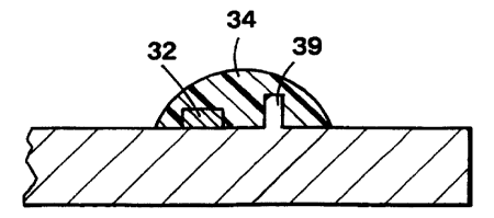
Referring to Figure 2-4b, the three-dimensional
formation may be embodied as a raised member 39 on
substrate 30 adjacent to LED 32. The package of hardened
encapsulating material 34 forms a mechanical bond with
substrate 30 and raised member 39 in a manner similar to
that described above when hole 31 is provided.
Referring to Figure 2-5, a section view of mold
100, substrate 30 is positioned on top of base plate 40
CA 02274577 1999-06-09
WO 98/25749 PCT/US97122593
- 15 -
within closed mold 100. Gate plate 20 includes gate 21
and cavity 24. Gate 21 communicates with inlet 11
through distribution runner 25. Cavity 24 communicates
with gate 21. Gate plate 20 is positioned so that
ejection holes 26 are located over ejection pins 41 of
base plate 40. Ejection pins 41 are spring-loaded and,
when extended, extend completely through ejection holes
26 and above gate plate 20. When mold 100 is closed,
ejection pins 41 are compressed downward by the weight of
top plate 10.
Referring to Figure 2-6, as shown, gate 21 is
conical in shape and includes an input 22 and an output
23. Input 22 communicates with inlet 11 of top plate 10
through distribution runner 25. Output 23 communicates
with cavity 24. The cross-sectional area of gate 21
decreases from input 22 to output 23. This reduction of
cross-sectional area results in a region of reduced
strength in the hardened encapsulating material near
output 23. In one embodiment, gate 21 has a
substantially round input 22 with a cross-sectional area
of about 0.000615 square inches and a substantially round
output 23 with a cross-sectional area of about 0.000113
square inches, and is about 0.065 inches long, which
provides the intended region of reduced strength near
output 23 in a thermoplastic encapsulating material such
as LexanT"", a polycarbonate available from General
Electric. Alternatively stated, a gate having side walls
28 that are inclined about 15 degrees over their length
from the inlet to the outlet will provide the desired
shape.
Referring again to Figure 2-5, in operation, mold
100 is closed with substrate 30 positioned inside.
Substrate 30 rests on rigid base plate 40. An
encapsulating material {not shown) is injected into mold
100 through inlet 11 in top plate 10. The encapsulating
CA 02274577 1999-06-09
WO 98/25749 PCT/U597/22593
- I6 -
material may be any thermoplastic resin, such as, for
example, polycarbonate or acrylic. Use of thermoplastic
resins is advantageous because they harden by loss of
heat typically in a few seconds and thus provide for very
short cycle times. Further, excess thermoplastic
material not forming part of the encapsulating package
may be recycled and reused simply by reheating. In
addition, the shrinking of a thermoplastic as it cools
allows for the formation of a strong mechanical bond to
the substrate as discussed above.
When injection molding a package particularly
around a light emitting device, such as a LED, or light
receiving device) such as a photodiode, the encapsulating
material must be sufficiently transparent. A variety of
transparent and translucent plastic resins are available
that meet the required characteristics. A polycarbonate
resin, such as LexanT"', for example, available from
General Electric, is suitable for encapsulating an LED.
Referring again to Figures 2-5 and 2-6, the
injected encapsulating material passes through inlet 11
into distribution runner 25 and from there through input
22 into gate 21 and through output 23 to cavity 24.
Enough encapsulating material is injected to completely
fill cavity 24, gate 21, distribution runner 25 and part
of inlet 11. Each cavity 24 is formed so that the
encapsulating material flows in and around a
corresponding hole 31 in substrate 30. The high
viscosity of the thermoplastic encapsulating material
prevents it from leaking beyond the boundaries formed by
cavity 24 and hole 31. In addition, the pressure of the
mold is sufficient to form a seal between the substrate
30 and base plate 40 and cavity 24 and substrate 30 to
contain the injected thermoplastic. Once fully
injected, the encapsulating material is allowed to
harden. This hardening may be accomplished through loss
CA 02274577 1999-06-09
WO 98125749 PCT/US97/22593
- 17 -
of heat in a matter of seconds when the appropriate
thermoplastic resin is chosen as the encapsulating
material.
Referring to Figure 2-7, the top portion of gate
plate 20 includes gates 21, distribution runner 25 and
ejection holes 26. Referring to Figure 2-8) the bottom
portion of gate plate 20 further includes cavities 24 and
locator holes 27. When positioned in mold 100, locator
holes 27 fit over locator pins 42 in base plate 40.
l0 To encapsulate a small device, one requires a
small cavity 24 and small gate 21. With very small
gates, the gate tends to clog or freeze off, preventing
the flow of encapsulating material. This tendency may be
overcome by making the length of gate 21 short and
locating gate 21 close to cavity 24. To facilitate a
short gate 21, gate plate 20 is of thin construction
relative to the overall height of mold 100. It has been
found that a gate plate 20 of about 0.25 inches in
thickness is suitable for use in a method and apparatus
for injection molding a package around an LED. The
addition of runner 25 in the top of gate plate 20 allows
the length of gate 21 to be further reduced. A gate 21
of about 0.065 inches in length from input to output is
well suited for use in encapsulating LEDs. The shorter
gate provides an additional advantage in that the
thermoplastic material may be maintained at a higher
temperature because the short distance from the heating
elements to the cavity prevents substantial cooling. The
higher temperature results in a thermoplastic with a
lower viscosity which improves the injection process
further and results in less damage to delicate devices
and connections.
The small size of gates 21 and cavities 24 and
their proximity to one another also results in a gate
plate that may wear significantly with repeated use,
CA 02274577 1999-06-09
WO 98125749 PCT/US97122593
- 18 -
eventually allowing leakage between the cavity segments.
Use of a thin gate plate 20 that is separate from the
larger top and bottom plates {10 and 40) of mold 100,
however, allows design of a replaceable gate plate which
may be constructed of relatively inexpensive material
relative to the other components of mold 100.
Referring to Figure 2-9, the shape of cavity 24
and gate 21 may be seen in detail. The shape of cavity
24 is chosen to provide a package of hardened
encapsulating material {34 of Figure 2-3) that completely
encloses LED 32 and fills hole 31. Cavity 24 may,
however, be of any shape, and the shape will depend on
the particular device being enclosed. The cavity may,
for example, be substantially rectangular, or round, or
trapezoidal at its base and taper to the output of its
corresponding gate which itself may be, for example,
round, square, triangular, rectangular, or oval. As
shown, gate 21 is conical in shape with a substantially
round input and substantially round output. However,
gate 21 also may be of any shape and may, for example, be
pyramid-shaped, substantially rectangular in cross-
section, or the like.
A further advantage to the use of gate plate 20 is
the versatile placement of gates 21 and cavities 24.
Because they are formed entirely in gate plate 20, gates
21 and cavities 24 may be located anywhere in gate plate
20. Further, all of the gates may be fed from the same
distribution runner which may be located in gate plate 20
or in top plate 10. Accordingly, the devices to be
encapsulated may be located in any configuration on
substrate 30. The need for a lead frame to hold the
devices is thus eliminated. These devices may even be
located near or around other devices that have previously
been encapsulated or mounted to substrate 30 by providing
cut outs in gate plate 20 to accommodate these other
CA 02274577 1999-06-09
WO 98125749 PCT/US97122593
- 19 -
devices. The small size of gate 21 and cavity 24 and
versatility of replaceable gate plate 20, allow for very
accurate placement of an encapsulating material and thus
allow far a large number of small devices to be
individually encapsulated in close proximity to one
another and in any location or arrangement on a
substrate.
Referring to Figure 2-10, once the encapsulating
material has hardened, top plate 10 is removed from gate
plate 20. Ejection pins 41 are automatically released by
the removal of the weight of top plate 10 and spring
upward, ejecting the excess hardened encapsulating
material 50 off of gate plate 20. The excess hardened
encapsulating material 50 breaks off near output 23
(Figure 2-6) under the pressure from ejection pins 41.
Thus, substantially all of the excess hardened
encapsulating material outside of cavity 24 is
automatically removed when the mold is opened,
eliminating the need for any additional milling or
polishing step. Excess hardened encapsulating material
50 may be recycled by being reheated and then used to
encapsulate additional devices.
Referring to Figure 2-11, cavity 24 encloses LED
32 and its adjacent hole 31. As shown in Figure 2-11 and
discussed above, after injection, the encapsulating
material fills cavity 24 and hole 31 and fully encloses
LED 32. Also as shown in Figure 2-11 and discussed
above, the hardened encapsulating material breaks off
near output 23 of gate 21 when mold 100 is opened.
Referring to Figure 2-12, mold 100 is further
opened by removing gate plate 20 and substrate 30 is
thereafter removed from mold 100. The devices on
substrate 30 are encapsulated by the hardened
encapsulating material as show in Figure 2-3 and
discussed above.
CA 02274577 1999-06-09
WO 98/25749 PCT/US97I22593
- 20 -
Referring to Figure 3) mold 100 is contained
within injection molding apparatus 200. Injection
molding apparatus 200 is of a type well-known in the art
which is commercially available, for example, from
Arburg, Inc. of Newington, Connecticut. Injection
molding apparatus 200 generally includes hopper 201)
screw 203, barrel 205, nozzle 207 and clamp 209. A mold,
such as for example, mold 100, is secured under pressure
in clamp 209. In normal operation, the raw encapsulating
material (not shown) to be injected is placed in hopper
201 and a portion of this material enters barrel 205.
Screw 203 rotates inside barrel 205. This rotation works
the encapsulating material into the proper molten state
through friction and the application of heat. The
rotation of screw 203 also works the encapsulating
material through barrel 205 toward nozzle 207. Once the
encapsulating material is in the proper state, screw 203
is translated along barrel 205 applying pressure to the
encapsulating material and forcing it through nozzle 207
into mold 100.
The present invention has been described in terms
of specific embodiments. The invention, however, is not
limited to these specific embodiments. Rather, the scope
of the invention is defined by the following claims, and
other embodiments are within the scope of the claims.