Note: Descriptions are shown in the official language in which they were submitted.
CA 02274637 1999-06-08
WO 99/20004 PCT/US98/17743 -
- 1 -
Description
SIGNAL PROCESSING METHOD AND DEVICE
BACKGROUND OF THE INVENTION
The invention relates to digital signal pro-
cessing and specifically to controlling the level of a
pulse density modulation (PDM) signal generated by a
sigma-delta modulator.
BACKGROUND OF THE INVENTION
The basic operations of signal processing,
multiplication and addition, can be implemented in a
known manner by analog signal processing blocks, or an
analog signal can be converted into a digital one by
using an A/D converter and the desired signal processing
operations can be performed digitally. The results can
be reconverted into analog signals by using a D/A con-
verter. The A/D and D/A conversions are performed at
predetermined sample frequency and at a predetermined
resolution.
A/D and D/A convertors based on sigma-delta
modulators have become very common recently. In a sigma-
delta A/D convertor, a conversion of an analog signal
into a baseband digital signal occurs at two stages. At
the first stage, an input signal is converted by a sigma-
delta modulator into an oversampled single-bit or
multibit signal. At the second stage, this oversampled
single-bit or multibit signal is decimated to the
baseband by using digital filtering. Sigma-delta tech-
nique and converters are described for instance in the
following articles:
[1] "An Overview of Sigma-Delta Converters",
P.M. Aziz et al, IEEE Signal Processing Magazine, January
1996, pages 61 to 84.
[2] "Oversampling Delta-sigma Data Converters:
Theory, Design and Simulation", J.C. Candy et al, IEEE
Press NJ 1992, pages 1 to 25.
CA 02274637 1999-06-08
WO 99/20004 PCT/US98/17743
- 2 -
I3] ~~Design Methodology for Sigma-Delta
Modulation~~. B.P. Agrawal et al, IEEE Transactions on
Communications, Vol. COM-31, March 1983, pages 360 to
370.
An oversampled output signal of a sigma-delta
modulator is a pulse density modulated (PDM) representa-
tion of an input signal. In sigma-delta A/D converters,
the modulator converts an analog signal into a pulse
density modulated (PDM) format. The PDM signal consists
of an oversampled single-bit or multibit (e.g. 2 to 4
bits) signal. The relative pulse density of the PDM
signal determine represents the amplitude of the input
signal. In a frequency domain, the baseband part of the
spectrum of the PDM signal is the useful signal band, and
at higher frequencies of the spectrum, there is
quantization noise produced by a noise processing func-
tion of the sigma-delta modulator. It has thus been
possible to change the resolution at signal frequencies
for over-sampling rate. As known, the noise processing
performance of the sigma-delta modulator depends on the
order of the modulator, and higher-order modulators
remove quantization noise more efficiently from the
signal band. By increasing the oversample ratio, the
signal band can also be made narrower, in proportion, and
the amount of the noise falling on the signal band
smaller. Moreover, the amount of noise in the signal
band in a sigma-delta modulator can be controlled by the
transfer function of the modulator, e.g. by inserting
zeroes at suitable frequencies in the transfer function
of the modulator.
Solutions for implementing a limited number of
signal processing operations by using PDM signals have
been presented in the literature lately. The known
advantages of digital signal processing are then
achieved, such as accuracy, repeatability, unsensitivity
to interference, and so on. When a signal is processed
directly in an oversampled PDM format, it needs not be
converted into a pulse code modulated (PCM) signal at the
CA 02274637 1999-06-08
WO 99/20004 PCT/US98/17743
- 3 -
Nyquist frequency for signal processing. Decimation and
interpolation filters generating a baseband PCM signal
from a PDM signal can then be omitted in signal process-
ing points. This is a remarkable advantage, because a
circuit implementation of a sigma-delta modulator gener-
ating the PDM signal is usually small in size and simple,
while the decimation and interpolation filter often is a
big and complex circuit structure requiring much circuit
surface in an integrated circuit implementation and
therefore causing additional costs. For instance, the
article [4], ~~Design and Analysis of Delta-Sigma Based
IIR Filters~~, D.A. John et al, IEEE Transactions on
Circuits and Systems-II: Analog and Digital Signal
Processing. Vol. 40, NO. 4, pages 233 to 240, describes
an A/D converter having many inputs, each input being
filtered separately and summed together before a common
decimation filter. An audio mixing board, for instance,
can be implemented in this way.
An important form of signal processing is
control of signal level: amplification and/or attenua-
tion. This property is very usable especially for audio
applications, such as the above-mentioned audio mixing
board. Accordingly, it would be preferable, if a PDM
signal level also could be controlled. Figure 1 of the
above article [4] shows a sigma-delta attenuator, in
which an oversampled 1-bit signal (PDM) is multiplied by
a multibit coefficient al and the resulting multibit
signal is applied to a digital sigma-delta modulator
outputting a 1-bit PDM signal. The multiplier of the 1-
bit PDM signal is implemented as a 2-input multiplexor
(selector) selecting al or -al as an output according to
the state of the incoming PDM signal. The article also
describes a digital sigma-delta filter suitable for this
purpose. The attenuator is possible to implement when
said multibit coefficient is lower than one. The feed-
back value of the sigma-delta modulator being b and said
coefficient being a, an attenuation ratio a/b is ob-
tained.
CA 02274637 1999-06-08
WO 99/20004 PCT/US98/17743
- 4 -
A problem with this known solution is that only
an attenuation of a PDM signal has been possible, and
therefore, it has been necessary to perform all multipli-
cations by coefficients lower than one. An amplification
of a PDM signal has not been considered possible, because
the input value of the modulator cannot exceed or even
come near the feedback value of the modulator due to the
structure of the sigma-delta modulator. The sigma-delta
modulator is a conditionally stable structure and the
output signals of integrators escape upon the input
exceeding a predetermined value. In an analog sigma-
delta modulator, the input value is allowed to be nor-
mally, depending on the order and the structure of the
modulator, approximately 0.3 to 0.7 times the feedback
value, cf. article [3]. An amplification of the PDM
signal in such a circuit would require an ingoing signal
to be multiplied by a number higher than the feedback
value. Even if the input level of an A/D modulator were
very low and it could, in principle, be amplified quite
much by setting the input signal values (a) higher than
the feedback value (b), the resulting PDM signal would
have only +1 and -1 values (single-bit case). By multi-
plying, the modulator would momentarily obtain too high
values. The density and energy of the PDM signal would
still be low on an average, but instantaneous values
would make the modulator quickly unstable.
BRIEF DESCRIPTION OF THE INVENTION
An object of the invention is a signal process-
ing method and device, enabling also a relative amplifi-
cation of a PDM signal, without the noise level increas-
ing remarkably.
The objects of the invention are achieved by a
signal processing method comprising the steps of generat-
ing an N-bit pulse density modulated signal by a first
sigma-delta modulator; where N=1, 2, ...; controlling the
level of the pulse density modulated signal a) by multi-
plying the N-bit pulse density modulated signal by a
CA 02274637 1999-06-08
WO 99/20004 PCT/US98/17743
- 5 -
multibit multiplier, the output of which is an M-bit
signal, where M>N, b) by converting the M-bit signal into
an N-but pulse density modulated signal by a digital
sigma-delta modulator. The method is according to the
invention characterized in that the M-bit signal is
converted into the N-bit pulse density modulated signal
by the digital sigma-delta modulator having a better
signal-to-noise ratio performance than said first sigma-
delta modulator.
Another object of the invention is a signal
processing system comprising a first sigma-delta modula-
for generating an N-bit pulse density modulated signal,
where N=1, 2, ...; means for controlling the level of the
pulse density modulated signal, the means comprising a) a
multibit multiplier, the input of which is the N-bit
pulse density modulated signal and the output an M-bit
signal, where M>N, b) a digital sigma-delta modulator
converting the M-bit signal into the N-bit pulse density
modulated signal. The system is according to the inven-
tion characterized in that said digital sigma-delta
modulator has a better signal-to-noise ratio performance
than said first sigma-delta modulator.
A single-bit pulse density modulated PDM signal
is generated by the first sigma-delta modulator being an
analog modulator, for instance. The level control is
performed by multiplying the single-bit PDM signal by a
multibit coefficient, so that a multibit stream of
numbers is obtained. The number stream is reconverted
into a single-bit PDM signal by a second sigma-delta
modulator, preferably being a digital modulator.
In accordance with the basic idea of the
invention, the signal-to-noise ratio performance of said
second sigma-delta modulator, by which the multibit
stream of numbers is reconverted into a PDM signal, is
better than that of said first sigma-delta modulator.
Accordingly, the most significant factor of the total
signal-to-noise ratio (SNR) is the noise level of the
first sigma-delta modulator, by which the PDM signal
CA 02274637 1999-06-08
WO 99/20004 PCT/US98/17743
- 6 -
originally was generated. In said subsequent second
sigma-delta modulator, the PDM signal can be attenuated
within a range which is equal to the difference between
the SNR performances of the modulators, without any
decrease in the total signal-to-noise ratio. For in-
stance, if the SNR of the first sigma-delta modulator is
90 dB at maximum excitation and the SNR of the second
sigma-delta modulator is 110 dB, the PDM signal can be
attenuated in the second modulator by nearly 20 dB
without any decrease in the signal-to-noise ratio. This
is possible, because, in the latter modulator, besides
the signal, naturally also the noise of the first modula-
tor on the signal band is attenuated and approaches the
noise floor set by the second modulator structure.
The PDM signal has thus been scaled to a
slightly lower level without any decrease in the perfor-
mance. Though the second sigma-delta modulator also
attenuates the signal, the attenuation may be less than
said difference between the performances (20 dB in the
above example), whereby a relative amplification is
achieved. When the PDM signal is attenuated less than
said difference between the SNR performances of the two
modulators, the same total signal-to-noise ratio is
obtained as by the preceding analog modulator. In the
example case, the nominal level of the signal can be
fixed to a point where the first modulator gives an
unattenuated signal and the second modulator attenuates
the signal by 20 dB. The second-order attenuation may be
C. In the example case, the total signal-to-noise ratio
will then be 90 dB, the signal being between +20 - 0 dB
and 90 + 20 - (c), c being between 20 and 110 dB, and the
attenuation of the system thus between 0 and 90 dB.
BRIEF DESCRIPTION OF THE DRAWINGS
The invention will now be described in more
detail by way of preferred embodiments, with reference to
the attached drawings, in which
CA 02274637 1999-06-08
WO 99/20004 PCT/US98/17743
Figure 1 is a block diagram illustrating a PDM
level controller according to the invention, connected
after an analog sigma-delta A/D modulator;
Figure 2 is a graph showing noise and signal
levels of an analog sigma-delta modulator and a digital
sigma-delta modulator and a controlling area at disposal
as a function of frequency;
Figure 3 is a block diagram showing a multi-
channel PDM level controller.
DETAILED DESCRIPTION OF THE INVENTION
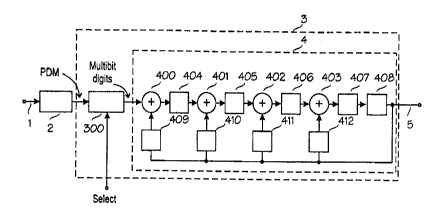
With reference to Figure 1, an analog sigma-
delta modulator 2 performs an A/D conversion of an analog
input signal at an input 1 into a 1-bit pulse density
modulated (PDM) format. The modulator 2 may be, for
instance, any sigma-delta A/D modulator structure de-
scribed in the article [1]. Let us assume that the
modulator 2 is a third-order sigma-delta modulator having
a signal-to-noise ratio of about 100dB. A single-bit PDM
signal, which may obtain the values +1 and -1, is applied
to a PDM level controller 3.
The PDM level controller 3 according to a
preferred embodiment of the invention comprises a digital
modulator 4 and a preceding multiplier 300. Level
control is performed by multiplying the single-bit pulse
density modulated (PDM) signal by a multibit coefficient
a in the multiplier 300 in order to obtain a multibit
number stream, which is reconverted into a single-bit PDM
signal by means of a digital sigma-delta modulator 4.
In the case of single-bit PDM signal, the
multiplier 300 can be implemented by a simple multiplexor
or selector, generating an output +a or -a depending on
whether the input value is +1 or -1. The output of the
multiplier 300 is thus a multibit number stream consist-
ing of the numbers +a and -a. The multiplier 300 may
have a structure similar to the one disclosed in the
article [4]. The multiplier may have one fixed coeffi-
cient or the value of the coefficient may be adjustable.
CA 02274637 1999-06-08
WO 99/20004 PCT/US98/17743
- g _
In the preferred embodiment of the invention shown in
Figure l, a selection signal SELECT may choose one of
several coefficients al...an, and accordingly, a desired
attenuation or amplification can be set. The coeffi-
cients may be in accordance with Table 1, for instance.
The Table indicates 32 values of the coefficient a,
giving a level control range of +12 dB ...-34,5 dB by 1.5
dB steps.
Table 1
Coefficient Amplification
a (dB)
872 +12.0
734 10.5
617 9.0
519 7,5
437 6.0
368 4.5
309 3.0
260 1.5
219 0
184 -1.5
155 -3.0
130 -4.5
110 -6.0
92 -7.5
78 -9.0
65 -10.5
55 -12.0
46 -13.5
39 , -15.0
33 -16.5
28 -18.0
23 -19.5 _
20 -21.0
CA 02274637 1999-06-08
WO 99/20004 PCT/US98/17743
_ g _
16 -22.5
14 -24.0
12 -25.5
10 -27.0
8 -28.5
7 -30.0
6 -31.5
5 -33.0
4 -34.5
The digital modulator 4 is a fourth-order
modulator, comprising summers 400 to 403, integrators 404
to 407, a quantizer 408 and feedbacks 409 to 412, having
the feedback coefficients rl to r4, respectively. It is
to be noted that a detailed implementation and structure
of the modulator 4 is of no significance for the inven-
tion. Only the fact that the performance of the modula-
tor 4 is better than that of the modulator 2 is of
significance for the invention, as will be described
below. The input of the modulator 4 is said number
stream consisting of the numbers +a and -a. The output 5
of the modulator 4 is a 1-bit oversampled PDM signal.
The level of the PDM signal is controlled in the level
controller 3 at the ratio a/rl. On account of the
unstable nature of the sigma-delta modulator, the input
value of the modulator 4 cannot approach the internal
reference voltage value of the modulator, which means
that the coefficient a shall be lower than the feedback
coefficient rl. Therefore, the PDM signal can only be
attenuated in the multiplier 300.
At the system level, i.e. between the input 1
and the output 5, amplification can be provided, however,
when the performance of the digital sigma-delta modulator
is higher than that of the modulator 2, as to the noise
processing performance. The noise processing performance
of the modulator 4 may be higher thanks to higher order,
multibit quantization and feedback or higher oversampling
CA 02274637 1999-06-08
WO 99/20004 PCT/US98/17743
- 10 -
ratio, or some combination of these, for instance. In
the embodiment of Figure 1, the modulator 4 is a fourth-
order modulator, while the modulator 2 is a third-order
modulator. When a higher-order modulator (or a modulator
having otherwise a better noise processing performance)
follows a lower-order modulator on the processing path of
the PDM signal, the noise level of the lower-level
modulator is most decisive for the total signal-to-noise
ratio (SNR) of the system. In the case of Figure 1, the
signal-to-noise ratio at the output 5 is thus primarily
determined on the basis of the signal-to-noise ratio of
the modulator 2. The performance of the modulator 4
shall be at least a desired need of amplification and
preferably also a suitable stability margin better than
the signal-to-noise ratio of the modulator 2 and the
incoming PDM signal. Because the signal-to-noise ratio
of the modulator 4 of the level controller 3 is consider-
ably better than that of the incoming PDM signal, the
level controller may lower the level of the whole PDM
signal without practically any decrease in the signal-to-
noise ratio at all. This is possible, because in addi-
tion to the noise of a payload signal, also the noise of
the PDM signal is attenuated. The signal has thus been
scaled to a slightly lower level without any decrease in
the performance. Though the PDM signal is attenuated
also in the modulator 4, it is possible to attenuate the
signal in the level controller 3 less than said differ-
ence between the performances of the modulators 2 and 4
and to achieve a relative amplification.
Let us examine the operation of the level
controller according to the invention by way of example
with reference to the graph of Figure 3. Assuming that
the analog modulator 2 is a third-order modulator, the
signal-to-noise ratio of which is about 100 dB. The
modulator 4 is a fourth-order digital modulator, the
signal-to-noise ratio of which is about 120 dB, i.e.
about 20 dB better than that of the modulator 2. The
desired control range is +12 dB...-34,5 dB by 1.5 dB
CA 02274637 1999-06-08
WO 99/20004 PCT/US98/17743
- 11 -
steps. To ensure the stability of the modulator 4, the
ratio a/rl is 0.5, i.e. -6 dB. The value of the refer-
ence rl can be calculated as a function of the maximum
attenuation (-34.5 dB) and the required accuracy (<0.3
dB). Accordingly, the reference value is assumed to be
1744. The amplification +12 dB is now corresponded to by
multiplying the incoming PDM signal by 872 and the
maximum attenuation is corresponded to by multiplying the
PDM signal by 4. In the above Table 1, all different
values of the coefficient a are listed, and so are the
corresponding amplifications, when the value of the
reference rl is the constant 1744. The different between
the performances of the modulators 2 and 4 being 20 dB
and the stability margin being set to 6 dB, the range of
amplification at disposal is about 14 dB.
In the present example, the signal-to-noise
ratio remains approximately the same in the range +12...
-1.5 dB as it is after the modulator 2. At higher
attenuation, the noise of the very input signal is
attenuated below a noise floor 22 of the modulator 4, the
attenuated payload signal 25 and the noise floor 22
determining the signal-to-noise ratio at the output 5.
The invention is described above in conjunction
with a 1-bit PDM signal. The invention can, however, be
applied directly to a multibit, e.g. 2-bit to 4-bit, PDM
signal as well.
The preferred embodiment of the invention
described in Figure 1 shows the analog modulator 2, the
multiplier 300 and the digital modulator 4 sequentially
connected. In practice, these units may be located apart
from each other in the signal processing system in such a
way that there are other signal processing stages between
them. An example of such a signal processing system is
shown in Figure 3.
Figure 3 shows three analog input signals 31,
32 and 33, which are applied to respective analog sigma-
delta modulators 34, 35 and 36. The modulators 34, 35
and 36 generate PDM signals 37, 38 and 39, respectively,
CA 02274637 1999-06-08
WO 99/20004 PCT/US98/17743
- 12 -
which are applied to multipliers 40, 41 and 42, respec-
tively. The multipliers 40, 41 and 42 generate multibit
number streams 43, 44 and 45, respectively, which are
summed in a summer 46 to a multibit number stream 47.
The signal 47 is converted into a PDM signal 49 by a
digital sigma-delta modulator. The modulators 34 to 36
may have a structure similar to that of the modulator 2
in Figure 1. The structure of the multipliers 40 to 42
may be similar to that of the multiplier 300 in Figure 1.
The modulator 48 may have a structure similar to that of
the modulator 4 in Figure 1. An application of the
signal processing apparatus of the type shown in Figure 3
is an audio mixing board.
The invention can be applied to the level
control of a PDM signal in all sigma-delta structures.
Typical objects of application are, besides audio appli-
cations, also IIR and FIR filter structures.
It is obvious to one skilled in the art that,
with the technique developing, the basic idea of the
invention can be implemented in many different ways.
Accordingly, the invention and its embodiments are not
restricted to the above examples, but they may vary
within the scope of the claims.