Note: Descriptions are shown in the official language in which they were submitted.
CA 02274785 2003-04-08
A CHIP MODULE AND PROCESS FOR THE PRODUCTION (HEREOF
The present invention relates~to a chip module with a
substrate and at least one chip arranged on the substrate,
a wherein the chip is contacted via terminal surfaces arranged
on its front side onto connecting leads of the substrate
provided with a conductor path structure and the chip has a
thickness which is reduced compared to its original
thickness. The present invention further relates to a
process for the production of a chip module with a substrate
and at least ane chip arranged on the substrate, wherein a
handling unit with a chip and a substrate is formed by
contacting the chip or chips onto the substrate provided
with a conductor path structure in such mannex that the chip
or chips is/are~contacted by its/their terminal surfaces
onto connecting leads of the substrate, and wherein the
processing of the chip or chips is effected by a material
removal process on its or their rear side, the substrate
providing for the handling and stabilization of the chip or
chips during the processing.
Chip modules comprising a chip arranged on a substrate are
basically used in all cases in which simplified electric
contacting of the chip is to be facilitated by means of
substrate connecting leads which are substantially larger
than the chip terminal surfaces. Thus such chip modules are
used, for example, in chip cards and via the exposed
substrate connecting leads extending over the card surface
permit "external contacting" of the chip accommodated inside
the chip card by the arrangement on the rear side of the
substrate. Such chip modules are also used to construct so-
called contactless chip cards in the case of which the
substrate connecting leads provide for simplified contacting
with an antenna coil arranged inside the card body.
Naturally such chip modules can also be used, for exampJ.e,
CA 02274785 2003-04-08
1a
. to construct a so-called "combi-card" in the case of which
external contacting for contact access to the card chip as
well as internal. contacting for contactless access to the
chip via the antenna coil are faciJ.ztated by means of the
substrate.
The combination of a chip with the substrate to form the
chip module results i.n a comn.nsitP .strmr_to.rP,, the thickness
of which is relatively great compared to the thickness of
the chip and the thickness of the substrate and which must
be accommodated in a card body with defined outer
dimensions. To ensure that the accommodation o~ a chip
module in a card body imposes the Least possible
restrictions upon the possibilities of further component
installations in the card body, it thus proves essential
CA 02274785 1999-06-09
2 lv~';::..
for the chip module to be designed to be as thin as
possible.
A disadvantage of the known, relatively thick chip modules
is that simply by virtue of their relative thickness, they
have greater bending resistance compared to the flexible
card body and therefore when the card body is subjected to
bending stress as frequently occurs in everyday use, in
particular when the substrate is arranged in the card
surface as in the case of a contact card, the connection
between chip module and card body can be stressed to a high
level, leading to the detachment of the chip module from
the card body.
US-A-5,155,068 has disclosed a chip module and process for
the production of a chip module wherein the connection
between chip and substrate is established in two
consecutive process steps in which firstly the electric
contacting of the bonding pads of the chip to terminal
surfaces of the substrate is performed and then the
mechanical connection between the chip and the chip
substrate is effected by embedding the entire chip into a
synthetic resin compound surrounding the chip. As a result
of the embedding of the chip into the synthetic resin
compound surrounding the chip, during the following
abrasive processing of the rear side of the chip it is
necessary to abrasively remove the material surrounding the
chip in addition to the chip material.
JP-A-63 147 352, referred to in "Patent Abstracts of
Japan", also discloses a process for the production of a
chip module wherein the connection between chip and chip
substrate is established in two process steps and wherein
the chip is embedded in a synthetic resin compound for
mechanical connection to the chip substrate.
CA 02274785 2003-04-08
3
Ep-A-0 2~~ 853 has disclosed a process wherein a plurality
of chip modules are produced continuously using a film
carrier.
The object of the present invention is to propose a chip
module and a process for the production of a chap module
facilitating the simplified establishment of a connection
between a chzp and a chip substrate and more effective
processing of the chip to reduce the chip thickness.
This object is achieved by means of a chip module comprising
a substrate and at least one chip arranged on ~he substrate,
wherein the chip is contacted via terminal surfaces arranged
on its front side onto connecting leads of the substrate
provided with a conductor path structure and the chip has a
thickness which is reduced compared to its original
thickness, characterised in that in order to obtain an
interlocking contacting with bonding pads formed on the
terminal surfaces, the chip projects with the bonding pads
into recesses of the substrate, a base of the recesses being
formed by the connecting leads of the conductor path
structure and the bonding pads of the chip are embedded in a
connecting material which is arranged in the recesses of the
substrate, the connecting material serving both for the
electrical contacting of the chip and for the mechanical
connection of the chip to the substrate.
The chip module according to the invention utilizes the fact
that the electric circuit planes in the silicon body of the
chip axe adjacent to the front- or contact sidE of the chip
provided with the terminal surfaces, and the region of the
silicon body adjoining the surface of the rear side is tree
of electrzc circuzt planes. rt is thus possible, without
CA 02274785 2003-04-08
3a
impairing the function of the chip, to remove the surface of
the chip from the rear side until a minimum thickness of the
chip body ensuring satisfactory chip functioning is
obtained, and in this way to make the chip substantially
thinner.
The reduction in thickness of the chip not only facilitates
a corresponding reduction in the overall thickness of the
chip module but also enables the bending behavior of the
chip module to be influenced. As a result of the reduction
in the chip thickness, the bending behavior of the chip is
adapted to the bending behavior o~ the substrate, thus
leading to an overall mare readily bending, more flexible
chip module, the bending behavior o~ which resembles that of
the card body.
In the chip module according to the invention, in order to
achieve an interlocking contacting with bonding pads formed
I
CA 02274785 1999-06-09
on the terminal surfaces, the chip projects into recesses
of the substrate whose base is formed by the conductor path
structure. The engagement of the bonding pads in the
recesses of the substrate leads to a connection between
chip and substrate with particularly good shearing
strength. Furthermore, due to this "sunken" arrangement of
the bonding pads in the substrate, a particularly planar
design of the chip module is achieved simply by virtue of
its configuration.
Here the bonding pads of the chip are embedded in an
electrically conductive connecting material which is
arranged in the recesses of the substrate and provides both
for the electrical contacting of the chip and for the
mechanical connection of the chip to the substrate. By
means of this embedding of the bonding pads in the
connecting material it is also easily possible to
compensate for any tolerances occurring in the difference
between the height of the bonding pads and the depth of the
recesses through the connecting material and, while
retaining a reliable, electrically conductive connection
between the bonding pads of the chip and the connecting
leads of the substrate, to provide the flattest possible
overall arrangement of chip and substrate wherein the
surface of the chip and the surface of the substrate can
adjoin one another directly, thus without a gap. In the
production of the chip module according to the invention it
is thus also possible to omit the application of an
underfiller known in the context of underfiller technology.
The mechanically stabilising effect of the underfiller
which improves the shearing strength of the chip module can
also be dispensed with since a particularly stable,
mechanical'load-bearing connection is provided by the
"embedding" of the bonding pads and the associated covering
of the bonding pads with the connecting material on all
sides, at least in partial regions of the contact
metallizations.
CA 02274785 2003-04-08
The bonding pads can be formed from any electrically
conductive material, such as for example an electrically
conductive adhesive or a contact metallization made of
solder material ox the like.
The above described form of interlocking contacting between .
a chip and a substrate also has substantial advantages
regardless of whether the contacted chip is a chip reduced
in thickness by the removal of mater;~al or is a conventional
chip, especially when a mechanically stable chip module is
to be constructed.
To further increase the mechanical stability of the .
connection provided between chip and substrate in the chip
module, at least one further projection which is
electrically independent of the chip structure can be
provided on the chip surface in addition to the bonding pads
electrically conductively connected to the chip structure.
said projection engaging into a f'~xing recess of the
substrate. This projection, which can be designed and
produced to be identical to the bonding pads forming
electric terminals, provides a "contact dummy" which has
merely a mechanically stabilizing function.
If desired, further mechanical stabilization or seaJ.ing can
be provided by a peripheral or planar application of
adhesive.
A particularly advantageous use of the chip module is in a
chip card.
According to the invention, there is provided a process for
the production of a chip module comprising a substrate and
~t laast nno chip arrar~rJ,ed nr~ ~~Q._e.We.t~at~,....,he~eir_._~.._
.._____.____ _
handling unit consisting of at least one chip and a
CA 02274785 2003-04-08
5a
substrate is formed by contacting the chip onto the
substrate provided with a conductor path structure in such
thereof onto connecting leads of the substrate, and wherein
the processing of the chip is effected by a maternal removal
process on a rear side thereof, the substrate providing for
the handling and stabilisation of the chip during the
processing, characterised in that for the formation of the
handling unit, the chip is contacted onto the substrate such
that bonding pads arranged on the terminal surface of the
chip are inserted into a connecting material arranged in
recesses of the substrate. In this way a connection can be
obtained
CA 02274785 1999-06-09
l,~f.r:
which withstands even the highest levels of shearing
stress, such as occur for example during the grinding
processing of the rear side of the chip, as the connection
established by the embedding of the bonding pads into the
connecting material is additionally secured by the
engagement of the bonding pads into the recesses of the
substrate.
Prior to the contacting of the terminal surfaces, selective
cleaning can take place of the chip terminal surfaces t.o be
contacted and/or of the substrate contact surfaces or the
bonding pads or connecting material surfaces optionally
applied thereto.
The processing of the chip or chips can be performed using
a grinding or lapping process. Another possible method of
processing the chips to form a chip module of reduced
thickness consists of performing a chemical etching process
on the rear side of the chip.
The connecting material required to form the connection can
differ in type and form. Thus, for example, prior to the
insertion of the bonding pads into the recesses, the
connecting material can be introduced into the recesses by
planar application to the surface of the insulating.layer
and subsequent stripping off of the surface.
It.is also possible to introduce the connecting material
into the recesses in a liquid state, before or after the
insertion of the bonding pads into the recesses, in a
dosing process.
Another possible method of applying the connecting material
consists of introducing the connecting material into the
recesses in lump form, for example lead/tin solder spheres,
prior to the insertion of the bonding pads.
CA 02274785 1999-06-09
7 1~P:::
The substrate used to produce the chip module can also have
been pre-prepared inasmuch as the bonding pads are inserted
into recesses already provided with a coating of connecting
material in the region of the connecting leads. It is thus
possible for the process according to the invention for the
production of a chip module also to be performed on the
basis of substrates appropriately pre-prepared by the
substrate manufacturer, thereby facilitating a particularly
cost-effective implementation of the process.
If the connection between the connecting material and the
bonding pads and between the connecting material and the
connecting leads takes place under the influence of
pressure and heat, a connection between chip and substrate
is ensured in which the adjacent surfaces of chip and
substrate bear against one another whereby, when an
appropriate quantity of connecting material is provided, an
at least partial embedding of the bonding pads into the
connecting material occurs, even in the case of a
connecting material with high boundary surface tension.
The connection between the connecting material and the
bonding pads can be implemented in accordance with the
known flip-chip method in which the bonding pads of the
chip are pressed against the connecting material under
thermal influence. The heating of the connecting material
necessary for the establishment of the connection thus
takes place during the placement.
However, the connection can also be implemented such that
only after the placement does the heating of the connecting
material and the establishment of the connection take place
in a so-called reflow process.
Irrespectively of the time at which the heat is introduced
into the connecting material, it has proved particularly
advantageous for the introduction of the heat into the
CA 02274785 2003-04-08
connecting material to take place via the connecting leads
of the substrate. In this way the chip remains substantially
free of thermal stress during the establishment of the
connection_
It is also advantageous if a function test of the chip is
performed following the processing of the chip. Here the
connecting leads of the substrate form the test contacts.
The implementation of this electric test, generally a
continuity test, facilitates the detection of a chip module
which has been functionally impaired, possibly due to the
processing of the chip or due to the formation of the
connection between chip and substrate.
Also in accordance with the present invention, there is
provided a chip module comprising:
a substrate with connecting leads and recesses;
a chip arranged on said substrate, said chip having
terminal surfaces arranged on a chip front side and
being contacted via said terminal surfaces onto
connecting leads of the substrate provided with a
canductor path structure, said chip having a thickness
which is reduced compared to an initial thickness of a
wafer from which said chip has been formed;
bonding pads formed on said terminal surfaces, said chip
projecting with said bonding pads into said recesses of
the substrate, the base of said recesses being formed
by said connecting leads of said conductor path
structure and said bonding pads being embedded in a
connecting material which is arranged in sand recesses
of said substrate, said connecting material defining an
electrical contact of said chip and providing a
mechanical connection of said chip to said substrate.
CA 02274785 2003-04-08
8a
Further in accordance with the present invention, there is
provided a chip module comprising:
a substrate with connecting leads and recesses;
a chip arranged on said substrate, said chip having
terminal surfaces arranged on a chip front side and
being contacted via said terminal surfaces onto
connecting leads of the substrate provided with a '
conductor path structure;
bonding pads formed on said terminal surfaces, said chip
projecting into said recesses of the substrate whose
base is formed by said connecting leads of said
conductor path structure and said bonding pads being
embedded in a connecting material which is arxanged in
a recesses of said substrate, said connecting material
defining an electrical contact of said chip and
providing a mechanical connection of said chip to said
substrate;
at least one further projection, in addition to the
bonding pads, which are electrically conductively
connected to the conductor path structure and engage
into the recesses, said further projection being
electrically independent of said conductor path
structure and being provided on a front side of said
chip, said projection engaging into a fixing recess of
said substrate.
Still further in accordance with the present invention,
there is provided a chip module comprising:
a substrate defining a plurality of recesses and including
a plurality of connecting leads forming a base of said
plurality of recesses;
a chip including an electrical circuit region and a
plurality of terminal surfaces electrically connected
to said circuit region, said terminal surfaces
including bonding pads, said chip module being arranged
CA 02274785 2003-04-08
8b
on sand _.svhstratP wi.th__said nlural.it~C.nf_bonding .pads
arranged in said plurality of recesses; ,
a connecting material in said plurality of recesses and in
contact with said connecting leads and said bonding
pads, said connecting material forming an electrical
connection between said connecting leads, said bonding
pads and said terminal surfaces, said connECting
material also forming a ntechanicai corineczion neLween
said chip and said substrate.
In the following the chip module according to the invention
will be explained in detail in the form of an exemplary
embodiment and a process for its production, making
reference to the drawings in which:
figure I is a.perspecti~re view of a chip module comprising
a chip and a substrate arranged thereon;
CA 02274785 2003-04-08
9
Figure 2 is an enlarged side view of the chip module
illustrated in Figure 1;
Figure 3 is an enlarged paxt~al view of the chip module
according to Figure 2;
Figure 4 is a view corresponding to Figure 3 directly prior
to the connection of the chzp to the substrate to
form the chip module;
Figure 5 is a schematic diagram of a device for the
continuous production of the chip module shown in
Figure l: ,
Figure 6 is a partial view of a substrate strip with
individual substrates.
Figure 1 illustrates a chip module 10 comprising a chip 11
and a substrate 12 contacted thereto. On the upper side of
the chip module, facing away from the chip 11, an insulating
layer is provided in the form of a carrier layer 13. On the
upper side of the carrier layer 13, the substrate 12
comprises connecting leads 14, 15 which in the example shown
here are provided in duplicate, The connecting leads 14 and
15 extend upon and substantially longitudinally over the
carrier layer 13.
In the exemplary embodiment shown in Figure 1, the chip 11
comprises two xaised contact metallizations 16, 17, referred.
to in the literature of the art as "bumps", which penetrate
through and project from a passivation layer 1$ (Fig. 3) of
the chip 11 not shown in detail in Figure 1.
CA 02274785 1999-06-09
Although Figure 1 illustrates a chip 11 provided only with
two contact metallizations 16, 17, as used for example in a
chip card (not shown in detail here), it is to be
emphasised that the following details apply equally to
5 chips having a different number of contact metallizations,
in particular those having a plurality of contact
metallizations, in which case the substrate to be connected
to such a chip is designed correspondingly with a larger
number of connecting leads. The design shown in Figure 1
10 has been selected on account of the particularly clear.
representation with which it is associated.
In the case of the chip module 10 shown in Figure 1, the
chip 11 contacted onto the substrate 12 has a regular
thickness D which substantially corresponds to the
thickness of a wafer, not shown in detail here, from which
the chip 11 has been formed by separation from the wafer
composite. As will be explained further in the following,
the configuration of the chip module 10 shown in Figure 1
forms a handling unit as basis of the production of a chip
module 37, illustrated by way of example in Figure 2,
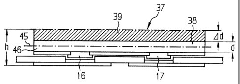
comprising the chip 38 of reduced thickness. As is to be
indicated by the shaded subsidiary area in Figure 2,
following the material-removing processing of a surface
arranged opposite the contact metallizations 16, 17 and
referred to in the following as rear side 39, the chip 38
is to possess a thickness reduced by ~d compared to the
chip 11 shown in Figure 1, so that the thickness d of the
chip 38 is substantially smaller than the thickness D of
3 0 the chip 11 ( Figure 1 ) .
If Figure 2 is compared with Figure 3, which illustrates an
enlarged partial view of the chip module 10, it will be
apparent that the thickness reduction 0d shown in Figure 2
results in a chip module 37 with a substantially smaller
overall thickness h compared to the chip module 10 with the
overall thickness H.
CA 02274785 1999-06-09
11
In the form of the example of a connection point, Figures 3
and 4 illustrate the manner in which the connection between
the contact metallization 17 and the connecting lead 15 of
the substrate 12 is established to form the chip module 10.
It can clearly be seen how, commencing from a covering
layer with associated recess 19, the contact metallization
17 engages into the recess 19 formed in the carrier layer
13 in the region of the contact metallization 17. The
recess 19 in the carrier layer 13 extends up to the
connecting lead 15 arranged on the rear side of the'carrier
layer 13 facing towards the chip 11 and leaves said
connecting lead 15 exposed in the region of a rear chip
contact zone 21 arranged opposite an outer contact side 20.
The recess 19 contains a connecting material 22 which
serves both to establish an electrically conductive
connection between the contact metallization 17 and the
chip contact region 21 of the connecting lead 15 and to
establish a mechanically reliable connection between the
chip 11 and the substrate 12.
The connecting material 22 illustrated in Figures 3 and 4
consists of a solder coating in solid form applied to the
chip contact region 21 of the connecting lead 15. The
solder composition selected for the solder coating here is
adapted to the alloy or material composition used for the
contact metallization 17. When gold is used for the
contact metallization 17, a lead/tin solder is suitable as
connecting material. In place of the solder coating it is
also possible, for example, to use an electrically
conductive epoxide-resin-based adhesive or a thermoplastic
adhesive.
In any case, regardless of the nature of the connecting
material, the connection illustrated in Figure 3 between
the contact metallization 17 and the chip contact region 21
of the connecting lead 15 is established by the
CA 02274785 1999-06-09
1,:~ :::
12
introduction (arrow 48 in Figure 4) of the contact
metallization 17 into the recess 19, commencing with the
chip 11 arranged above the substrate 12 (Figure 4), with
the displacement of the connecting material 22. In order,
in the case of a connection established in this way, to
ensure a repeatable, uniform and smallest possible overall
height H of the chip module 10 formed by the chip 11 and
substrate 12, it is sufficient to introduce the contact
metallization 17 into the recess 19 until the passivation
layer 18 of the chip 11 bears against the surface of the
carrier layer 13 facing towards the chip 11. To further
improve the mechanical connection between the chip 11 and
substrate 12 effected via the connecting material 22 and
illustrated in Figure 1 in the case of the example of the
contact metallization 17, as indicated in Figure 1 it is
possible to provide further metallization projections 35,
36 in addition to the contact metallizations 16, 17 serving
for the electrical contacting of the substrate 12, which
further projections 35, 36 are formed similarly to the
contact metallizations 16, 17 and are inserted into fixing
recesses which correspond in form to the recesses 19 but
have not been shown in detail here. Here again, precisely
as in the case of the contact metallizations 16, 17, a
connection is established between the metallization
projections 35, 36 and the connecting leads 14, 15,
although this connection serves merely for the mechanical
fixing of the chip on the substrate and does not have any
electrical contact function. To assist the adhesion of the
chip 11 on the substrate 12, planar or peripheral adhesion
of the chip 11 on the substrate 12 can also be provided.
As can be clearly seen from Figure 3, even in the case of
the only partial recessing of the contact metallization 17
into the connecting material 22, wetting occurs of all the
exposed sides of the contact metallization 17, here shown
in simplified form as a parallelepiped. This leads to
correspondingly small electrical resistances in the contact
CA 02274785 1999-06-09
13
region of the contact metallization 17 and the connecting
material 22 and to good mechanical adhesion.
In order to prevent the formation of pressure cushions due
to compression effects in the recess 19, especially when
the recess 19 is plentifully filled with connecting
material 22, on its upper side facing towards the chip the
carrier layer 13 of the substrate 12 can be provided with a
groove-like ventilating channel 23 leading outwards from
the recess 19 or with other suitable devices.
In addition to the insulating layer formed as carrier layer
13 and illustrated in Figure 1, a further insulating layer,
which covers the connecting leads at least except for
contact recesses, can also be arranged on said connecting
leads. Additionally, the chip module 10 can also be
provided with a coil arranged on the substrate to form a
transponder.
The softening of the connecting material or melting of the
connecting material required for the recessing of the
contact metallization 17 into the connecting material 22
can take place simultaneously to the application of the
pressure required for the displacement of the connecting
material, as illustrated for example in Figure 5. Figure 5
shows a chip module production device 24 with two
components combined in a stationary device, namely a chip
placement device 25 and a heating device 26. As can be
seen from Figure 5, the chip 11 is moved from above, with
its contact metallizations 16, 17 facing downwards, towards
the substrate 12 here arranged in a substrate strip 27.
The contact metallizations 16, 17 are now brought to bear
against the connecting material 22 arranged in the recesses
19 in the chip contact region 21 (Fig. 3? of the connecting
leads 14, 15. During the contacting of the contact
metallizations 16, 17 with the connecting material 22,
contact heating of the connecting leads 14, 15 can be
CA 02274785 1999-06-09
14
effected by means of the heating device 26, which is moved
from below the substrate strip 27 towards the particular
substrate 12. Under the pressure of the chip placement
device 25, the contact metallizations 16, 17 then penetrate
into the connecting material 22 softening under the effect
of the heat.
As an alternative to heating the connecting material 22
during the placement of the chip 11 as described in the
foregoing, it is also possible to melt the connecting
material 22 in a reflow process following the placement of
the chip 11, and thus to effect the wetting of the contact
metallizations required for the connection of the
connecting material 22 to the contact metallizations 16,
17. Depending upon the nature of the connecting material,
here it can be necessary to overcome the boundary surface
resistance of the connecting material 22 by applying
pressure to the contact metallizations 16, 17 using an
additional pressure device downstream of the chip placement
device 25, in order to facilitate the recessing of the
contact metallizations 16, 17 into the connecting material
22 so as to achieve the described embedding of the contact
metallizations 16, 17 in the connecting material 22.
Figure 6 is a plan view of the substrate strip 27 already
mentioned in association with the chip module production
device 24 illustrated in Figure 5. As can be seen from the
plan view, the substrate strip 27 comprises a plurality of
continuously, consecutively formed substrates 12 connected
to one another via their connecting leads 14, 15 extending
over the substrates. In order to separate an individual
substrate 11, as shown in Figure 1, from the substrate
strip 27 i~t is only necessary to perform a punching process
along the punching lines 47 represented in dash-dotted
manner in Figure 5. The punching process serves to sever
connecting regions 29, 30 of the connecting leads 14, 15
and outer edges 32, 33 of the substrate strip 27 which form
CA 02274785 1999-06-09
traction edges and are provided with a perforation 31.
Such a design of the substrate strip 27 facilitates the
continuous production of chip modules l0 wherein, as
illustrated in Figure 5, the substrate strip 27 with the
5 substrates 12 provided therein is conducted past the chip
placement device 25 in the feed direction 34 in clock-
controlled manner.
The chip modules 10 produced in the chip module production
10 device 24 in each case constitute an intermediate product
or handling unit for the subsequent processing of the chips
11 with the goal of producing chip modules 37 comprising
chips 38 which are thinner than the chips 11. By virtue of
the composite formed by the substrate strip, the chip
15 modules 10 in their totality form a corresponding handling
composite. Prior to the separation of the chip modules 10
from the substrate strip 27 explained in the foregoing, as
illustrated in Figure 5 in the example of a continuous
production process, material-removing processing of the
chips 11 of the chip modules 10 takes place following their
production in the chip module production device 24. For
this purpose the chip modules 10 are fed to a processing
device 40 in which chip body material is removed from the
rear side 39 of the chip 11, as schematically illustrated
in Figure 2. In the processing operation illustrated by
way of example in Figure 5, the processing device consists
of a belt grinding device 40 comprising an endless grinding
belt 43 continuously revolving via rollers 42 on a device
carrier 41. The device carrier 41 is provided with an
adjusting device, not shown in detail here, which enables
the device carrier 41 to be moved upwards and downwards in
the direction of the double arrow 44. By superimposing an
adjusting movement, directed towards the rear side 39 of
the chip~ll, upon the revolving movement of the grinding
belt 43, the chip 11 can be continuously reduced in its
thickness until a chip 38 is obtained having a thickness d
reduced compared to that of the original chip 11 (Figure
CA 02274785 1999-06-09
16
2). The thickness d attainable by means of this processing
is limited by the boundary layer 45, indicated in dash-
dotted lines in Figure 2, which delimits a circuit region
46 of the chip situated between the passivation layer 18
and the boundary layer 45. Until the boundary layer 45 is
reached, the chip can be processed from its rear side 39
without impairing the function of the chip due to
penetration into the circuit region 46.
The processing of the chip 11 with the belt grinding device
40 as illustrated in Figure 5 gives rise to the chip module
37 illustrated in Figure 2, which has a substantially
reduced overall height h compared to the starting chip
module 10. The chip modules 37 of reduced thickness
continuously produced in accordance with the process
illustrated in Figure 5 can then be separated from the
composite substrate strip 27 as described in the foregoing
with reference to Figure 6.