Note: Descriptions are shown in the official language in which they were submitted.
CA 02274828 2005-05-18
-1-
LIGHTING APPARATUS HAVING LOW PROFILE
Background of the Invention
The present invention relates to a lighting apparatus. More particularly, the
present
invention relates to a low profile lighting apparatus utilizing a waveguide
for illumination. The
invention is particularly advantageous for use as a backlight for illuminating
a display.
Backlights may be used to illuminate both mechanical displays, such as on
analog
watches or automobile gauges, as well as electronic displays, such as liquid
crystal displays
used with cellular phones, and pagers, and personal digital assistants.
Because many
backlight applications involve smaller displays where space is at a premium,
it is desirable to
reduce the thickness of such backlights while still maintaining the area of
illumination.
Backlights thus require reduced aspect ratios, defined as the ratio of the
thickness of the
backlight to the length of the illumination area.
One type of a backlight utilizes of a light source, such as a light-emitting
diode (LED),
that is coupled to a waveguide into which light is injected. The light source
is typically
mounted at an outer peripheral edge of the waveguide and is energized to emit
light into the
waveguide. The light undergoes several reflections between the surfaces of the
waveguide
until being transmitted through a top surface to illuminate the display.
One difficulty associated with such backlights is they do not produce a
uniform
intensity across the surface of the waveguide. The light loses intensity as it
propagates
outward from the light source. Consequently, as the distance from the light
source increases,
the intensity of the light transmitted out of the waveguide decreases. This
results in the
portions of the waveguide distal of the light source having reduced intensity.
There is therefore a need for an efficient backlight having a low aspect ratio
that
provides a substantially uniform illumination profile across the entire area
of illumination.
Summary of the Invention
In accordance with one aspect of the invention, there is provided an
illumination and
display device. The device includes an optical waveguiding layer and
Illumination coupling
means embedded in an interior region of the waveguiding layer, wherein the
illumination
coupling means includes one or more semiconductor light emitting devices. A
portion of the
optical waveguiding layer has a pair of symmetric (a) nonplanar, curved
surfaces, or (b) a
plurality of flat, planar surfaces approximating the nonplanar, curved
surface, the pair of
symmetric surfaces forming a cusp lying on the axis of the one or more
semiconductor light
emitting devices to produce total internal reflection of light from the one or
more
semiconductor light emitting devices into the waveguiding layer. The
illumination and display
device further includes display elements formed on surfaces of the waveguiding
layer to
cause light to be emitted from the waveguiding layer.
CA 02274828 2005-05-18
_2_
The display elements may be formed as concave channels within the surface of
the
waveguiding layer, and external surfaces of the channels are either smooth or
rough to
promote diffuse output radiation.
The illumination from the display elements may be controlled by varying the
depths of
the concave channels of the display elements across the waveguiding layer in
order to
compensate for differences in illumination.
The concave channels of the display elements may be deeper towards the outer
portions on the waveguiding layer of the display device than are the concave
channels
towards the central portions of the waveguiding layer of the display device.
Each of the display elements may be formed as an extractive display element on
a
waveguiding cylinder, each of the extractive display elements being formed as
a polygon solid
having an apex or a vertex on a line normal to the waveguiding layer, and
light from the
waveguiding layer is transmitted by total internal reflection within both the
waveguiding
cylinder and by side faces of the extractive display element to be emitted at
the apex or the
vertex of the extractive display element.
Each of the extractive display elements may have the form of a polygon solid
having
two or more equilateral side faces.
The illumination from the display elements may be controlled by varying the
diameters of the waveguiding cylinders of the display elements across the
waveguiding layer
in order to compensate for differences in the illumination.
The waveguiding cylinders of the display elements may have diameters that are
larger towards the outer portions on the waveguiding layer of the display
device than are the
waveguiding cylinders towards the central portions of the waveguiding layer of
the display
device.
Each of the display elements may be formed as an extractive display element on
the
waveguiding layer, each of the extractive display elements may be formed as a
polygon solid
having an apex or a vertex, and light from the waveguiding layer may be
transmitted by total
internal reflection by side faces of the extractive display element to be
emitted at the apex or
the vertex of the extractive display element.
The illumination from the display elements may be controlled by varying the
sizes of
the polygon solids on the waveguiding cylinders of the display elements across
the
waveguiding layer in order to compensate for differences in the illumination.
The convex or concave lens element may be incorporated integrally to the
surface of
the waveguiding layer adjacent to the interior region at a location where the
illumination
coupling means is embedded in the waveguiding layer with an air gap between
the
semiconductor light emitting devices and the lens element.
The symmetric, nonplanar, curved surface may have a shape that is a section of
an
equiangular spiral.
CA 02274828 2005-05-18
-3-
The symmetric, nonplanar, curved surface may have a shape that is a section of
a
parabola, a hyperbola, a circle, or a sine curve.
The device may be used as a display for an exit sign, an automobile tail
light, or the
face of a watch or clock.
The one or more semiconductor light emitting devices at the illumination
coupling
means may be embedded in the waveguiding layer by optically coupling the one
or more
semiconductor light emitting devices to the waveguiding layer with an optical
coupling agent.
The optical coupling agent may be one of a silicone adhesive, gel, grease or
an
epoxy polymer.
The waveguiding layer may have an overall shape that is thin relative to its
length,
and is flat or curved.
The display elements may be arranged in either symbolic alphanumeric patterns
or
nonsymbolic patterns.
The illumination from the display elements may be controlled by changing a
characteristic of the display elements across the display device.
The one or more semiconductor light emitting devices may be bullet lens
package
light emitting diodes or bare light emitting diodes.
In accordance with another aspect of the invention, there is provided an
illumination
and display device. The device includes an optical waveguiding layer,
illumination coupling
means embedded in an interior region of the waveguiding layer, wherein the
illumination
coupling means includes one or more semiconductor light emitting devices and
display
elements formed on the surface of the waveguiding layer to cause light to be
emitted from the
waveguiding layer.
In accordance with another aspect of the invention, there is provided an
illumination
and display device. The device includes an optical waveguiding layer,
illumination coupling
means embedded in an interior region of the waveguiding layer, wherein the
illumination
coupling means includes one or more semiconductor light emitting devices, each
of the one
or more semiconductor light emitting devices having a longitudinal axis that
is parallel to the
surface of the optical waveguiding layer, the illumination coupling means
including a hole or
recess in the interior region of the waveguiding layer where the one or more
semiconductor
light emitting devices is placed and display elements formed on the surface of
the
waveguiding layer to cause light to be emitted from the waveguiding layer.
The plurality of the semiconductor light emitting devices may be arranged
around the
perimeter of a circle in the interior region of the waveguiding layer.
The display elements may be formed as concave channels within the surface of
the
waveguiding layer, and external surfaces of the channels may be either smooth
or rough to
promote diffuse output radiation.
CA 02274828 2005-05-18
-4-
The illumination from the display elements may be controlled by varying the
depths of
the concave channels of the display elements across the waveguiding layer in
order to
compensate for differences in the illumination.
The concave channels of the display elements may be deeper towards the outer
portions on the waveguiding layer of the display device than are the concave
channels
towards the central portions of the waveguiding layer of the display device.
Each of the display elements may be formed as an extractive display element on
a
waveguiding cylinder, each of the extractive display elements may be formed as
a solid
polygon having an apex or a vertex on a line normal to the waveguiding layer,
and light from
the waveguiding layer may be transmitted by total internal reflection within
both the
waveguiding cylinder and by side faces of the extractive display element to be
emitted at the
apex or the vertex of the extractive display element.
Each of the extractive display elements may have the form of a solid polygon
having
two or more equilateral side faces.
One aspect of the present invention relates to a lighting apparatus for
illuminating an
illumination area of a display. The lighting apparatus comprises a waveguide
adapted for
mounting adjacent the display so as to illuminate the illumination area of the
display. The
waveguide comprises a top surface having an optical output area corresponding
in size to the
illumination area, a bottom surface spaced apart from the top surface, and a
side surface
extending between the top and bottom surfaces. Reflective material is
positioned adjacent the
bottom and side surfaces of the waveguide. At least one light source is
mounted to input light
proximate to a periphery of the waveguide between the top and bottom surfaces.
The
waveguide further comprises a light ejector on one of the top and bottom
surfaces configured
to redirect light propagating between the surfaces towards the top surface for
transmission
therethrough. The light ejector is arranged to provide a preselected
illumination profile across
the optical output area of the top surface.
Another aspect of the invention relates to a lighting apparatus comprising a
waveguide having pair of opposed surfaces. Each of the surfaces is at feast
partially reflective
and at least one of the surfaces is partially transmissive. Each of the
surfaces have a
reflectivity greater than the transmissivity of the at least one surface.
Another aspect of the invention relates to a lighting apparatus comprising a
planar
waveguide having a peripheral edge and a light source mounted proximate to the
peripheral
edge so as to direct light into the waveguide along a path extending from the
light source
towards an optical diverter in the waveguide. The optical diverter in the path
redirects light
rays away from the path towards the periphery of the waveguide.
Yet another aspect of the invention relates to a lighting apparatus comprising
a top
surface, a bottom surface in spaced relationship to the top surface and
cooperating with the
top surface to form a waveguide having a thickness defined by the distance
between the top
and bottom surfaces, and at least one solid state point light source mounted
to input light into
CA 02274828 2005-05-18
-4a-
the waveguide between the surfaces. One of the surfaces has a curvature
relative to the other
surface which yields a substantial variation in the thickness of the waveguide
in a selected
region of the waveguide. The variation follows a geometric contour selected to
redirect light
propagating between the surfaces of the waveguide so that the redirected light
exits the top
surface of the waveguide.
Another aspect of the invention relates to a lighting apparatus comprising a
waveguide having top and bottom surfaces and a peripheral edge. The waveguide
has a
thickness defined by the distance between the top and bottom surfaces. The
thickness at the
peripheral edge is substantially different than the thickness in a region
intermediate opposing
sides of the peripheral edge. The thickness has a geometry selected to enhance
ejection of
light from the top surface intermediate the opposing sides. At least one light
source is
disposed proximate to the peripheral edge to introduce light into the
waveguide between the
top and bottom surfaces.
Yet another aspect of the invention relates to a lighting apparatus comprising
a
waveguide of solid material the waveguide having a top surface, a bottom
surface and a side
surface. A light source is mounted to input light into the waveguide and
reflective material is
juxtaposed with one of the top and bottom surfaces wherein at least a portion
of one of the
top and bottom surfaces has a pattern of elongate structures that generally
increase in
density with distance from the light source.
A further aspect of the invention is directed to an illumination device
comprising a
waveguide having an illumination coupler embedded in an interior region
thereof. The
waveguide has generally parallel top and bottom surfaces outside of the
interior region such
that light is guided therebetween. The illumination coupler comprises a
refractive index
interface configured to capture light rays propagating along a line that forms
less than the
critical angle of total internal reflection with respect to at least one of
the top and bottom
surfaces, such that the captured light rays are injected therebetween for
propagation outside
of the interior region. In one embodiment the illumination coupler comprises a
surface
configured for total internal reflection of light incident thereon. The
illumination coupler of this
embodiment is integrally formed with the waveguide from a single piece of
transparent
material, and the reflecting surface is uncoated. A point source of light is
disposed at least
partially, preferably fully within a cavity formed in the waveguide adjacent
the total internal
reflecting surface. Display elements may be included on at least one of the
surfaces for
ejecting light from the waveguide. Additionally, diffusive reflective material
may be included on
at least one of the top and bottom surfaces.
In yet another aspect of the invention, there is disclosed a lighting
apparatus,
comprising a device that emits light and an optical cavity that is formed by
diffusive reflective
surfaces, the cavity having an output region through which light from the
cavity passes. The
light emitting device is mounted to supply light to the cavity while being
hidden from direct
view through the output region. The cavity has a diffusely reflective surface
area and the
CA 02274828 2005-05-18
-4b-
output region also has an area. The ratio of the area of the output region to
the sum of (i) the
area of the output region and (ii) the surface area of the cavity is at least
0.05. Additionally,
the cavity has a depth and the output region has an edge to edge bisector
dimension, the
ratio of the depth to the bisector dimension being significantly less than
0.1. The lighting
apparatus additionally comprises an angular spectrum restrictor positioned to
restrict output
illumination through the output region to a predetermined range of angles.
Another aspect of the invention involves a method of lighting. The method
comprises
producing illumination from an optical cavity formed by diffusely reflecting
surfaces and
outputting illumination from the cavity through an output illumination region.
Producing of the
illumination comprises directing light rays from a source of illumination into
the cavity such
that the source of the illumination is not visible through the output
illumination region. The
method further comprises restricting the angular spectrum of illumination from
the output
illumination region to a predetermined range of angles, and mounting the
optical cavity to
illuminate at least a portion of a room.
In another aspect of the invention, there is disclosed a method of
manufacturing a
lighting apparatus. One embodiment of the method comprises wrapping a flexible
sheet of
reflective material around one side of a tubular light source, juxtaposing a
member forming an
optical cavity with another side of the tubular light source so that light
from the source is
introduced into the optical cavity, and attaching the flexible sheet to the
member such that the
sheet retains the tubular source in juxtaposition with the member.
Brief Description of the Drawings
These and other features of the invention will now be described with reference
to the
drawings of a preferred embodiment, which are intended to illustrate and not
to limit the
invention, and in which:
Figure 1 is a perspective view of wristwatch incorporating one embodiment of a
lighting apparatus;
Figure 1A is a cross-sectional view of the watch of Figure 1 taken along line
1A-1A;
Figure 2 is a top plan view of the lighting apparatus used to illuminate the
watch of
Figure 1;
Figure 3 is a cross-sectional side view of the lighting apparatus of Figure 2
taken
along the line 3-3;
Figure 4 is a cross-sectional view of the lighting apparatus of Figure 2 taken
along the
line 4-4;
Figure 4A is an enlarged view of a portion of Figure 4;
Figure 4B is a cross-sectional view similar to that of Figure 4, but with
elongate
structures on the top surface;
Figure 4C is a cross-sectional view similar to that of Figure 4, but with
reflective
material surrounding the entire waveguide;
CA 02274828 2005-05-18
-4c-
Figure 5 is a top plan view of an alternative embodiment of a waveguide for
use in the
lighting apparatus of Figure 2;
Figure 6 is a top plan view of yet another embodiment of a waveguide for use
in the
lighting apparatus of Figure 2;
Figure 7 is a top plan view of yet another embodiment of a waveguide for use
in a
lighting apparatus;
Figure 8 is a top plan view of a waveguide showing another embodiment of an
optical
d iverter;
Figure 9 is a cross-sectional view of a lighting apparatus used with a light
enhancing
structure;
Figure 10 is a top plan view of a waveguide having a dimple for redirecting
light rays;
Figure 11 is a cross-sectional side view of the lighting apparatus of Figure
10 taken
along the line 11-11;
Figure 12 is a perspective view of an alternate embodiment of a lighting
apparatus;
Figure 13 is a cross-sectional view of the lighting apparatus of Figure 12;
Figure 14 is a perspective view of a housing used with the lighting apparatus
of
Figure 12;
Figure 15 is a perspective view of a lighting apparatus including a total
internal
reflection region;
Figure 16 is cross-section view of the lighting apparatus of Figure 15 taken
along the
line 16-16;
Figure 16A is an enlarged view of a portion of Figure 16;
Figure 17 is a perspective view of an alternative embodiment of a lighting
apparatus
including a total internal reflection region;
Figure 18 is a cross-sectional view of the lighting apparatus of Figure 17
taken along
the line 18-18;
CA 02274828 1999-06-11
WO 98/26212 PCT/US97/22742
-5-
Figure 19 is a schematic side view of a prior art "bullet lens" tED;
Figure 20 is a schematic side view of a prior art "bare" LED;
Figure 21 is a perspective view of an exit sign incorporating an alternative
embodiment of a lighting
apparatus;
Figure 22 is a rear perspective view of an automobile having taillights that
incorporate a lighting apparatus;
Figure 23 is a top view of a wrist watch incorporating an alternative
embodiment of a lighting apparatus;
Figure 24 is a cross-sectional side view of the exit sign of Figure 21 taken
along the line 24-24;
Figure 25 is a perspective view of an exit sign incorporating yet another
embodiment of a lighting
apparatus;
Figure 26 is a side view of an exit sign incorporating extractive display
elements;
Figure 27 is a side view of an extractive display element;
Figure 28 is a side view of an alternative embodiment of an extractive display
element;
Figure 29 is a perspective view of an exit sign incorporating circular grooves
for extracting light; and
Figure 30 is a cross-sectional side view of the exit sign of Figure 29.
Detailed Descriotion of the Preferred Embodiment
Referring to Figures 1 and 1A, one embodiment of the present invention is
utilized as a back lighting
apparatus 26 for a wristwatch 20. Although the wristwatch 20 is shown having a
generally circular shape, it will
be appreciated that the wristwatch may have any of a variety of shapes.
Art outer housing 22 of the wristwatch 20 encloses a thin disk 30 of
substantially transparent material
that is spaced below a watch crystal 24. The disk 30 has an upper display
surface 32 and an opposed bottom
surface 34. The display surface 32 includes indicia 35 (Figure 1), such as
numerals for indicating time, although
other indicia could also be displayed. Two hands 36 of the watch 20 are
mounted for rotation about a stem 38
that extends through the disk 30. The stem is driven by a watch mechanism 40
in a well known manner.
Alternatively, the disk 30 may comprise a liquid crystal display in which
indicia, such as the hands and numerals,
are electrically generated.
Referring to Figure 1 A, the lighting apparatus 26 is interposed between the
disk 30 and watch mechanism
40 for illuminating the disk 30. The lighting apparatus 26, which is
preferably in contact with the disk 30, includes
a waveguide 42 and a tight source 44 positioned along a peripheral edge of the
waveguide 42.
In the illustrated embodiment, the housing 22 supports the disk 30 and the
lighting apparatus 26 in
juxtaposed relationship to each other. The disk 30 is mounted so that its
periphery is supported by a first annular
lip 46 which partially covers the display surface 32 to define a viewing area
or illumination region of the display
surface 32. The waveguide 42, which has a diameter slightly larger than that
of the disk 30, is mounted so that
its periphery is supported by a second annular lip 48 in the housing 22. The
second annular lip 48 is sized to shield
the light source 44 from being directly visible through the illumination
region of the display surface 32. By way of
example, the diameter of the illumination region may be 27 mm.
CA 02274828 1999-06-11
WO 98/26212 PCT/US97/22742
-6
As shown in Figure 2, the waveguide 42 has a circular shape-optimal for
illuminating a circular watch,
although other shapes may be utilized for various applications. The light
source 44 is mounted within a triangular
or V-shaped notch 50 in the peripheral edge of the waveguide 42. The notch 50
serves as an optical diverter which
redirects light uansmitted by the light source 44, utilizing refractive index
differences at the interface 52 formed by
the sides of the notch 50. In a preferred embodiment, the V-shaped optical
diverter 50 is symmetrical such that
a line passing through its apex and the center of the waveguide 42 bisects the
V-shaped notch.
In a preferred embodiment, the light source is a single. solid state, point
source of light, such as a light
emitting diode (LED) 44 mounted on a carrier or circuit board (not shownl. The
carrier on which the LED 44 is
mounted is attached to the waveguide at the back of the notch 50 (i.e., the
open end opposite the apex) utilizing
an adhesive (not shownl. The LED 44, which is typically in the form of a cube
of solid state material that emits
light from each of multiple faces (i.e., its top surface and four sided, is
spaced from the sides of the notch 50 with
air therebetween. The difference in index of refraction between the waveguide
and the air creates the refractive
index interface 52 that causes light to refract as the light passes into the
waveguide 42. In accordance with this
advantageous feature, a substantial fraction of the light passing through the
interface 52 is refracted toward
opposite sides of the waveguide 42 (i.e., the sides generally adjacent to and
on opposite sides of the light source
441. in this manner, regions of the waveguide 42 that are located to the sides
of the light source 44 are efficiently
illuminated, and the diverter 50 thereby contributes to uniform illumination.
The waveguide 42 is preferably comprised of a material that is transparent to
light produced by the LED
44, such as a transparent polymeric materiat, and may be manufactured by
various well-known methods, such as
machining or injection molding. Preferred materials for the waveguide 42 are
acrylic, polycarbonate, and silicone.
Acrylic, which has an index of refraction of approximately 1.5, is scratch
resistant and has a lower cost relative to
polycarbonate. Polycarbonate, which has an index of refraction of
approximately 1.59, has higher temperature
capabilities than acrylic. Polycarbonate also has improved mechanical
capabilities over acrylic. Silicone has a
refractive index of approximately 1.43. The refractive index of air is 1Ø
The dimensions of the waveguide 42 may
vary, although the waveguide 42 is desirably very thin relative to its length
so as to provide a low profile. The
distance between the top surface 56 and the bottom surface 58 is preferably on
the order of 1-3 mm, while the
diameter of the waveguide 42 is typically at least 2.0 mm.
As shown in Figure 2, a plurality of display elements comprising elongate
structures 54 extend across the
waveguide 42 for redirecting light propagating within the waveguide 42.
Although illustrated as lines, the elongate
structures 54 have a three-dimensional shape, as described in detail below. In
the illustrated embodiment, the
elongated elongate structures 54 are arranged in a pattern consisting of
intersecting lines that extend radially
outward from a common point at the center of the waveguide 42 through which
the stem 38 passes. The elongate
structures 54 are preferably spaced apart by an equal angular distance, such
as 0.3 degrees. It has been found that
the pattern of radial grooves utilized in the watch 20 are highly effective in
eliminating "shadows" that would
otherwise be cast by the watch stem 38.
_~.____._ _. _. __
CA 02274828 1999-06-11
WO 98/26212 PCT/ITS97/22742
.7.
As illustrated in Figure 3 the waveguide 42 includes atop surface 56 and an
opposed bottom surface 58,
which are substantially parallel to each other. A side or edge surface 60
extends between the top and bottom
surfaces 56, 58 along the periphery of the waveguide 42. While the surfaces
56, 58 are typically flat for backlight
applications, the surfaces 56, 58 may also be formed as curved surfaces, such
as when the waveguide is utilized
as a taillight for an automobile.
A diffusive reflective material 62 is positioned adjacent the bottom surface
58 and side surface 60 of the
waveguide 42, with the material 62 also preferably covering a peripheral strip
61 on the top surface 56. In the
embodiment illustrated, the peripheral strip 61 is sufficiently wide to cover
the notch 50 so that the top, the bottom,
and the outside edge of the notch 50 are covered by the reflective material
62. The peripheral strip is also
preferably sufficiently wide that the LED 44 cannot be viewed directly ftom
viewing angles of 75 degrees or less
lit being understood that the viewing angle is measured from a fine normal to
the top surface 561. By way of
example, the peripheral strip may be equal in width to the width of the second
annular lip 48 of the watch 20
(Figure 1 ).
The diffusive reflective material 62, which has a reflectivity of at least B8%
may comprise a single layer
or multiple layers of diffusely reflective tape, such as DRP"" Backlight
Reflector, manufactured by W.L. Gore &
Associates. DRP"' Backlight Reflector has a reflectivity of approximately 97%-
99.5%, depending on its thickness
and the wavelength of the light. Alternatively, the reflective material 62
could comprise a paint or coating that is
applied to the surfaces 58 and 60, such as white house paint or a more exotic
material, such as the Labsphere
Corporation's Spectraflect paint. Spectraflect paint's reflectivity is
considerably higher than house paint, roughly
98%, while the reflectivity of a good white house paint is approximately 90%.
Because the reflective material 62 covers the bottom and side surfaces 58, 60,
as well as the peripheral
strip on the top surface 56, light will be emitted from the waveguide in an
output illumination region or aperture 65
comprising the central uncovered portion of the top surface 56 (i.e., the
portion of the surface 56 interior to the
peripheral strip 611. It will be appreciated that light rays incident on the
top surface 56 at an angle of incidence
(i.e., the angle of the ray relative to a line normal to the surface) at least
equal to a critical angle will be totally
internally reflected toward the bottom surface 58. That is, the top surface 56
will reflect all of such light back into
the waveguide 42. Light rays having an angle of incidence less than the
critical angle are transmitted through the
top surface 56. The value of the critical angle is dependent on the difference
in the indices of refraction between
the waveguide 42 and the disk 22, as is known by those skilled in the art. For
a waveguide 42 having a refractive
index of 1.5, the critical angle is approximately 42° when surrounded
by air.
As shown in Figures 4 and 4A, the elongate structures 54 may comprise grooves
defined by surfaces 64
(Figure 4A) that form a substantially triangular or U-shaped cross-section.
The elongate structures 54 advantageously
alter the angle of incidence of light reflected toward the top surface 56 to
enhance passage therethrough. That is,
the angled surfaces fi4 reflect light toward the top surface 56 at an angle of
incidence less than the critical angle
so that such light passes through the top surface 56 rather than being totally
internally reflected. The elongate
structures 54 are thus used to "eject" light rays that might otherwise be
totally internally reflected by the top
CA 02274828 1999-06-11
WO 98/26212 PCT/US97/22742
.g.
surface 56. This advantageously increases the optical efficiency of the
waveguide 42 by ejecting light that would
otherwise experience energy loss through repeated reflections. The elongate
structures are defined by a depth D
and an apex angle 8 that bisects the V-shaped structure 54. In the preferred
embodiment, depth D is in the range
of 1-2 micrometers and the angle B is approximately equal to 45 degrees.
Preferably, an air gap is maintained within
the V-shaped structure 54 (i.e., the grooves are not filled with reflective
materiall.
The elongate structures 54 are preferably arranged to achieve generally
uniform illumination profiles across
the illumination output region of the waveguide. In preferred embodiments, the
uniformity ratio of the output
illumination region, which is defined as the ratio of the highest intensity to
lowest illumination within such region
is no more than 2 to 1.
Referring to Figures 4B, in another preferred embodiment, the elongate
structures 54 are placed on the top
surface 56 instead of the bottom surface 58. The remaining aspects of this
embodiment are identical to those of
the embodiment shown in Figure 4.
In an additional embodiment, shown in Figure 4C, the entire waveguide,
including the top surface 56, bottom
surface 58, and side surfaces 60 are covered by reflective material 63, which
is preferably the same diffusely
reflecting type as the material 62, but is partially transmissive and
partially reflective. Additionally, the material 63
has a reflectivity that is greater than its transmissivity, that is, the
reflectivity is greater than 50% and the
transmissivity is less than 509'0. In one preferred embodiment, which may be
utilized in the watch 20, the reflectivity
is about 969'o and the transmissivity is about 4%. This embodiment provides an
output illumination which is
substantially uniform, even without the elongate structures 54, although such
structures may still be desirable to
reduce shadows from the watch stem 38 IFigure 1A). This embodiment is also
advantageous in that the indica
(numerals, etc.) may be applied directly to the reflective material 63,
thereby eliminating the need for the display disk
30.
Various types of groove patterns may be utilized as to improve the uniformity
of the illumination within the
region to be illuminated, depending on the situation. Referring to Figure 5,
the elongate structures 54 may be
arranged in a pattern of nonintersecting arcuate lines that are arranged about
the light source 44. In a preferred
embodiment, the radius of curvature of the arcuate fines increases with
distance from the point source 44.
Additionally, the centers of the radius of curvature lie along a line passing
through the point source and the center
of the illumination region of the waveguide, with all such centers lying along
such line Ion the side of the waveguide
that is further from the waveguide center than from the source 44). The
arcuate lines are nonuniformiy spaced apart
to compensate far loss of intensity as the light propagates outwardly from the
light source 44. Specifically, the
spacing between the elongate structures 54 decreases as the distance from the
light source 44 increases so that
the density of the elongate structures 54 increases moving away from the light
source 44. The increased density
of elongate structures 54 desirably increases the ejection of light rays in
these areas to compensate for the distance
from the source 44.
As shown in Figure 6, the elongate structures 54 could also be arranged in a
more complex pattern
comprised of a combination of simpler patterns. For example, the patterns
could take the form of arcuate lines that
CA 02274828 1999-06-11
WO 98/26212 PCT/US97/22742
-9
emanate outward from the light source 44 and straight lines that extend
radially outward from the center of the
waveguide 42.
Figure 7 shows a rectangular-shaped waveguide 42. Such a waveguide is
preferably used to illuminate a
rectangular-shaped display, such as on cellular phones or personal digital
assistants. Although reflective material is
not shown, it will be understood that this embodiment may be constructed in
the manner previously described. In
the illustrated embodiment, multiple point light sources 44 are coupled to
introduce light at spaced peripheral
locations along the edge of the waveguide 42. Because multiple sources are
employed, optical diverters such as the
notch 50 are optional, and may or may not be included. The elongate structures
54 of this embodiment are arranged
in concentric arcs around each of the light sources 44, although various other
patterns are contemplated, including
those discussed above.
Figure 8 illustrates an alternative embodiment in which elongate structures 54
are formed in a waveguide
42a by scratching a top or bottom surface of the waveguide with an abrasive,
such as sandpaper. The abrading
is preferably non uniform such that the density of the scratches or grooves
increase with distance from the light
source 44. By way of specific example, in the rectangular waveguide shown in
Figure 8, the grooves are directed
along the length of the rectangle, rather than the width. The groove pattern
is generally amorphous on a local basis,
but is substantially directional and nonrandom on a global basis.
Figure 8 also illustrates an alternative embodiment of an optical diverter
that is formed by a triangular
opening 50a that extends through a waveguide 42a at its periphery. The opening
is between the light source 44
and the output illumination region of the waveguide 42. and a line drawn
between the source and the center of such
region bisects the triangle while passing through its apex. As shown, the
triangular opening 50a has two sides
which intersect at a location proximate to the light source to form such apex.
The triangular opening 50a is filled with a material, such as air, which has a
refractive index significantly
different from that of the material of the waveguide 42. The shape of the
optical diverter 50a and the refractive
index difference cause Light emanating from the light source 44 to intersect
the optical diverter 50a at an angle of
incidence which results in total internal reflection of the light towards
opposite sides of the waveguide 42. Thus,
the optical diverter 50a, tike the notch 50, redirects the path of light rays
to regions of the waveguide that are on
opposite sides of the light source 44.
Referring to Figure 9, the top surface 56 of the wave guide 42 for alternative
embodiments thereof) may
be covered with an angular spectrum restrictor 72 that restricts the output
radiation pattern from the output
illumination region 65 of the waveguide to a predetermined range of angles (in
this context, the term "spectrum" is
used in the sense of an angular spectrum rather than a wavelength spectrum).
The angular spectrum restrictor 72
comprises a planar micro-replicated optical structure, such as a holographic
diffuser, binary diffractive diffuser, or
array of microlenses. In the preferred embodiment, the angular spectrum
restrictor 72 comprises a brightness
enhancing film (BEF) which, in addition to restricting the output spectrum,
enhances the intensity of the illumination
in the output illumination region 65. The BEF 72 is preferably placed in
physical contact with a diffuser 70 to
collectively form a light quality enhancing apparatus 73. Preferably, the
diffuser 70 is disposed between the BEF
CA 02274828 1999-06-11
WO 98/26212 PCTILTS97/22742
-10
72 and the waveguide 42 and in contact with the waveguide-42. The-purpose of
the diffuser is to remove the
effect of residual nonuniformities, such as cosmetic imperfections, in the
surfaces of the waveguide 42. The diffuser
70 is comprised of translucent material, typically a thin plastic surface or
volume diffuser, both of which are
characterized by very tow absorption and minimum energy losses.
As mentioned above, the BEF 72 restricts output illumination within defined
boundary lines and also
increases the brightness within the output illumination region 65. In the
preferred embodiment, the BEF 72 is a
commercially available thin film having linear pyramidal structures, such as
3M model 90150 film. The BEF transmits
only those light rays from the waveguide that satisfy certain incidence angle
criteria with respect to the top surface
56. Alf other light rays are reflected back into the waveguide 42 toward the
bottom or side surfaces 58 and 60,
t0 respectively, where they are reflected by the reflective material 62. In
effect. the reflected rays are "recycled" until
they are incident on the BEF 72 at an angle which permits them to pass through
the BEF 72.
As is well known, a BEF, such as the BEF 72, concentrates illumination within
boundaries defined by a pair
of mutually inclined planes (which in cross-section form a "V") and does not
provide concentration in the orthogonal
direction. In some applications of the invention, it is preferable to
concentrate the illumination two orthogonal
directions, and for such applications, a second BEF oriented orthogonally to
the first BEF, may be included. With
two crossed BEFs, the emission from the waveguide wilt be within boundaries
resembling a truncated inverted cone.
As is conventional in the art, the boundaries are defined by the full-width,
half-maximum (FWHM) of the optical
intensity. By way of example, the boundaries of the cone may be inclined
relative to a line normal to the top surface
56 by an angle of no more than about 35 degrees, in which case the
illumination will be visible only within viewing
angles of 35 degrees or less.
Figures 10 and 11 illustrate a top and a cross-sectional side view,
respectively, of yet another embodiment
of the lighting apparatus 26 that utilizes a waveguide 42b. As shown in Figure
10, a light source 44 is mounted
adjacent an optical diverter 50 and the waveguide 42b is covered with
reflective material 62 or 63 in the manner
described above with respect to the waveguide 42 shown in Figures 2-4C. The
top surface 56 of the waveguide
42b includes a depressed region or dimple 74 that redirects light rays
propagating in the waveguide 42b, as described
below. As best shown in Figure 22, the dimple 74 comprises a surface 75 of
smooth and continuous curvature
relative to the bottom surface 58 so as to define an area of reduced thickness
of the waveguide 42b. As used
herein, the "thickness" of the waveguide 42 refers to the distance between the
top surface 56 and the bottom
surface 58. In the preferred embodiment, the variation of thickness (e.g.,
depth of the dimple 74) is at least equal
to 5% of the thickness of the waveguide 42 outside the dimple 74.
The dimple 74 is preferably centrally located with respect to the periphery of
the waveguide 42, covers
an area at least 70% that of the top surface 56, and defines an elliptical
shape in a cross-section parallel to the
top surface 56. For the rectangular waveguide, shown in Figure 10, the
geometric contour of the dimple 74 defines
a super ellipse in accordance with the following equation:
(xla)" + (y~bl° - 1
) __ __...___~ _.... __-~__
CA 02274828 1999-06-11
WO 98/26212 PCT/US97/22742
.11.
where n and p are both greater than 2, a is the length of the major axis of
the ellipse, and b is the length
of the minor axis of the ellipse. As is well known, increasing the exponents n
and p above two causes the shape
of the ellipse to became less oval and more rectangular. These exponents are
preferably selected so that the curved
edges of the dimple 74 extend substantially to the edges of the output
illumination region of the waveguide.
According to an advantageous feature of the waveguide 426, the surface 75 of
the dimple 74 follows a
geometric contour that redirects light propagating between the top surface 58
and the bottom surface 58, so that
the redirected light more readily and uniformly exits the top surface 56 of
the waveguide 426. Specifically, some
light will be incident on the curved dimple surface 75 at an angle of
incidence which causes ii to refract through
the top surface 56. Light having an incident angle within the critical range
will be totally internally reflected.
Reflected light will be directed toward the bottom surface 58 or side surface
28. The reflective material 62 adjacent
these surfaces reflects the light toward the top surface 56 for transmission
therethrough. Light reflected from the
bottom surface 58 in the region of the dimple 74 will typically be incident on
the dimple surface 7517-20 at a
reduced angle of incidence which permits the light to be transmitted
therethrough. Other embodiments may utilize
multiple light sources 44 with a single and multiple dimples 74.
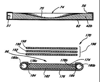
As shown in Figures 12 and 13, another embodiment of the lighting apparatus,
referred to as
lighting apparatus 170, comprises a rectangular waveguide 172 having a top
surface 174 (Figure 13) and
an opposed bottom surface i 76 (Figure 13). Four side surfaces 178a (Figure
13), 1786 (Figure 13), 178c,
and 178d extend between the top surface 174 and bottom surface 176. A pair of
lamps 180a, 1806 are
mounted adjacent the opposing side surfaces 178a and 1786. The lamps 180a,
1806 are preferably held
in place by diffusive reflective material 182 that surrounds the lamps 180a,
1806 and covers a significant
portion of the waveguide 172, as described more fully below.
The lamps 180 preferably comprise fluorescent tubes of circular cross~section
which extend along
substantially the entire length of the sides 178a, 1786. As best shown in
Figure 13, the sides 178a and
1786 of the waveguide 172 are preferably each concave to form respective
elongate channels that extend
along the entire length of the sides 178a, 1786. Such channels are configured
to flushly receive respective
surfaces on sides of the lamps 180a, 1806. An optical coupling gel 184 is
interposed between the lamps
180a, 1806 and the sides 178a, 1786 of the waveguide 172 in order to reduce
repetitive index differences
by eliminating air gaps therebetween and thereby efficiently couple light from
the lamps i80a, 1806 to the
waveguide 172. Alternatively, the lamps 180a, 1806 may each comprise a linear
array of point sources,
such as LEDs (not shownl.
In the preferred embodiment, the reflective material 182 entirely covers the
bottom surface 176
and wraps around the lamps 180a, 1806 to secure and retain them in
juxtaposition with the side surfaces
178a, 1786 of the waveguide 172. The reflective material 182 also wraps around
the sides 178c, 178d
and extends onto a portion of the top surface 174 so as to form a peripheral
strip 186 (Figure 12) that
extends around the perimeter of the top surface 174.
CA 02274828 1999-06-11
WO 98/26212 PCT/US97/22742
-12-
Accordingly, the interior surface of the reflective material creates an
optical cavity that is filled
by the solid waveguide 172 and lamps 180. The portion of the top surface 174
of the waveguide 172
that is not covered by reflective material 182 forms an illumination output
region or aperture 188 through
which light is output from the waveguide 172. The peripheral strip 186 is
sufficiently wide to shield the
lamps 180 from being viewed directly through the aperture 188. In the
illustrated embodiment, the
aperture 188 has a rectangular shape. It will be appreciated that the aperture
188 could also be circular
or take on any other of a wide variety of shapes suited for various
applications.
An angular spectrum restrictar 190, such as described above in connection with
Figure 9, may
be juxtaposed with the aperture 188. In a preferred embodiment, the angular
spectrum restrictor comprises
a brightness enhancing film (BEF) 190, as described above, utilized with a
diffuser 192 to collectively form
a light quality enhancing (LQE) apparatus 196. A color filter 198 may be added
to the LOE apparatus 196,
if desired. In one embodiment, the edges of the LQE apparatus 196 are
interposed between the waveguide
upper surface 174 and the peripheral strip 186 of the reflective material 182
so that the reflective material
182 secures the LQE apparatus 196 to the waveguide 172. Alternately, the LQE
apparatus 196 may be
positioned over the reflective material 182 and secured using an adhesive.
The waveguide 172, lamps 180, reflective material 182, and LOE form a lighting
assembly that
may be used as a downlight or a backlight. The reflective material 182
reflects light from the lamps
180a, 180b towards the waveguide 172 so that substantially all of the light is
coupled into the waveguide
172 through sides 178a, 178b and the optical gel 184. The light undergoes
diffuse reflections within the
waveguide 172 before exiting from the waveguide 172 through the aperture 188.
In particular, the light
reflects against the diffusive reflective material 182 that covers the bottom
surface 176, surrounds the
side surfaces 178a-178d, and covers the peripheral strip 186.
In the lighting apparatus 170, pertinent design factors include the area of
the illumination aperture
188, and the combined cavity area, that is the sum of (i) the surface area of
the optical cavity and (ii) the
area of the aperture 188. For reasonably efficient use of the energy emitted
from the lamps 180a, 180b
the ratio of the area of the aperture 188 to the combined cavity area is
preferably at least 0.20, and in
one preferred embodiment the ratio is at least 0.40.
Another parameter of interest is the edge~to~edge dimension of the aperture
188, particularly the
dimension referred to herein as the bisector dimension. This bisector
dimension is an edge to edge
dimension that extends between opposing sides of the aperture 18B, along a
line passing through the
geometric center of the aperture 188, and substantially perpendicular to the
aperture edges at such
opposing sides (or a tangent thereto in the case of a circular aperture). In
one embodiment, all of the edge-
to-edge bisector dimensions of the output region are at least 4 inches in
length. The ratio of the depth
of the cavity to the edge to edge bisector dimensions affects both the
intensity and uniformity of the light
CA 02274828 1999-06-11
WO 98/26212 PCT/US97/22742
-13-
emanating from the opening formed by the aperture 188. In one preferred
embodiment of the present
invention, the ratio of the depth of the cavity to any of the edge to edge
bisector dimensions is
significantly less than 0.1, and preferably no more than 0.08. In another
embodiment, only the longest
bisector dimension satisfies these ratios. In yet another embodiment, the
ratio is no more than 0.03.
The waveguide 172 is comprised of material that is transparent to light
produced by the lamps
180a, 180b. such as a transparent polymeric material, and may be manufactured
by various well-known
methods, such as machining or injection molding. Preferred materials for the
waveguide 172 are acrylic,
polycarbonate, and silicone.
As mentioned above in connection with the previous embodiments, the reflective
material 182 has
a reflectivity of at least 90% and may comprise a single layer or multiple
layers of diffusely reflective tape,
such as DRP"' Backlight Reflector, manufactured by W.L. Gore & Associates.
Alternately, the surfaces
of the waveguide 172 may be coated with a reflective paint of the type
described above.
The light emerging through the aperture 18B of the lighting apparatus 170 may
be used to
illuminate a display or to provide illumination for a room. In a preferred
embodiment, the lighting apparatus
170 is used as a ceiling light fixture. By way of example, when used as a
light fixture for a room, the
waveguide 172 may be approximately 16"x 4" and approximately 6 mm thick. The
diameter of the lamps
180 preferably match the thickness of the waveguide 172.
Referring to Figure 14, the lighting apparatus 170 may include a hollow
housing Z00 comprising
a planar upper portion 202, side portions 204a-204d, and bottom portions 206a
and 206b that together
define a hollow space sized to receive the lighting assembly. The side portion
204a is pivotably mounted
to one edge of the upper portion 202, thereby allowing it to be opened so that
the lighting assembly may
be slid into the hollow space within the housing 200. Rails may be positioned
on the side portions 204b
and 204c to facilitate insertion of the lighting assembly into the housing
200.
As shown in Figure 14, the bottom portions 206a and 206d define an opening 208
therebetween
that is at least as large as the aperture 188. The lighting assembly is
positioned within the housing 200
so that the illumination aperture 188 of the waveguide 172 is juxtaposed with
the opening 208 in the
housing 200. Power may be supplied to the lamps 180 in any known manner. such
as through an
electrical ballast 210 positioned in the housing 200 and connected to the
tamps via electrical wires. When
the lighting apparatus is illuminated, light emerges from the waveguide 172
through the aperture 188 and
into the room.
Figures 15 and 16 illustrate yet another embodiment of a lighting apparatus
utilizing a waveguide
42c. As best shown in Figure 15, the top surface of the waveguide 42 includes
a total internal reflection
(TIR) region 76 having a smoothly curved surface 80 (Figures 16 and 16A1
defining a vortex shape that
extends into the waveguide 42. Preferably, the region 76 has the shape of an
equiangular spiral that forms
CA 02274828 1999-06-11
WO 98/26212 PCTlUS97/22742
14~
into a cusp 82. Referring to Figures 16 and 16A, the surface B~has a curved
shape that is symmetrical
about a vertical axis 83 that extends through the cusp 82 and perpendicular to
the top surface 56. A light
source 44, preferably an LED, is mounted immediately below the cusp 82. The
LED 44 is embedded in a
correspondingly~shaped hole, channel, or recess 84 that extends into the
bottom surface 58 of the
waveguide 42c. In order to ensure good coupling into the waveguide 42c and
reduce reflections at the
interface between facets of the LED and corresponding sides of the recess 84,
a transparent optical
coupling agent, such as an adhesive or gel (not shown), may be used to fill
any air gaps between the LED
44 and the waveguide 42a. The transparent optical coupling agent could be an
epoxy, silicone, or any
weihknown organic or inorganic optical coupling materials. Preferably, the
refractive index of the coupling
agent is between that of the lED 44 and waveguide 42.
The surface 80 may be either a nonplanar, curved surface, or a nonptanar
surface comprising of
a plurality of flat surfaces approximating a curve that produces total
internal reflection (TIR). As
mentioned, the shape of the surface 80 is preferably a symmetric section of an
equiangular spiral.
However, other geometric shapes can be used to produce total internal
reflection including symmetric
sections of hyperbolae, parabolas, sine curves and circles, provided that such
shapes are analytically shown
to produce total internal reflection, as described below. Mathematical
modelling of these shapes can be
performed with an optical analysis software package such as ASAP by Breault
Research of Tucson,
Araona. However, various parameters such as the waveguide thickness and the
shape of the surface 80
must be optimized to optimize the coupling of tight into the waveguide 42c.
The geometric contour of the surface 80 is selected so that the TIR cusp
region 76 formed
thereby totally internally reflects substantially all light rays directly
emitted by the light source 44. Toward
this end, the surface 80 is contoured such that substantially all light rays
emitted from the light source
44 are incident on the surface 80 at an angle at least equal to the critical
angle. This may be
accomplished by calculating the range of possible incidence angles of light
rays from the light source 44
at various local areas of the surface 86. The local areas are then oriented so
that all rays are incident
within the critical range. The local areas could be large in size so that the
surface 80 consists of a
collection of flat surfaces. As the size of the local areas decreases, the
surface 80 forms into a smoothly
curved surface having an equiangular spiral shape as shown in Figures 16 and
16A.
In the embodiment illustrated, the bottom surface 58, side surfaces 60, and
the back of the LED
are covered by the diffusive reflective material 62. When the light source 44
is energized, the light totally
internally reflected from the surface 30 propagates within the waveguide 42
outside of the TIR cusp region
76. The reflective material 62 functions in the manner described with
reference to the waveguide 42.
This embodiment is particularly advantageous when the waveguide is utilized as
a tail light lens for an
CA 02274828 1999-06-11
WO 98/26212 PCT/US97/22742
-15-
automobile. It is contemplated that multiple TIR cusp regions 76 could be
positioned on a waveguide 42C,
and thus the total combined area of illumination may be quite large.
Figures 17 and 18 illustrate an aitemative embodiment of the TIR cusp region
76 used in a
waveguide 42d. Referring to Figure 17, the TIR region 76 is elongated so as to
define an elongated cusp
82a that extends along an axis 83. The TIR region 76 comprises top and bottom
equiangular spiral curved
surfaces 86, 88 (Figure 18) that symmetrically extend from either side of the
elongated cusp 82a. In the
illustrated embodiment, a TIR region 76 is located on both the top surface 56
and the bottom surface 58,
although the TIR region could also be located on a single surface.
A light source 86 is mounted immediately below the elongated cusp 82. The
light source 86 may
consist of a single elongated light source that extends along the entire
length of the cusp 82, such as a
fluorescent tube. Alternatively, the light source 86 may consist of a
plurality of point light sources, such
as LEDs, that form a line aligned immediately below the length of the cusp 82.
The tip of the elongated
cusp 82 may be rounded to provide controlled leakage of light from the light
source 86 in the area of the
waveguide 42d immediately above the light source 86. This will eliminate dark
spots above the light
source 86.
The waveguide 42d shown in Figures 17 and 18 functions in essentially the same
manner as the
waveguide shown in Figures 12-i3. That is, the TIR region 76 totally
internally reflects substantially all
light emitted by the light source 86. The symmetric pair of curved surfaces
86, 88 joined at the elongated
cusp 82a provide total internal reflection (TIR) of the light from the light
source 44 along either side of
the axis 83. The cusp 82a divides the light from the light source 44 into two
equal portions.
Because the TIR cusp regions 76 of Figures 15-18 reflect substantially all
light incident thereon,
these regions 76 will appear dark relative to portions of the waveguide
outside the TIR regions 76. In
situations where such dark spots are objectionable, the surface 80 should be
contoured to be a less than
perfect internal reflector so that a significant portion of the incident light
leaks through the surface B0.
The amount of leakage should preferably be no more than is necessary to
substantially eliminate the dark
spots, and provide an intensity in the TIR regions substantially equal to that
of the surrounding region.
Such leaky TIR regions thus provide substantially uniform output illumination
across the entire output region
of the waveguide.
LEDs have many desirable properties for optical display systems, including low
cost and low
driving voltage. LEDs are capable of producing various colors, such as red,
green and blue. The driving
voltage of an LED may vary from 1.8 volts to 4.0 volts, and the differential
energy levels of the quantum
mechanical bandgap produces these spectral colors. However. those skilled in
the art will appreciate that
other point sources may be used. Laser diodes (Lds) or superluminescent light
emitting diodes could 6e
used, as well as any semiconductor light emitting device.
CA 02274828 1999-06-11
WO 98/26212 PCT/US97/22742
-16-
Figure 19 shows a conventional prior art LED 110 in a "bullet lens" package.
The LED 110
includes a housing 111 that encloses two electrical leads 1 i 2 connected to
an anode 113 and a cathode
114. A layer 115 of Group HI-V semiconductor compound, such as AIGaAs, GaAsP,
or AllnGaP, is
interposed between the anode 113 and cathode 114. A cup-shaped reflector 116
is positioned behind the
semiconductor layer 115. The top portion of the housing 111 forms a
hemispherical immersion lens 117
made of an acrylic or an epoxy.
When a voltage in the range of 1.8-4.0 V is applied between the anode 113 and
cathode 114,
the LED produces visible light energy according to the photoelectric effect.
The reflector 116 reflects the
light in an upward direction so that the light doss not pass through the sides
of the housing 111. The
lens 117 focuses the light emitted by the semiconductor layer 115. The
semiconductor material has a
refractive index of approximately 3.4 and the index of refraction of the
plastic package of the housing 6
is 1.5.
Figure 20 shows a conventional prior art "bare" light emitting diode 110a. The
LED 110a includes
a semiconductor layer 115a positioned on a flat base 117. A dielectric dome
118 covers the
semiconductor layer 115. A reflector 116a is positioned between the base 117
and the semiconductor
layer 115.
Figure 21 shows an exit sign 130 illuminated in accordance with another
embodiment of the
invention. The exit sign 130 consists of a planar waveguiding layer or
waveguide 132 having a surface
134 on which an illumination coupling element 136 is centrally located. The
illumination coupling element
136 produces and couples illumination from LEDs 140 into the waveguide 132. A
plurality of display
elements 142 are also located on the surface 134 for coupling the light from
the waveguide 132 to an
external viewer 144.
Referring to Figure 21, the display elements 142 have shapes that form the
letters "E", "X", "I",
and "T", although the display elements may form any of a wide variety of
symbols and shapes for
illumination. For instance, for illuminating a tail light (Figure 22), the
display elements 142 might be in the
form of elongate structures, such as horizontal or vertical fines or channels
in the tail light surface. In an
alternative embodiment for illuminating a watch or clock face (Figure 231, the
display elements 142 might
be in the form of numbers or dots on the dial. For a watch using display
elements 142, a single LED could
be located in the interior region of a circular waveguide on the watch face.
Alternatively, four LEDs could
be located in the interior of the watch face, with each LED illuminating one
quadrant of the watch face,
such as shown in Figure 23. Additionally, the LEDs could be arranged in a
circular array with equiangular
spacing.
Figure 24 illustrates a cross-sectional view of the waveguide 132. As shown,
the display
elements 142 are concave structures that extend into the surface 134. The
display elements 142 could
CA 02274828 1999-06-11
WO 98/26212 PCT/US97/22742
.17.
also be convex structures. The surfaces of the display elements 142 may either
be smooth surfaces or
rough surfaces to increase optical diffusion.
As shown in Figure 24, the illumination coupling element 136 includes one or
more LEDs 140 that
are embedded in a bottom surface 146 of the waveguide 132. The LEDs 20 are
preferably oriented with
their longitudinal axes normal to the bottom surface 146 of the waveguide 132.
The LEDs 140 may be
embedded in either surface 142 or 146 of the waveguide 132, but are preferably
embedded in surface
opposite location of the display elements 142. The LEDs 140 could consist of
either "bullet lens" LEDs
or "bare" LEDs.
As shown in Figure 24, the illumination coupling element 136 comprises a TIR
region 150 having
curvilinear surfaces 152, 154 similar to surfaces 86 and 88 described above
with respect to Figures 14
and 15. The surfaces 86 and 88 curve toward the LED 140 to receive impingement
of light from the LED
140. The surfaces 86 and 88 are TIR surfaces with, respect to such impingement
of light. As shown,
the surfaces 86, 88 form a cusp directed toward the LED 140 with the LED 140
having an end terminating
in alignment with the cusp to direct substantially all light from the LEO
directly toward and adjacent the
cusp. The TIR region operates in substantially the same manner described above
and therefore no further
description is provided.
The illumination coupling element 136 desirably includes a lens element 90
that is integrally
formed with the surface of the waveguide that is adjacent to the LED 140. The
optical power of the lens
element 90 is caused by a refractive index differential between an air gap
surrounding the LED 140, the
LED 140, the transparent optical coupling agent, and the waveguide 132. In
this embodiment of the
waveguide 132, the transparent optical coupling agent and the material of the
LED 140 preferably all have
an index of refraction of about 1.5. An air gap around the LED 140 defines a
volume with a refractive
index of about 1.0 to cause refraction of light.
The lens element 90 may optionally be either convex or concave. A convex lens
element 90
converges light from the LED 140 to reduce the angular extent of the light
radiation from the LED 140.
In one embodiment, the focal power of convex lens element 90 is sufficient to
collimate the light rays.
A concave lens element 90 diverges light rays emanating from the LED 140 to
increase the angle of the
light rays on the surfaces 152 and 154. This increases the likelihood of light
rays intersecting the surfaces
152 and 154 at an angle of incidence greater than the critical angle.
Figure 25 illustrates another embodiment of an exit sign 130 generally
comprising a waveguide
132a. In this embodiment, LEDs 140 are positioned facing outwardly within a
circular coupling element
148 located in an interior light injection region of the waveguide 132a. The
longitudinal axes of the LEDs
140 are desirably oriented parallel to the plane of the surface 134. Although
Figure 25 shows four LEDs
140 separated by 90° angles in the coupling element 148, it will be
appreciated that any number of LEDs
CA 02274828 1999-06-11
WO 98/26212 PCT/US97/22742
18-
140 can be arranged around the perimeter of the coupling element 148. The LEDs
140 may also be
arranged in shapes other than circles, with the longitudinal axes preferably
aligned parallel to the waveguide
132a , such as, for example, ovoid, rectangular, square, and linear shapes.
The coupling element 148 may either be integrally formed with the waveguide
132a or it may be
modularly inserted into a corresponding hole or recess in the waveguide 132a
so that light is injected
through the sides of the hole and perpendicular thereto. For a modular
configuration, LEDs 140 are
desirably first mounted onto the coupling element 148 and then the coupling
element 148 is inserted into
the hole or recess in the waveguide. A modular insertion technique provides
advantages in manufacturing
by making it easier to manipulate a plurality of light emitting diodes (LEDs)
simultaneously. If the coupling
element 148 is integrally formed in the waveguide 132a, the LEDs 140 are
inserted directly into the hote
or recess in the waveguide. In one possible application 'bare' LEDs may be
grown directly on the surface
of the waveguide.
In another embodiment shown in Figure 26, extractive display elements 300 are
used in
combination with a sign 130 comprising a waveguide 132c. An illumination
coupling element 136 is used
to inject light into the waveguide 132 in the manner described above. A
plurality of extractive display
element 300 and waveguiding cylinders 302 are patterned into the surface of
the wavegutde 132c, as
described below. The extractive display elements 300 appear as a series of
pointed bumps that are
arranged in the shape of symbolic or nonsymbolic figures. Upon illumination
through the waveguide 132c
and the waveguiding cylinders 302, and in combination with illumination
couplers, such as a TIR region
described above, the extractive display elements 300 produce a particularly
bright, point-tike (or line-like)
light pattern at the apexes (or vertexes) of the solid polygons.
Figure 27 shows a side view of an extractive display element 300 formed on the
end of a
waveguiding cylinder 302. The base of the extractive display element 3D0 is
integral with the end of the
waveguiding cylinder 302. Preferably, each of the waveguiding cylinders 302
has a diameter on the order
of one-tenth of one inch (0.1 "), although the diameter of a cylinder may be
as small as on the order of one-
thousandth of an inch (0.001 ").
In the embodiment shown in Figure 27, the extractive display element 3D0 is in
the shape of a
polygonal solid having three equilateral faces 304, 306. 308, and an apex 310
with 120 degree vertices.
The number of faces on the extractive display element 300 is not limited to
three, and could be any
number from two or more. A two-sided extractive display element 300 would be a
wedge shape at the
end of the cylinder, appearing much like the tip of a screwdriver. A greater
number of faces on the
extractive display element 300 could include rectangular, hexagonal,
octagonal, and circular shapes. In the
case of a circular extractive display element 300, the cylinder preferably
tapers to a conical tip. Any other
wide variety of shapes, such as cross or star shapes, are also contemplated.
CA 02274828 1999-06-11
WO 98/26212 PCT/US97/22742
-i 9-
The shape of the extractive display element 300 produces a particularly
bright, point-like (or line-
like) light output at the apex for vertex) 310. Light is transmitted by total
internal reflection within the
waveguiding cylinder 302 until it enters the waveguide cylinder 302 and
extractive display element 300
through lateral portion 312. Light within the extractive display element 300
is confined within the
equilateral faces 304, 306, 308 by total internal reflection until it comes
within the vicinity of apex 310.
Light is then efficiently coupled out of the display element 3D0 as a bright,
point-like (or line-like) output
by apex (or vertex) 310.
As shown in Figure 29, the length of the waveguiding cylinder 302 may be
reduced so that the
display element 142 consists of only the extractive display element 300 formed
directly on the surface
1D 134. These extractive display elements 300 are further disclosed in co-
pending Patent Application Serial
Number 08!683,757, entitled "Light Extractor Apparatus," assigned to the same
assignee. It has been
found that these extraction elements efficiently extracting excess of 90% of
incident radiation with less
than 109'o backscatter.
The base of each waveguiding cylinder 302 is preferably formed integral with
the surface of the
waveguide 301 to facilitate ease of manufacturing. The extractive display
elements 300 and waveguiding
cylinders 302 may be formed by conventional methods of molding plastic
articles, such as injection or
compression molding.
The contrast of the sign 130 utilizing extracting display elements 300 may be
equalized by varying
the characteristics of the display elements 300 across the surface of sign
130. For example, the diameters
of the cylinders 302 that are closer to the illumination coupling means may be
made less than the
diameters of the cylinders 302 that are farther away from illumination
coupling means to compensate for
the greater light intensity that is typically present in the central regions
of the sign. Decreasing the
diameter of the cylinder 302 reduces the quantity of light that is delivered
to the apex (or vertex) of the
extractive display element 300.
Figure 29 shows an exit sign 130 comprising a waveguide 132d. An illumination
coupling means
318 is positioned in the interior of the waveguide 132d for injecting light
into the waveguide 132d. The
illumination coupling means include a plurality of LEDs 140. The waveguide
132d includes a series of
concentric grooves 320 located on a back surface of the waveguide 132. The
concentric circular grooves
320 preferably radiate outward from the central region of the waveguide 132d.
The circular grooves 320
are positioned only in the areas where the symbolic or nonsymbolic characters
of the sign are to be
displayed and illuminated so that the circular grooves 320 form the shape of
the characters. Preferably,
utilizing concentric circular grooves 320 further optimizes the display by
matching the symmetry of the light
source or obtaining other desirable display properties.
CA 02274828 1999-06-11
WO 98/26212 PCT/US97I22742
-20-
As shown in Figure 30, the concentric circular grooves-320 are V-shaped
structures that act to
reflect light through the opposite side of the waveguide 132d. The grooves 320
define an angle between
the surfaces of the "V," although the grooves may take other shapes than
"V's". The circular grooves 320
differ from the display elements 142 both in the size and location. The depth
of the circular grooves 320
may be only on the order of one-tenth of one percent (0.1%) to one percent
(1%) of the waveguide 132d
thickness.
The grooves 320 may be formed by any of a variety of methods including
machining (mechanical,
laser, or EDM), ablation, etching, stamping or embossing. They can also be
formed initially over the entire
surface of the waveguide and then subsequently filled in with an index
matching material in all of the areas
except those corresponding to the characters of the display. A decal film or
screen may be applied to form
the characters or to subsequently remove all but the selected areas. It is
also possible to optimize the
display characteristics by changing the properties of the grooves 320 at
different points on the display.
The spatial frequency, width or depth of the grooves 320 may increase at
regions further removed from
the illumination coupling means 318 in order to obtain desirable display
characteristics.
Although the foregoing description of the preferred embodiments have shown,
described, and
pointed out certain novel features of the invention, it will be understood
that various omissions,
substitutions, and changes in the form of the detail of the apparatus as
illustrated as well as the uses
thereof, may be made by those skilled in the art without departing from the
spirit of the present invention.
Consequently, the scope of the present invention should not be limited by the
foregoing discussion, which
is intended to illustrate rather than limit the scope of the invention.
,. ........ ..........._._-.~....~_...~.._..._..
_._.._...~_.~_.~._.T._._.__.....