Note: Descriptions are shown in the official language in which they were submitted.
CA 02275261 1999-06-14
Process and appliance for precise electrolytic precipitating and etching of
metal layers on printed-cin:uit boards and films in continuous-cycle plants
Description:
The invention concerns a process for precise electrolytic precipitating or
removal of metals by slight etching and/or remcwal by etching up to the
marginal area of printed-circuit boards and films in continuous-cycle plants.
Continuous-cycle plants permit the production of printed-circuit board and
film panels with relatively low effort. Printed-circuit board panel is similar
to
the printed-circuit board raw blank. The same applies to printed-circuit film
raw blank. This raw blank has a maximum width across the transport
direction determined by the plant width. For canying current to the printed-
circuit board blank for electrolytic appliance of metal, these are usually
contacted via contact clips connected to the negative pole of a direct-current
source which take the printed-circuit boards at their edge in an electrically
conductive manner. The anti-pole is built by soluble and insoluble anodes.
After electroplating and after the post-treatment the printed-circuit boards
are
cut out of the printed-circuit board panel. Depending on the actual printed-
circuit board size, one or several smaller printecl-circuit boards are
produced
from one panel. For economic reasons, producers try to use the printed-
circuit board panel as optimal as possible, i.e. close to the edge.
Among other factors, the quality of a printed-circuit board is determined by
the plate thickness distribution on the surface and in the drill holes. Owing
to
engineering reasons, the plate thickness at the surface and in the drill holes
in the marginal area of a panel strongly deviates, from the plate thickness of
the remaining surface areas. The thickness deviations may reveal positive as
well as negative values. Among other items, the number of contact clips, their
shape and insulation, the quality and the condition of the contact surfaces of
CA 02275261 1999-06-14
contact clips) the geometry of the anodes and the shield elements as well as
the distance of a panel to the subsequent one in transport direction of the
continuous-cycle plant are influencing factors.
Particularly strong variations of plate thickness distribution exist in the
area of
electrical contact to the panel. For design reasons, the installation of
shields
is not possible to a sufficient extent here. The contact elements require the
space which is necessary for metal deposition.
Publication DE 42 05 660 C1 describes a process for improving the plate
thickness distribution in the marginal area of work pieces attached to cathode
rails, e.g. printed-circuit boards, that are electroplated. Owing to the
voltage
drop in the cathode rail and/or in the work piea~ racks there are differences
of electrical voltage between adjacent work pieces. These differences in
voltage result in plate thickness differences in the marginal area of adjacent
work pieces. These plate thickness differences are avoided by the temporary
supply of current into the cathode rail and/or irnco the racks from opposite
sides. This compensates the voltage loss in the; rails and racks.
However, the optimisation of plate thicknesses on the work pieces has no
effect on plate thickness variations in the direct area of clip grip
positions.
EP-A-0 254 030 describes a horizontal continuous-cycle plant for electrolytic
application of metal onto objects with board shape such as printed-circuit
boards. Rotating contact elements in the form of clips grasp the boards. The
clips are used for transporting the boards and -- simultaneously - for
supplying the galvanising current. The clips and also the boards have
cathodic potential. In order to avoid a metallisation of clips, the
electrically
conductive clip is normally provided with an insulation layer apart from a
2
CA 02275261 1999-06-14
small contact surface. For electrical and mechanical reasons, the clips have
certain minimum dimensions. Several clips grasp one printed-circuit board
panel.
A disadvantage of this appliance is the fact that the electrical field in the
clip
area is shielded in an unfavourable manner. This results in large plate
thickness differences in the respective clip area. Moreover, the condition of
contact surfaces, the electrical contact resistance and/or resistance of
contact surfaces and the complete current conduction from direct current
source to electric lines and screw connections determine the plate thickness.
Under a clip nearly no metal is precipitated. In contrast to this, between two
clips an excessive amount of copper is precipitated. These differences could
not even be avoided by a marginal shield. The great plate thickness
differences decrease towards the panel centre. The marginal area of the
printed-circuit board panel - particularly from the clip area - cannot be used
for the printed-circuit boards to be cut out. Owing to the strong variations
in
plate thickness, the quality of the adjacent areas is worse than the average.
The width of the usable marginal area depends. on the given admissible
tolerance of the galvanising plate thickness. Especially with the fine
conductor technology - that is used more and more frequently - this
tolerance is low. In practice, owing to the clip influences) the unusable
marginal strip width is between 25 and 50 millirnetres. Despite cutting off
this
marginal area, the unfavourable coming together of several factors may
cause the plate thickness differences on the remaining board to be as great
that waste is produced. Additionally, there are considerable costs for cutting
off the marginal areas. If there is, for example, .a transport velocity of 1
metre
per minute and an unusable strip width of 25 millimetres, the resulting daily
loss in case of a finro-shift operation is about 25 square metres.
3
CA 02275261 1999-06-14
DE 195 04 517 C1 describes a process and an appliance for galvanising
board-shaped material to be handled in horizontal continuous-cycle plants.
The mater9al to be handled, preferably printed-circuit boards, is grasped by
clips. The clips are used for supplying current and for transporting the
printed-circuit boards.
With the help of sensors that scan the arriving material to be handled and
under observance of the transport velocity a foresighted determination takes
place as to whether material to be handled will be available at the gripping
point of a clip or whether there will be a gap bei:ween two subsequent
individual boards. In case of a determined gap, the clip will be controlled
such
that it does not close. This avoids a galvanising of the clip contacts which
would lead to malfunctions.
A disadvantage, however, is the fact that the printed-circuit boards are
grasped by clips without synchronisation at random positions in the marginal
area of the boards. For this reason, the problem of the uneven plate
thickness distribution in the clip range cannot be solved.
Therefore, the problem forming the basis of the invention is to avoid the
disadvantages of the existing processes and appliances and, in particular, to
considerably reduce the plate thickness differences on the printed-circuit
board panel occurring during galvanising and especially in the area of the
clips, and - thus - to increase the usable area of the panel (meeting the high
quality requirements regarding plate thickness distribution) and to remarkably
reduce the waste level (caused by plate thickness differences in the marginal
area). There are also corresponding problems with the removal or thinning of
metal layers during electrolytic etching.
CA 02275261 1999-06-14
The problem is solved by a process according to patent claim 1 and by an
appliance according to patent claim 9.
The process according to the invention for a precise electrolytic
precipitation
of metal layers up to the marginal area of printed-circuit board and printed-
circuit film panels in a continuous-cycle plant includes the following process
steps:
a) The panels are grasped in one or two opposite marginal areas by several
contact elements driven in transporting direction.
b) The panels are grasped by the contact elements at different contact
gripping points in several plant parts being arranged subsequently in
transporting direction. This minimises variations of the metal plate thickness
in the marginal area of the panels.
The appliance according to the invention used for performing the process
includes
a) transport means and
b) driven contact elements for the panels.
c) The contact elements are arranged such that they can grasp the
panels in one or two opposite marginal areas.
d) The continuous-cycle plant consists of several plant parts
subsequently arranged in transporting dirE~ction.
e) The contact elements are arranged such that the panels can be
grasped at different contact gripping points in several plant parts.
5
CA 02275261 1999-06-14
Preferably the contact elements are arranged such that they have equally
large distances T from each other. Thus, the contact elements always grasp
the panels at the same position within one plant part.
Moreover, it is advantageous to drive the contact elements such that the
contact gripping points on the panel are offset from plant part to plant part
by
a presettable constant distance V. This offset V' is preferably set to a value
resulting from the quotient of distance T of the contact elements and the
number of subsequently arranged plant parts.
By means of electrical synchronisation of the drives of the contact elements
in the plant parts the offset can be kept constant. For this purpose, an
appropriately designed control is used for the drives of the contact elements
in the plant parts such that the contact gripping points on the panel can be
offset by a presettable constant distance V from plant part to plant part.
The phase relation of the rotating contact elemE~nts, for example of clips, of
each plant part can further be adjusted by electrical or mechanical
synchronisation. In this way, the distance V of the contact gripping points
can
be kept constant from plant part to plant part. The drives of the contact
elements in the plant parts are designed accordingly.
Synchronisation of the drives is not limited to an electrical synchronisation.
With a common mechanical drive in all series connected plant parts the
phase synchronisation can be realised in the same manner. When
commissioning the plants, the rotating clips in each plant part are
mechanically adjusted towards each other in its. phase relation. For this
purpose, corresponding mechanical adjusting
6
CA 02275261 1999-06-14
points) for example in the form of locking screws, can be provided.
The invention is subsequently described in more detail with the help of
Figures 1 to 6. They show:
Figure 1: Example for the plate thickness flow in the clip area, achieved
with a process according to the skate of the art, as well as a
schematic top view of the appropriate cut-out of the printed-
circuit board panel;
Figure 2: Examples for the plate thickness flow at the panel edge across
the transporting direction, achieved with a process according to
the state of the art;
Figure 3: Schematic view of the appliance according to the invention;
Figure 4: Example for the plate thickness flow in the clip area with simply
offset contact gripping points according to the invention and the
appropriate panel cut-out in top view;
Figure 5: Example for the plate thickness flow in the clip area with double
offset contact gripping points according to the invention and a
schematic top view of the corresponding panel cut-out;
Figure 6: Resulting plate thickness distributions on the printed-circuit
board panel edge across the tran;;porting direction according to
the examples of Figures 4 and 5.
Figures 1, 4 and 5 show the plate thickness flow on a printed-circuit board or
7
CA 02275261 1999-06-14
printed-circuit film panel 18 in the clip area in transporting direction 13.
As an
example, absolute plate thickness in Nm and a given tolerance field are
entered. The distance of the contact gripping points in a continuous-cycle
plant, i.e. the grip distance in transporting direction, is also called
spacing T.
Figure 1 shows the plate thickness flow 1 - achieved with a process and an
appliance according to the state of the art.
Adjacent contact gripping points grasp the prini:ed-circuit board panel 18 at
positions 2 and 3. In the diagram of Figure 1 the position of the contact
gripping points is represented by the dashed lines 4 and 5. Near the contact
gripping points the plate thickness decreases to a minimum owing to the
shielding of the clips and increases to a maximum between the contact
gripping points. The tolerance field 6 is fallen below and/or exceeded by far.
Figure 2 shows a corresponding plate thickness flow 7 for the maximum 8
and a corresponding flow 9 for the minimum 10. The marginal strip 12 of the
printed-circuit board (represented in hatches) is unusable until limit 11
owing
to falling below andlor exceeding the tolerance area and, thus, has to be
rejected.
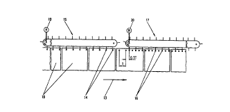
Figure 3 schematically shows the appliance according to the invention:
Not represented are separate transporting means unless the contact
elements are simultaneously used for transporting the panel 18. The plant
consists of two plant parts 15 and 17. The rotating clips and the continuously
cycled printed-circuit board panels 18 are shown. In case of a horizontal
continuous-cycle plant this is the top view. If thE~ panels are vertically
held,
this is a side view. As a matter of fact, also other configurations with
inclined
panels are possible. Arrow 13 shows the transporting unit. The contact
s
CA 02275261 1999-06-14
gripping points 14 of the first plant part 15 are represented as a circle. The
contact gripping points 16 of the second plant part 17 are represented as a
filled circle. The offset V of points 14 and 16 acxording to the invention on
the
printed-circuit board panel in this example definnes half a spacing T. In
general, the offset V = T, divided by the number of subsequently connected
plant parts. The defined offset of the contact gripping points is achieved by
the following measures: All plant parts lead to uniform distance of the
contact
gripping points through equal distance of the contact elements in transporting
direction. All plant parts produce at the same transporting and feeding
velocity for the contact elements. The distance T from one plant part to the
following plant part remains constant. Under these conditions, the individual
drives 19 and 20 in both plant parts run with phase synchronisation. The
distance of the contact gripping points 0,5 T corresponds to a phase shift of
180° which is permanently kept between both drives. It is safeguarded
by
synchronising the drives 19 and 20 with known means and methods of drive
engineering. With the same means and methods, the phase relations are
electrically adjusted.
Figure 4 shows how the plate thickness flow 21 is levelled by the defined
offset V of the contact gripping points 14 and 16. The plate thickness
minimum 10 is increased, the maximum 8 is reduced. The tolerance zone 6
represented as an example, however) is still e~;ceeded and/or fallen below.
Figure 5 shows the plate thickness flow 22 in three series connected
continuos-cycle plant parts. The contact gripping points of the first and
second plant part are again designated with 14. and 16 and those of the third
one with 23. In this example, the tolerance zone is not exceeded or fallen
below since owing to the more frequent changE~ of contact elements during
the transfer from one plant part to the next and owing to the exposure of the
9
CA 02275261 1999-06-14
former covered contact gripping points smaller variations occur. For this
reason, the points of the board and/or film surf<~ce that have previously been
used as contact gripping points can be metallised in subsequent plant parts.
Figure 6 shows the plate thickness flows 25, 2Ei and 27,28 resp. across the
transporting direction as they result from the processes according to Figures
4 and 5 resp. The representations can be compared with the representation
in Figure 2 as far as the scale is concerned. The position of the contact
gripping points on the printed-circuit board 18 i:; marked with the arrow 24.
The plate thickness flows 25 and 26 in both figures apply for the maximum 8
and for the minimum 10 in two series-connected plant parts. The flows 27
and 28 accordingly apply to three plant parts. T'he corresponding limits 29
and 30 for the usable range of the printed-circuit board panel 12 where the
achieved plate thicknesses still lie within the given tolerance range are
shown
in Figure 6.
If appropriately used, the process according to the invention and the
appliance can also be used for removing and/or thinning metals by
electrolytic etching. The measures to be used fir this purpose, deviate from
the above mentioned metallising process and from the appliance by the fact
that the polarity for the power supply to the contact elements and the panel,
on the one hand, as well as to the counter-electrodes (cathodes instead of
anodes), on the other hand, are reversed.
All the revealed features as well as combinations of the revealed features are
subject of this invention unless they are expressly designated as already
known.
1o
CA 02275261 1999-06-14
Reference list
1 Plate thickness flow in transporting direction with
processes according
to the state of the art
2 Location of a first contact gripping point (in first
plant part)
3 Location of a second contact gripping point (in second
plant part)
4 Position of the first contact gripping point
5 Position of the second contact gripping point
6 Tolerance zone
7 Plate thickness flow with maximum across the transporting
direction
with processes according to the state of the art
8 Plate thickness maximum between two contact gripping
points
9 Plate thickness flow with minimum across the transporting
direction with
processes according to the state of the art
10 Plate thickness minimum
11 Border to unusable panel edge
12 Edge of printed-circuit board panel, printed-circuit
film panel
13 Transporting direction
14 Contact gripping points of first plant part
15 First plant part
16 Contact gripping points of second plant part
17 Second plant part
18 Printed-circuit board, printed-circuit film panel
19 Drive in first plant part
20 Drive in second plant part
21 Plate thickness flow with two plant parts
22 Plate thickness flow with three plant parts
23 Contact gripping points of third plant part
24 Position of contact gripping points
25 Plate thickness flow with maximum for two plant parts
26 Plate thickness flow with minimum for two plant parts
m
CA 02275261 1999-06-14
27 Plate thickness flow with maximum for three plant parts
28 Plate thickness flow with minimum for three plant parts
29 Border for the usable area in case of two plant parts used
30 Border for the usable area in case of three plant parts used
12