Note: Descriptions are shown in the official language in which they were submitted.
CA 02275298 1999-06-15
-1-
Semiconductor component, in particular a solar cell,
and process for manufacture of same
The invention concerns a semiconductor component, in particular a solar cell,
with at least one semiconductor base material consisting of a mono or a
polycrystalline structure, which consists at least in part of pyrite with the
chemical
composition FeS2 and which is cleaned for the purpose of achieving a defined
degree of purity.
A number of generic semiconductor components or semiconductor photo-
components are already recognised which, given an efficiency level of
approximately 15%, are used commercially on the basis of the internal photo
effect of radiation energy from the sun or from light. Thin silicon or gallium
arsenide iron crystal with p and n conductive zones are used predominantly as
semiconductor materials.
Thin-layered solar cells are also recognised, in the case of which the
semiconductor layers are positioned on a carrier by means of metallization or
similar to produce a thickness in the range of micrometers (1 to 50 Vim).
Materials such as cadmium sulphide, cadmium telluride, copper sulphide or
similar are used for the semiconductor layers. These semiconauctor components
are only able to achieve an efficiency of 5 - 8%. However, they have a useful
power-weight ratio and are essentially more cost-effective to produce than
silicon-iron crystals.
According to Patent Specification EP-A 0 173 642, a generic solar cell is a
photo-
active pyrite layer with the chemical formula FeSz+,_x, which has a
concentration of
undesirable impurities of < 10z° per cm3 and a dopant of manganese (Mn)
or
arsenic (As) andlor cobalt (Co) or chlorine (CI). In practice, it would appear
that a
solar cell with this composition cannot achieve the required efficiency level.
In contrast, the object of this invention is to create a semiconductor
component, in
CA 02275298 1999-06-15
_2_
particular a solar cell on the basis of the type mentioned above which can be
used to achieve a higher efficiency than the known sun or light radiation.
Furthermore, the production costs in respect of this semiconductor component
will be sufficiently low that this type of solar cell would be suitable for
mass
production. A further object of the invention exists in using a semiconductor
material which can be disposed of easily an in an environmentally friendly
manner.
The invention is able to meet the objective in that the semiconductor base
material which consists at least in part of pyrite with the chemical
composition
FeS2, is combined or doped at least with boron and phosphorous respectively.
With a very advantageous type, the semiconductor base material is produced
from at least one layer of pyrite together with the elements boron and
phosphorous. Used in this way, an optimum and extremely efficient composition
is achieved, especially for solar cells.
These semiconductor components in accordance with the invention can be used
to produce solar cells which have a higher efficiency than any other known
solar
cells. The pyrite used as a semiconductor material has the advantage of being
a
natural material which can also be produced synthetically. The production
costs
can be kept to a level such that, given the increased level of efficiency,
profitable
use can be drawn.
Type examples of the invention and further advantages of same are explained in
more detail below with the aid of the drawing. This shows:
Fig. 1 a schematic cross-section through a semiconductor component in
accordance with the invention, shown on an enlarged scale,
Fig. 2 a schematic view of the energy split of the Fe d-conditions in
octahedral
and deformed octahedral ligand field of the pyrite
CA 02275298 1999-06-15
-3-
Fig.3 a schematic cross-section through a semiconductor component in
accordance with the invention with a heterojunction, shown on an
enlarged scale and
Fig.4 a schematic view of the energy bands with a heterojunction of a
semiconductor component in accordance with the invention.
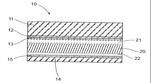
Fig. 1 is a schematic of a semiconductor component 10 in accordance with the
invention, which is formed in particular as a solar cell. In the type example
shown, this semiconductor component 10 has a multi-layered structure and may
for example, together with a number of adjacent cells, be clad in a metal
casing
formed as a panel, which is not shown in detail. The solar cell preferably has
a
cover plate from a transparent material, e.g. a layer of glass 11 or similar,
which
provides this cell with general protection against the effects of mechanical
forces,
such as impacts etc., against moisture andlor adverse weather conditions. A
laminate layer 12, from resin for example, together with an insulator 14
arranged
on the underside, e.g. as a ceramic plate, surrounds the solar cell, so that
the
inside of the solar cell is closed and therefore impervious to moisture, water
or
similar.
In accordance with the invention, the semiconductor base material 20 consists
of
pyrite or iron pyrite, which has a chemical composition of FeSz. The
semiconductor base material 20 is combined or doped with at least boron or
phosphorous, whereby in the example shown, the semiconductor base material
consists of a layer 20 of FeS2.
This semiconductor component 10 formed as a solid state cell consists of one
layer of the semiconductor base material 20 produced from pyrite, one layer of
phosphorous 21 and one layer of boron 22. This layer of phosphorous 21 and
this layer of boron 22 are applied to the corresponding surface of the layer
of
pyrite 20, in such a way that a bond within the sense of a dopant is produced
CA 02275298 1999-06-15
-4-
between the semiconductor base material and the phosphorous (P) respective
the boron (B). Preferably, these layers of phosphorous 21 and boron 22 are
applied in a very thin layer of several micrometers through a process
described
bel ow.
Thus, the required function of this semiconductor component 10 formed as a
solar cell is derived, from which, together with sunlight radiation, an
electric
current is produced, which is expediently tapped by the conductive materials
13
and 15 which are arranged above and below the semiconductor layers by a
recognised method, whereby the conductive material is protected by the
insulator
14. These conductive materials are connected to a consumer unit or similar by
means of cabling for which no diagrams are provided.
Fig. 1 is shown as a solar cell with a simple structure in accordance with the
invention. Clearly, both the conductive materials and also the semiconductor
layer can be provided in various configurations and in various quantities
This type of semiconductor component can be used as various types of solar
cell,
either for very small cells, e.g. calculators, or for solar cells for heating
houses
and large-scale plants, in which case they are used in particular to convert
solar
energy into electrical energy.
Pyrite and iron pyrite as natural rocks are the most widespread sulphides on
earth and these exist in Spain for example as a hydro-thermal ore area. The
individual pyrite crystals are either brass or mortar coloured with a high
degree of
hardness, i.e. approx. 6 to 6.5 on the Mohs' hardness scale. Pyrite has a
thermal
expansion coefficient at 90 to 300 K of 4.5x10-s K-' and at 300 to 500 K of
8.4x10⁻⁶
K'. The pyrite with a chemical composition of FeS2 has an elementary cell of
12
atoms and a unit cell length of approximately 5.4185 Angstrom units. The
typical
basic shape of the crystal habitus of the pyrite is a hexahedral, a cubic
shape, a
pentagonal dodecagon or an octahedron. A further advantage of this
semiconductor component is that this pyrite is extremely compatible with the
CA 02275298 1999-06-15
-5-
environment.
In terms of the efficiency of this solar cell 10 as described by the
invention, in
accordance with the general rules of quantum mechanics, only those photons,
the energy of which is at least equivalent to the width of the prohibited zone
and
no more than equivalent to the energy difference between the lower edge of the
valence band and the upper edge of the conduction band, are effective. The
quantity of resultant charge carriers is dependent not only on energy andV the
number of radiated photons per surface unit, but also on the absorption
coefficient a of the semiconductor. Compared with traditional semiconductor
materials, pyrite has a very high absorption coefficient, which, on the band
edge
with an absorption coefficient of a > 105 cm-', has a value of ~, < 1 fpm. By
creating
the semiconductor 10 in accordance with the invention, optimum use is made of
these pyrite properties.
In accordance with Fig. 2, the energy split of the Fe d-conditions can be seen
in
the octahedral O,, and deformed octahedral D3d ligand field of the pyrite. A
band
gap is created in the semiconductor base material by splitting the Fe d-
conditions
in occupied tz9 and unoccupied e9 conditions, whereby this band gap can be up
to
0.7 eV or more. The valence band has a width of 0.8 eV or more and the basic
group is separated by a gap, also of 0.8 eV. The conditions above the
conduction band are based on Fe 4s and 4p conditions. In the area of the
molecular orbital theory, the energy gaps in the case of pyrite are produced
by
splitting the 3d conditions of the iron in energetically lower occupied t29
and
unoccupied eg conditions. The split is caused by the octahedral ligand field
of the
sulphur, which is easily deformed and which leads to a further and in this
case
significant split in the energy level.
Fig. 3 on the other hand shows schematically a cross-section of a
semiconductor
component 50 in accordance with the invention, which is formed from at least
one
upper layer of pyrite 51, which forms the semiconductor base material 40, and
which consists of a layer of boron 52 and a layer of phosphorous 53. The
pyrite
CA 02275298 1999-06-15
-6-
51 is arranged on the upper side, which initially accepts the effects of the
sun
radiation or similar. With this arrangement of layers however, in accordance
with
the invention, a compound is formed with the adjacent basic pyrite material
51, or
the phosphorous 53 and the boron 52 are integrated into the adjacent basic
pyrite
material. The conductive elements can be arranged such that they come into
contact with the layers 51, 52, 53, for which no further details are given.
In contrast to the semiconductor base material 40 produced by layers as shown
in Fig. 3, one or more layers of boron and/or one or more layers of
phosphorous
can be arranged laterally in the pyrite target produced as a single crystal
for
example.
The semiconductor base materials 20 andlor 40 for these solar cells 10, 50 in
accordance with the invention can be produced by various methods. The pyrite
in the composition of FeSz can be obtained either as a natural material or
produced synthetically from iron and sulphur.
When using natural pyrite crystals as the semiconductor base material, this
pyrite, which has a net charge carrying concentration of approx. 10'5 cm-3,
must
be treated by a recognised multi-zone cleaning process, so that it achieves a
defined purity of 99.9%. Also, the compound or dopant materials, phosphorous
and boron respectively, should also achieve a purity of 99.9%, in order to be
able
to produce cells in accordance with the invention of the highest quality from
same.
Various methods can be used for the artificial production or synthesis of the
semiconductor base material pyrite, whereby the base material is also treated
by
a multi-zone cleaning process, in order to achieve the highest possible degree
of
purity from the chemical compound.
The production method is suitable for gaseous phase transport (CVT), for which
the temperature gradient for producing the iron-sulphur compound should be
CA 02275298 1999-06-15
_ 7 _
between 250° and 1200°C. If pyrite is used as a natural base
material, the
temperature on the cooler side may vary between 250° and 850°C.
As a
transport medium for feeding the sulphur to the iron, bromine (Br2 FeBr3) or
another material may be used.
Crystal synthesis may occur for example in a sodium poly-sulphate solution.
The
pyrite can be synthesised from the cleaned base elements, iron and sulphur,
both
at the standard temperature gradients between 250° and 1200°C
and also at a
gradient of 200° to 1400°C. The CVT methods offer improved
reproducibility
during production and absolute pure crystals can be achieved in this way.
For achieving large single-crystal pyrite pieces, the production method which
uses molten solution with tellurium, BrCl2, Na, SZ or similar materials, is
used.
Another production variant for pyrite exists in RF sputter. This occurs in a
sputter
unit, where a pyrite target is sputtered with an argon-sulphur-plasma. The
flow of
argon is usually between 0.1 and 300 mllmin and the sulphur is obtained by
vaporising elementary sulphur. During separation, the working pressure of 0.01
mbar or higher, or even lower is maintained. The Self-Bias DC Potential used
is
set at 0 to 400 volts. The substrate temperature is selected from the range of
80°
to 950°C. With this process, a poly-crystal structure can in principle
be produced.
To produce the semiconductor components in accordance with the invention as a
thin film, an incongruent material system can be used. The reactive sputter
produced from a target of pyrite, the MOCVD methods and spray pyrolysis are
suitable. Moreover, the method of thermal evaporation assisted by a conveying
system which transports small quantities of a powder compound to the hot
evaporation source, guarantees that the material, dependent upon the high
temperature, is almost completely vaporised. This type of vaporisation offers
the
benefit that influence can be exerted on both the stoichiometry and also a
potential doping, since for example, the dopant can be added directly to the
powder compound. If iron films are sulphurised, either purely thermally or
with
CA 02275298 1999-06-15
_ g _
the aid of plasma, it is possible to start from pure base materials.
The thickness of the active layer has a major influence on the efficiency of
the
solar cell. To estimate the efficiency and the required cell parameters,
appropriate boundary areas can be specified.
For doping or combining the semiconductor base material with phosphorous and
boron respectively, the preference is to use the latter in a mass percentage
of
106 to 20% of the base material. This depends on the required properties of
the
finished semiconductor component.
The semiconductor component in accordance with the invention may also be
produced as a so-called tandem cell. In this case, a dopant layer of pyrite
and
one further p and n layer from another semiconductor crystal such as silicon,
gallium arsenide or from another available material can create a combined
effect.
With this type of semiconductor component, maximum use can be made of the
spectrum, if these various semiconductor base materials were able to cover the
energy gap of between 1.0 and 1.8 eV.
In accordance with Fig. 4 and within the scope of this invention,
heterojunctions
between various semiconductor components can be used, as explained in detail
above in respect of the type variant shown in Fig. 3. The condition however,
is
that the lattice constants and the thermal expansion coefficients of the two
materials do not vary greatly. As an example, in accordance with the
invention, a
p-semiconductor 31 from pyrite can be combined with a n-conductive
semiconductor 32 from a different material. This heterojunction causes band
discontinuity which is used in an innovative manner to influence the charge
carrier transport. With the two separate semiconductor materials 31 and 32,
the
band gaps E~, the work function OS and the electron affinity x are different.
Specially developed epitaxial growth methods are recognised for producing
heterojunctions, which are also used in relation to the semiconductor base
CA 02275298 1999-06-15
_g_
material used in this invention. Both the molecular beam epitaxy (MBE) and the
gaseous epitaxy (MOCVD) exist in the form of gaseous deposition from metal-
organic compounds.
In the case of the thin film solar cell with a heterojunction, phosphorous and
boron are preferably integrated or doped, through an ion implantation, into
the
surface of the semiconductor base material pyrite, which occurs with the aid
of
particle accelerators. Thus, after ionisation, the dopant atoms are increased
to a
high level of energy and injected into the base material, where, after a
characteristic penetration depth, they are arrested and remain. With this
implantation process, the lattice of the semiconductor crystal sustains
considerable damage and it has to be regenerated by thermal treatment. Thus,
the implanted impurities diffuse and are simultaneously integrated into the
lattice.
Accordingly, compound profiles form from ion implantations and impurity
diffusions.
The molecular beam epitaxy (MBE) process is a special vapour deposition
method. The material is vaporised in hot cylinder-shaped pipes with a small
front
opening. The size of this opening and the vapour pressure created in the
furnace
by the heat determine the material transport for the target. An ultra-high
vacuum,
controlled by a mass analyser and a cooled shielding plate create very clean
crystal layers. The structure of these crystal layers can be controlled quasi-
online by so-called RHEED measurements {Reflected High Energy Electron
Difraction) and their layer thicknesses are created precisely by a temperature
regulation and quick sealing to a layer of atoms.
In the case of a multi-layer structure, the semi-conductor component may have
up
to a hundred layers. It would therefore be feasible for the semiconductor
component shown in Fig. 3 to be created from more than three different layers,
in
this way, several layers of pyrite and if appropriate, several layers from
boron
andlor phosphorous could be used.
CA 02275298 1999-06-15
- 10-
The semiconductor component used as pyrite- as described above - may be
created - within the scope of the invention - not only as a single or multi-
layer
solid matter solar cell, but also as a thin film solar cell, as a MIS solar
cell, a
photo-chemical cell or similar.
The semiconductor component in accordance with the invention is used to the
best advantage as a solar cell, because as such, it achieves an
extraordinarily
high degree of efficiency. Clearly, this semiconductor component may also be
used for other purposes, such as a diode, a transistor, thyristor or similar.
A semiconductor component in accordance with the invention could in theory
also
function, if a layer of pyrite and a compound with same were produced on the
basis of boron (B) or phosphorous (P).