Note: Descriptions are shown in the official language in which they were submitted.
CA 02275572 1999-06-18
WO 98/28688 PCT/SE97/01963
1
METHODS AND DEVICES RELATING TO CIRCUIT HOARD CONSTRUCTIONS
FIELD OF INVENTION
The present invention relater to a method of producing
circuitry that includes one or more customised integrated
circuits, primarily application specific integrated circuits,
ASIC. The method is mainly intended to enable parallel
production of circuit boards and software for customised
integrated circuits, although it is also suitable for
application in , the development and verification of the
customised integrated circuit per se.
The invention also relates to a method of verifying the
function of a customised integrated circuit.
The invention also pertains to a device for verifying the
function of a customised integrated circuit.
BACKGROUND OF THE INVENTION
It is known from Japanese Patent Publication JP-6291219 to
use a special module in the development of systems that
include ASCIs. The module stands apart from the system during
development work, and can thereby be constructed separately.
In addition to an ASIC, the module also includes matching and
interference-suppression circuits and a clock generator
placed on the same side of a circuit board as the ASIC, and a
processor which is placed on tine other side of said circuit
board. In series production, t;he module is replaced by an
ASIC, which is mounted directly onto a circuit board.
Patent Publication JP-7201937 teaches a capsule for
integrated circuits that allows signals to be measured within
an integrated circuit. The obje~~t of the capsule is to reduce
CA 02275572 1999-06-18
WO 98/28688 PCT/SE97/01963
2
test costs in the development of integrated circuits of the
ASIC kind, for instance.
SLTNl~lARY OF THE INVENTION
When practising the method taught by JP-6291219, it is
necessary to prototype a completely novel circuit board when
having found a system that functions satisfactorily. This
method of procedure is both time-consuming and expensive,
since a completely new circuit board must be produced in the
series production of the circuitry.
Although the solution described in publication JP-7201937
enables a specific, customised integrated circuit to be
measured,? it does not solve the problems that are associated
with the prototyping of software and circuit boards for a
customised integrated circuit.
Accordingly, one object of the present invention is to enable
the construction and testing of customised integrated
circuits directly on the circuit board that will later be
used in series-production, i.e. without requiring the use of
a special test board.
The present invention also aims at enabling the parallel
development of software for the customised integrated circuit
and f or the circuit board in general.
Another object of the invention is to provide an effective
prototype solution that allows a circuit board which includes
a customised integrated circuit to be tested in a virtual
environment prior to the fabrication of the customised
circuit.
CA 02275572 1999-06-18
WO 98/28688 PCT/SE97/01963
3
In addition, the invention enables the logic function of a
customised integrated circuit mounted on a circuit board to
be readily verified.
According to a third aspect, the present invention relates to
a method of prototyping circuitry for a circuit board. One or
more programmable logic elements and peripheral logic
required by said logic element or elements are mounted on the
rear side of a circuit board, i.e. on that side of the board
which normally carries no circuits or components. The
programmable logic circuit has the same logic function as
that which a customised integrated circuit that has still not
been produced is perceived to have. The connections of the
programmable logic circuit area passed through the circuit
board and connected to other board-mounted circuits and
components, in the same way as the customised circuit will be
connected. The entire system comprised of the circuit board
and its circuits and components is then tested. If the system
functions as desired, the programmable logic circuit is
removed and replaced by the cu:~tomised integrated circuit as
soon as the circuit become:> available. The customised
integrated circuit is mounted. in the same place as the
programmable logic circuit, but: on the opposite side of the
circuit board.
If, however, the system does not function as desired, the
software of the programmable: logic circuit and/or the
circuitry on the circuit board is/are modified. The function
is then tested and the system modified until the set
specifications are fulfilled.
The method is therewith characterised by the method steps set
forth in Claim 1.
CA 02275572 1999-06-18
WO 98/28688 PCT/SE97/01963
4
According to a second aspect, the invention relates to a
method of verifying the function of a customised integrated
circuit. A programmable logic circuit designed as a logic
analyser is mounted on the rear~side of a circuit board. The
programmable logic circuit is designed to measure and analyse
output signals from a customised integrated circuit mounted
on the front side of the circuit board, subsequent to having
delivered certain predetermined input signals to said
integrated circuit and having executed given software. The
programmable logic circuit is connected to the customised
integrated circuit, whereafter said predetermined input
signals are delivered .to this latter circuit. The output
signals of the customised integrated circuit are registered
and analysed with the aid of the programmable logic circuit.
A method according to this second aspect of the invention is
characterised by the steps set forth in Claim 8.
One embodiment of the proposed device for verifying the
function of a customised integrated circuit on a circuit
board includes a test unit and a logic analyser, which are
mutually connected by a connecting unit. The logic analyser
is comprised of a programmable logic circuit which is
designed to this end and which is connected to the customised
integrated circuit from the rear side, or secondary side, of
the circuit board.
The inventive device is characterised by the features set
forth in Claim 9.
The invention makes the production of new customised
integrated circuits more effective, by virtue of enabling one
and the same circuit board to be used for testing purposes
and f or mass-production. When only one circuit board need be
CA 02275572 1999-06-18
WO 98/28688 PCT/SE97/01963
~>
fabricated, the invention thus reduces the development costs
for the complete circuitry on t:he board.
The invention allows other circuit board circuits and
components to be tested in parallel with the development of
software for the customised integrated circuit, therewith
also enabling the time taken to develop the complete
circuitry to be shortened.
The present invention enable; a prototype circuit for an
integrated circuit to be created without needing to use a
special circuit board when testing the prototype circuit.
The invention also enables new functions to be added to an
existing customised integrated circuit by connecting-up a
programmable logic circuit immediately beneath the customised
integrated circuit, said programmable logic circuit
implementing said new function:>.
Because when practising the inventive methods, the requisite
test equipment is mounted so:Lely on the underside of the
circuit board, there will not be generated on the underside
of said circuit board during the testing phase solder pads
that will remain unused in the: mass-produced version of the
circuit board. This simplifies and makes more effective both
manual and mechanical inspect:ion of the finished circuit
board.
BRIEF DESCRIPTION OF THE DRAWIrdGS
Figure 1 illustrates a prototype circuit board with which a
logic circuit is used in a typ~.cal manner during the creation
of circuitry and software for a customised integrated
circuit.
CA 02275572 1999-06-18
WO 98/28688 PCT/SE97/01963
6
Figure 2 illustrates a circuit board intended for mass-
production and which has mounted thereon a customised
integrated circuit produced in accordance with the aforesaid
method.
Figure 3 illustrates a circuit board having a programmable
logic circuit mounted on the secondary surface thereof during
development work, in accordance with the invention.
Figure 4 illustrates a circuit board intended for mass-
production.
Figure 5 illustrates a circuit board with which a
programmable logic circuit is used to verify the function of
a customised integrated circuit in accordance with the
invention.
Figure 6 illustrates a circuit board which includes both a
programmable logic circuit and a customised integrated
circuit in accordance with the invention.
Figure 7 is a flowchart that illustrates the first inventive
method.
Figure 8 is a flowchart that illustrates the second inventive
method.
The invention will now be described in more detail with
reference to preferred embodiments thereof and also with
reference to the accompanying drawings.
DESCRIPTION OF PREFERRED EMBODIMENTS
Figure 1 illustrates a typical prototype circuit board 100
with which a programmable logic circuit 150 is utilised in
CA 02275572 1999-06-18
WO 98/28688 PCT/SE97/01963
7
creating circuitry and software for a customised integrated
circuit 250, this circuit being illustrated in Figure 2. The
prototype circuit board, or printed board assembly 100 must
have larger dimensions than the mass-produced circuit board
200, since the programmable logic circuit 150 is much larger
than the customised integrated circuit 250. Also mounted on
the circuit board 100 are other circuits 110, 120 and
components 130, 140. The programmable logic circuit 150 has a
logic function which is identical to the intended function of
the customised integrated circuit 250. The function of the
logic circuit 150 in relation t:o the remaining circuits 110,
120 and to the components :130, 140 can be tested by
installing test software in the programmable logic circuit
150 and applying input signa:Ls thereto. Appropriate test
equipment is connected to the logic circuit 150 for measuring
the output signals from the programmable logic circuit 150.
The software and circuitry is modified until they function
satisfactorily together with the programmable logic circuit
150. In exceptional cases, it may also be necessary to modify
the actual configuration of the logic circuit 150.
Subsequent to achieving circuitry and software for the
customised integrated circuit 250 that fulfil the
specifications set with respect thereto, a new circuit board
200 on which the customised integrated circuit 250 is mounted
is produced in accordance with aaid earlier known method. The
connections of the integrated circuit 250 with remaining
circuits 210, 220 and with components 230, 240 on the board
200 correspond to the connections used with the programmable
logic circuit 150 on the prototype circuit board 100 during
the prototype phase. Figure 2 illustrates a circuit board 200
for mass-production.
CA 02275572 1999-06-18
WO 98/28688 PCT/SE97/01963
8
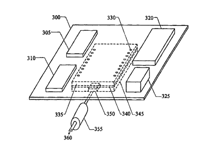
Figure 3 illustrates a circuit board 300 with which a
programmable logic circuit 345, for instance an FPGA circuit
(FPGA - Field Programmable Gate Array) has been mounted on
the secondary side of the board 300, in accordance with a
first embodiment of the invention. The programmable logic
circuit 345 is connected to circuits 305, 310 and to
components 320, 325 on the primary side of the board 300,
through the medium of through-penetrating holes 330. The
circuit 345 is connected to the circuit board 300 via a
compensating unit 340 and a mounting base 335. The
compensating unit 340 compensates for the extra conductor
length occurring between the programmable logic circuit 345
and the circuit board 300 in comparison with the case when a
customised integrated circuit is placed directly on the
primary side of the circuit board 300. An electrical contact
unit 350 connects the programmable logic circuit 345 to test
equipment 360, via a connecting unit 355.
Test software is installed in the programmable logic circuit
350 and input signals are applied thereto. The function of
the logic circuit 350 is tested in relation to the remaining
circuits 305, 310 on the circuit board 300 and in relation to
the components 320, 325 mounted thereon. The test equipment
registers the output signals from the programmable logic
circuit 350 and the output signals then analysed either
manually or mechanically. The software and circuitry are then
modified until they function satisfactorily together with the
programmable logic circuit 350. In exceptional cases, it may
also be necessary to modify the actual logic circuit 350.
Figure 4 illustrates mounting of a customised integrated
circuit board 430 on the primary side of the circuit board
400, subsequent to having achieved circuitry and software
CA 02275572 1999-06-18
WO 98/28688 PCT/SE97/01963
9
that fulfil the prescribed specifications. The customised
integrated circuit board 430 is connected to other circuits
410 , 420 and components 440, 450 in the same manner as that
used to connect the programmable logic circuit 345 during the
test phase.
Should the customised integrated circuit be found to contain
at least one function block which is known to be wrong,? a
programmable logic circuit is connected to the customised
integrated circuit on the secondary side of the circuit
board. Figure 5 illustrates a circuit board 500 on which a
customised integrated circuit 515 is assumed to have a faulty
function block 530. This function block 530 is blocked and
replaced with a corresponding, correct function block which
is implemented through functions in a first programmable
logic circuit 545. This circuit 545 is in contact with the
primary side of the circuit board, via a compensating unit
550, a mounting base 535, and through-penetrating holes 550.
Naturally, such a method assumes that the function block 530
of the customised integrated circuit 515 can be blocked by
some form of external influencE~. The international standard
Boundary-Scan Architecture and IEEE Std. 1149.1 disclose a
method by means of which function blocks in, e.g., an ASIC
can be isolated.
A circuit comprised of non-isolated function blocks in the
customised integrated circuit 515 and the first programmable
logic circuit 545 can then be tea ted in relation to remaining
circuits 505, 510 on the circuit board and components 520,
525 mounted thereon, by using a second programmable logic
circuit 555. This circuit 550 is connected to the customised
integrated circuit 515 and the first programmable logic
circuit 545 via the compensating unit 550 and the mounting
CA 02275572 1999-06-18
WO 98/28688 PCT/SE97/01963
base 535, and forwards measuring signals to test equipment
570, through an electrical contact 560 and a connection unit
565.
Figure 6 illustrates a circuit board 600 with which a
5 programmable logic circuit 640 is connected on the secondary
side of the circuit board 600. The logic circuit 640 is
designed as a logic analyser and is able to verify the
function of a customised integrated circuit 615 mounted on
the primary side of the circuit board 600.
10 The programmable logic circuit 640 is connected to the
customised integrated circuit 615 via a mounting base 635 and
through-penetrating holes 630. The programmable logic circuit
640 is also connected to external test equipment 655, via an
electrical contact unit 645 and a matching unit 650. The
measurement values obtained from the customised integrated
circuit 615 are registered in the test equipment 655 and
analysed, thereby enabling conclusions to be drawn with
respect to the function of the customised integrated circuit
615.
Figure 7 is a flowchart relating to a first embodiment of the
inventive method. The method results in a circuit board
intended for mass-production and including a customised
integrated circuit. In a first step 700, at least one
programmable logic circuit is mounted on the secondary side
of a printed board assembly, or circuit board, i.e. on that
side of the board on which no circuits or components are
normally mounted. In the last step 750 of the inventive
method, a customised integrated circuit is placed in position
in essentially the same manner although on the primary side
of the circuit board. Test equipment is connected to the
CA 02275572 1999-06-18
WO 98/28688 PCT/SE97/01963
1:1
programmable logic circuit in a second step 710 of the
inventive method. The followin<~ step 720 includes testing of
the function of the programmable circuit in relation to other
board-mounted circuits and components. If the function of the
programmable circuit is found to be satisfactory, in
accordance with step 730, there is mounted on the primary
side of the circuit board a customised integrated circuit
whose function, software and electrical connections coincide
with or are identical to those of the programmable logic
circuit. .
If, on the other hand, the function is not found to be
satisfactory, in accordance with step 730, the software,
circuitry and/or in exceptional cases also the function of
the programmable logic circuit: is modified. However, it is
normally desirable to avoid modifying the programmable logic
circuit, since a customised circuit having an identical
function is normally in the process of being manufactured on
this occasion.
Figure 8 is a flowchart relating to a second embodiment of
the inventive method. The purpose of this method is to verify
the function of a customised integrated circuit mounted on
the primary side of a circuit :board. Software is loaded into
the customised integrated circuit in a first method step 800.
In the next step 810, a programmable logic circuit designed
as a logic analyser is mounted. on the secondary side of the
circuit board. In the nexvt following step 820, the
programmable logic circuit is connected to the customised
integrated circuit through the circuit board. Input signals
are then delivered to the customised integrated circuit in
method step 830. Finally, the output signals from the
CA 02275572 1999-06-18
WO 98/28688 PCT/SE97/01963
12
customised integrated circuit are measured and analysed in
step 840, with the aid of the programmable logic circuit.