Note: Descriptions are shown in the official language in which they were submitted.
CA 02275589 1999-06-18
WO 98!28852 PCTISE97102121
DIGITAL CONTINUOUS PHASE MODULATION
FOR A DDS-DRIVEN PHASE LOCKED LOOP
S
BACKGROUND OF THE INVENTION
Technical Field of the Invention
The present invention relates generally to the radio transmitter field and, in
particular) to a digital continuous phase modulator for use with a direct
digital
synthesizer-driven phase locked loop.
Description of Related Art
The aim in developing new radio transmitters is to make them smaller and
cheaper to produce, while providing at least the same or better performance
than
prior transmitters. One way to achieve this goal is to move the digital domain
closer
1 S to the transmitter's output and thereby eliminate a number of analog
components.
Transmitters that employ a Direct Digital ;synthesizer (DDS) have been
developed
to achieve this goal. However, a problem that exists with the use of a DDS in
an
existing transmitter is that conventional modulation techniques used to
upconvert the
modulated intermediate frequency DDS signal to the radio frequency (RF)
transmit
band, are impractical for transmitters operating over wide frequency bands
because
of limitations imposed by the digital-to-analog converter (DAC) in the DDS.
Another problem exists with the use of a DDS-driven Phase Locked Loop
(PLL) in an existing transmitter, in that no effective modulation technique
has been
developed for such a device. For example) U.S. Patent No. 4,965,533 discloses
a
DDS-driven PLL, but with an unmodulat:ed synthesizer. A DDS with Gaussian
Minimum Shift Keying (GMSK) modulation is disclosed in U.S. Patent No.
5,425,055, but a DDS-driven PLL is not disclosed. Nevertheless, if DDS
technology is to be used in a communications system that employs fast
frequency
hopping and operates over relatively wide frequency bands (e. g. , cellular
system),
the use of a DDS-driven PLL topology will! be required in order for the
transmitter
to meet the stringent performance demands that will be placed on such a
system.
CA 02275589 1999-06-18
WO 98/28852 PCT/SE97/02121
-2-
SUMMARY OF THE INVENTION
It is an object of the present invention to provide a transmitter system with
a phase modulated DDS-driven PLL so that the frequency band of the DDS output
is significantly narrower than the frequency band of upconversion stages used
in
conventional transmitters. The PLL functions both as a narrow bandpass filter
and
a multiplier for the DDS signal.
It is another object of the present invention to provide a radio transmitter
in
which there are significantly less spurious emissions in the transmitted
signal than
in a conventional transmitter. The PLL functions as a narrow bandpass filter.
It is yet another object of the present invention to provide a radio
transmitter
that can transmit over a relatively wide frequency band. The PLL multiplies
the
DDS output bandwidth.
It is still another object of the present invention to provide a transmitter
with
a DDS-driven PLL in which it is possible to modulate a reference signal from
the
DDS, and at the same time, obtain the desired modulation index at the output
of the
PLL.
It is another object of the present invention to provide a radio transmitter
that
can perform fast frequency hopping, where the frequency hopping lock in time
depends on the loop bandwidth in the PLL.
It is still another object of the present invention to provide a radio
transmitter
that is smaller and cheaper to produce, while providing better performance
than
prior transmitters.
In accordance with the present invention, the foregoing and other objects are
achieved by a phase modulation generator that is used to modulate the output
signal
of a DDS. The phase-modulated DDS output drives a PLL, which is an
upconversion stage for a radio transmitter, with the modulated DDS signal as
the .
PLL's reference. Since the PLL functions as a frequency multiplier, the
frequency
band of the DDS output is significantly narrower than the frequency band of '
upconversion stages used in conventional transmitters, and there are
significantly
less spurious emissions in the transmitted signal (the PLL also functions as a
narrow
bandpass filter). However, a transmitter employing the present phase-modulated
CA 02275589 1999-06-18
WO 98/28852 PCT/SE97/02121
-3 -
DDS-driven PLL topology can still transmit over a relatively wide frequency
band.
BRIEF DESCRIPTION OF THE DRAWINGS
A more complete understanding of the method and apparatus of the present
invention may be had by reference to the following detailed description when
taken
in conjunction with the accompanying drawings wherein:
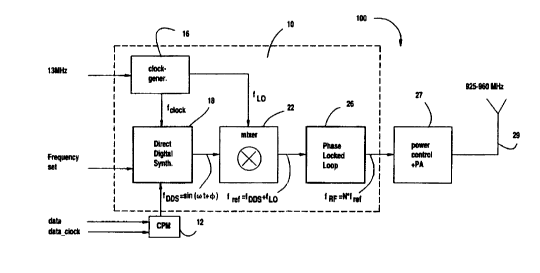
FIGURE 1 is a schematic block diagram of a system that illustrates the use
of a CPM generator with a DDS-driven PLL, and which can be used to implement
the apparatus and method of the present invention;
FIGURE 2 is a schematic block diagram of an exemplary DDS that can be
used to implement the apparatus and metr~od of the present invention;
FIGURE 3 is a schematic block diiagram of an exemplary PLL that can be
used to implement the apparatus and method of the present invention;
FIGURE 4 is a schematic block diagram of an exemplary CPM generator
that can be used to implement the apparanss and method of the present
invention;
FIGURE 5 is a schematic block diagram of an exemplary address calculator
that can be used to implement the apparatus and method of the present
invention;
FIGURE 6A is a diagram that illusvtrates the memory contents of a memory
section for a conventional GMSK DDS transmitter without a multiplying
upconversion stage.
FIGURE 6B is a diagram that illustrates the memory contents of memory
section 54 in FIGURE 4 for a DDS-driven PLL transmitter, in accordance with
the
present invention;
FIGURE 6C is a diagram that illustrates the phase states for the transmitter
of FIGURE 6A.
FIGURE 6D is a diagram that illustrates the phase states for the DDS-driven
PLL transmitter of FIGURE 6B.
FIGURE 7 is a schematic block diagram of an exemplary transmitter stage
that can be used to implement the apparatus and method of the present
invention;
and
CA 02275589 1999-06-18
WO 98/28852 PCT/SE97/0212~
-4-
FIGURE 8 is a diagram that illustrates certain signals generated by discrete
components in the continuous phase modulated, DDS-driven PLL systems shown in
,
FIGUREs 1 and 7.
DETAILED DESCRIPTION OF THE DRAWINGS
The preferred embodiment of the present invention and its advantages are
best understood by referring to FIGURES 1-8 of the drawings, like numerals
being
used for like and corresponding parts of the various drawings.
Essentially, in accordance with the present invention, a continuous phase
modulation (CPM) generator is used to modulate the output signal of a DDS .
The
phase-modulated DDS output drives a PLL, which functions as an upconversion
stage for a radio frequency transmitter, with the modulated DDS signal as the
PLL's
reference. Consequently, the frequency band of the DDS output is significantly
narrower than the frequency band of upconversion stages used in conventional
transmitters (e.g., without DDS-driven PLLs), and therefore, there are
significantly
less spurious emissions in the transmitted signal. Nevertheless, a transmitter
employing the present phase-modulated DDS-driven PLL topology can still
transmit
over a relatively wide frequency band. Additionally, by using a CPM generator
with a DDS-driven PLL in a transmitter, it is possible to modulate the (DDS)
reference signal with a smaller modulation index, h/N, and still obtain the
desired
modulation index, h, at the output of the PLL.
FIGURE 1 is a schematic block diagram of a system that illustrates the use
of a CPM generator with a DDS-driven PLL, and which can be used to implement
the apparatus and method of the present invention. In accordance with a
preferred
embodiment of the present invention, system 10 generally includes a CPM
generator
12, a DDS-driven PLL 14, and a clock generator 16. The data (e. g. , data or
speech
information) to be transmitted is converted by CPM generator 12 into a
continuous,
smoothly varying phase sequence, ~. The phase values in the sequence are
quantized on a phase modulation bus 13 and correspond to actual locations
between
-7t and ~ in the IQ plane. The phase of the converted signal will shift
between only
a limited number of phase states) which depends on the type of modulation
used.
CA 02275589 1999-06-18
WO 98/28852 PCT/SE97I02121
-S-
In this embodiment, a GMSK modulation scheme is used. How the phase of the
converted signal shifts between the different states is determined by a
mathematical
function. This mathematical function generates a limited number of phase
trajectories that are stored in a memory location (e.g., in a memory
associated with
CPM generator 12). Depending on the data being input to CPM generator 12, a
specific phase trajectory representing l:he input data is output on the phase
modulation bus 13 and coupled to an input of a DDS 18.
The DDS-driven PLL 14 multiplies she signal spectmm on its reference input
(from bus 13) with a division ratio, N. Consequently, the modulation signal
spectrum generated by the DDS stage ( 18 ) should be reduced by the same
factor.
As such, the number of phase states in the IQ plane are increased or scaled by
the
factor, N. So) the corresponding phase trajectories stored in the memory
associated
with DDS 18 are also scaled by the factor, N, which decreases the modulation
index, h, by the same factor (N).
DDS 18 modulates a first intermediate frequency signal, FDDS, with the phase
values input from bus 13. The signal, FDDS, can be readily altered by loading
a new
digital control word in a phase accumulator in DDS 18, which advantageously
enables a transmitter employing DDS-driven PLL 14 to effectuate fast frequency
hopping in very small increments (e.g., snnaller than 1Hz).
The output signal from DDS 18 is bandpass filtered in filter 20 and can be
mixed (as an option) by a mixer 22 with a local oscillator signal, fLO, from a
clock
generator 16. The signal output from mixer 22 is bandpass filtered in filter
24,
which passes one of the sidebands in the combined signal from mixer 22. The
signal
from bandpass filter 24 is used as the reference signal for the PLL stage 26
and
upconverted with (or multiplied by) the division ratio, N. This reference
signal
contains the "downscaled" modulation signal spectrum, which is also multiplied
by
the ratio, N.
The frequency of the output signall, SRF, from PLL stage 26 is within the
transmit frequency band, and can be expressed as:
SRF-~LO~'SDL~S) x N,
CA 02275589 1999-06-18
WO 98/Z8852 PCT/SE97/02121
-6-
where N is the division ratio in the PLL. For this embodiment, exemplary
values
used can be SpDS - I5.625-20.OOOMHz, fLO =100MHz, and N = 8) which results in
.
a transmit output frequency band of SRF = 925-960MHz (e. g. , Extended GSM
downlink band).
An important advantage of using system 10 and associated method as
illustrated by FIGURE 1 is that the frequency band at the output of DDS 18 can
be
kept narrow enough to exclude the harmonics. In other words, the higher
frequency
bound of the signal spectrum, SDps, can be less than twice its lower frequency
bound, within the same time period as the higher bound is substantially lower
than
the clock generator signal, f~,~k (which is important in order to be able to
exclude
harmonic aliases in the DDS output band). Another important advantage of using
system 10 and associated method is that any alteration of the modulation
signal
spectrum caused by the division ratio) N, can be corrected by the use of CPM
generator 12 as shown.
More precisely, in the preferred embodiment, clock generator 16 in system
10 generates a DDS clock signal, which is a harmonic of the system clock
signal and
functions to lock the DDS clock frequency to the system clock frequency.
Consequently, by making the DDS clock an integer multiple of the system clock,
the
hardware required for CPM generator 12 can be significantly reduced. Also, the
same clock signal (or another harmonic of the system clock) can be output from
clock generator 16 and used for the local oscillator frequency, fro, which can
be
mixed with the filtered DDS signal, SDDS, to upconvert the DDS signal.
FIGURE 2 is a schematic block diagram of an exemplary DDS (e.g., DDS
I8 in FIGURE 1), which can be used to implement the apparatus and method of
the
present invention. Specifically, a phase modulated signal, S, can be expressed
as:
'SDDS-KSIYl ~27LfDD~ +(~DDSO
where f represents the frequency of a signal, ~ represents the information to
be '
transmitted, and K is a constant. No amplitude information can be modulated on
the
resulting PLL output by the DDS reference signal. This makes the output a pure
phase modulated signal without any amplitude variations, which is a
significant
CA 02275589 1999-06-18
WO 98/28852 PCT/SE97/02121
advantage in comparing the present DDS-driven PLL transmitter with
conventional
transmitters employing an IQ modulator, or GMSK modulated DDS transmitters.
The phase sequence of an analog signal, fDI)s, is created in a phase
accumulator 30
(e.g., an unmodulated intermediate frequency signal). The frequency of fpDS
can be
digitally controlled by a canstant that represents a desired output signal
frequency.
In this embodiment, phase accumulator 3C1 is a modulo 2"' adder (where m is
the
phase accumulator's buswidth) that functions to calculate a linear phase ramp.
The
phase of the ramp signal can be incremented in steps of a frequency control
word
each time the adder is clocked (e. g. , at the DDS clock rate) . The signal at
the
output of phase accumulator 30 represents angles between 0 and 2n) and forms
the
first part (2~fDDSt) of the sine argument in Equation 2.
The modulation data, ~pDS, is added to the phase value from phase
accumulator 30 at adder 32 to form the argument of the sine function
(27LfDDSt+~DDS)~ The resulting phase value is used as an address for a memory
location in sine function table 34. The contents of an addressed memory
location
are output from sine function table 34 and ~;,oupled to a digital-to-analog
converter
(DAC) 36. As such, DDS 18 functions to implement Equation 2 using the phase
modulation information) ~, from CPM generator 12.
Returning to FIGURE 1, the DAC (?~6) in DDS 18 generates several replicas
of the fundamental signal being converted ) so it is preferable to filter the
output
signal from the DDS with bandpass filter :'0. Bandpass filter 20 also
functions to
reduce spurious frequency components in the DDS output signal.
Mixer 22 can be used (optionally) to convert the DDS output frequency band
to a higher frequency band) in order to maintain a low loop division ratio, N,
in the
PLL. Mixer 22 generates both an upper and lower sideband. For this embodiment,
use of the upper sideband is preferred in order to be able to keep the
division ratio
in the PLL as low as possible. Consequently, the signal output from mixer 22
is
bandpass filtered in filter 24, in order to select the upper sideband for
further
processing, and also suppress intermodulation products.
FIGURE 3 is a schematic block diagram of an exemplary PLL (e.g., PLL
26 in FIGURE 1), which can be used to implement the apparatus and method of
the
CA 02275589 1999-06-18
WO 98/28852 PCT/SE97/02121
_g_
present invention. Specifically, PLL 26 functions as a frequency multiplier,
which
multiplies the reference input signal, fret, bY the division ratio, N, and
produces a
high frequency signaI(e.g., RF signal), fo~" at its output. The output signal
from
PLL 26 is thereby locked to the reference input signal.
The output signal) f~,~, is generated by a voltage-controlled oscillator (VCO)
46, which is, in turn, controlled by the regulating loop of the PLL. The
control
voltage at the input of VCO 46 (from the output of loop filter 42) comprises a
lowpass-filtered version of the difference between the reference signal, f~ef,
and the
output signal) f~", divided by N (48). Consequently, the output signal from
PLL 26
is: f~,~=N*frcf. The lowpass loop filter (42) in the PLL suppresses unwanted
signals
close in frequency to the desired DDS reference) which is important in order
to be
able to meet the stringent requirements imposed on cellular systems.
A potential problem can occur if the reference signal, f~~r, is modulated,
because the modulation spectrum (bandwidth) will be expanded by the factor, N.
In order to compensate, the reference signal, f~ef, has a modulation index
that is
divided by N, so that the resulting modulation spectrum (bandwidth) output
from the
PLL has the original modulation index.
FIGURE 4 is a schematic block diagram of an exemplary CPM generator
(e. g. , digital CPM generator 12 in FIGURE 1 ), which can be used to
implement the
apparatus and method of the present invention. Essentially, CPM generator 12
functions to transform the incoming information (to be transmitted) to a
smooth,
changing phase sequence. The output signal from CPM generator 12 is coupled
via
the modulation bus 13 to the modulation input of DDS 18. Basically,
information
symbols are transmitted as changes in the phase of the transmitted carrier.
Since the
PLL (26) functions to multiply the signal spectrum appearing at its input, CPM
generator 12 takes this PLL function into account. The transition between the
phase
angles in the signal to be transmitted are predetermined by the history of
incoming
data, a function that depends on the modulation scheme used,
and the division ratio, N, of the PLL. The number of possible phase states on
the
output bus of the PLL is N times the number of states in the IQ plane of the
chosen
modulation scheme.
CA 02275589 1999-06-18
WO 98/28852 PCT/SE97/02121
-9-
The phase of the signal to be transmitted can be expressed as ~(t, a) and
represents the actual phase of the transmitter's output. This signal contains
the
information to be transmitted, which, in turn, depends on the data vector, a,
and the
time, t. Any phase modulated signal can be described by an expansion of
Equation
2, and expressed as:
SRF(t,a)= T sin(2.nft+~(t,a)),
where T is the symbol time (l/information rate), and E is the energy in one
symbol.
Since the energy, E, and symbol time, T, are constant, they can be understood
but
omitted from the following discussion. The data vector, ak, can comprise M
symbols (M is even). In a binary system, M=2, which means that the data
symbols
I 0 are + 1 and -1. The data vector can be expressed as:
akE~(1,3,5, ..., M-1?.
For this embodiment, the phase equation for a CPM scheme can be expressed
as:
~~t~a)=2~~~ akg~l-k~+~o~
The function, q(t), in Equation 5 represents the phase smoothing response (a
filter
function) that smooths out the resulting phase trajectory between two phase
states.
The expression, fro, represents the initial phase, which is preferably set to
zero. The
modulation index, h, and the PLL division ratio, N, determine how much the
phase
is allowed to change. The phase pulse is zero for t < 0, and constant for t >
LT)
where L is the correlation length (the length of the bit history taken into
account).
Accordingly, Equation 5 can be expanded and expressed as:
k-1
~(t~ak)=2'~Nak9~t-k~+2~~r-~t' a~q(t-iTj+8. (6)
CA 02275589 1999-06-18
WO 98/28852 PCT/SE97102121
-10-
The phase state depends on all data bits older than L, and changes in steps
of h~/N. The expression, 8, in Equation 6 is the state vector that represents
the .
phase state that is "updated" each symbol interval T. The phase state
described by
Equation 6 "remembers" the bit history and thus keeps the output phase (from
the '
CPM modulator) continuous. The phase state can be expressed as:
h k-L
8=~c-~ a..
N~=o
This part of the CPM phase equation has the greatest impact on the hardware
used to implement the CPM generator, when the PLL division ratio, N, is a
higher
number, since more phase trajectories have to be stored in memory. Notably,
for
this embodiment, an important consideration when calculating the phase
trajectories
is that they should be continuous at the ends of the interval, -~ to ~.
Consequently,
the summation in Equation 7 should be in modulo 27r and so implemented in the
CPM generator hardware.
Returning to FIGURE 4, an exemplary topology for a CPM generator is
shown. In this embodiment, CPM generator 12 includes an address calculator 52
1 S and a memory section 54. For example, memory section 54 can be a
programmable
read-only-memory (PROM). Address calculator 52 provides a capability of
implementing numerous CPM schemes with different correlation lengths (L) and
PLL division ratios (N). The incoming serial data is differentially enrr,rtP~
h.~
encoder 50 (as an option), and transformed to an address sequence by address
calculator 52. The resulting address sequence corresponds to a specific phase
trajectory stored in memory section 54. The phase trajectories corresponding
to the
addressed sequences are output on a phase data bus, with a rate equal to the
data clock signal multiplied by R. The expression, R, represents the number of
,
samples per phase trajectory.
The clock rate can be reduced with the integration factor, I, in order to save
memory space. The phase data rate is equal to the DDS clock rate/I prior to
reaching the optional integrator 56, and can be increased to the DDS clock
rate, by
multiplying it with I in integrator 56. Consequently, the phase data rate at
the CPM
CA 02275589 1999-06-18
WO 98/28852 PCT/SE97/02121
-1I-
generator output can be the same as the internal rate in the DDS. For this
embodiment, the optimal memory space used in memory section 54 is equal to
32NR/I words. This can be reduced further due to the symmetrical nature of the
trajectories, but it would, in that case, require more hardware in the address
calculator.
FIGURE 5 is a schematic block diagram of an exemplary address calculator
(e.g., address calculator 52 in FIGURE 4), which can be used to implement the
apparatus and method of the present invention. Address calculator 52 functions
to
calculate which phase trajectory corresponds to a specific combination of
incoming
data bits and their history. For this embodiment) address calculator 52
functions to
implement Equations 6 and 7 above. For example, the incoming data are shifted
into register 60. By inputting an L control word to multiplexer 62, the
correlation
length, L, of the incoming data bits can be adjusted to an appropriate length
by
controlling the number of bits that are shifted out of register 60. By
inputting an N-
I S control word to an up/down counter 64, the loop division ratio, N, can be
compensated for, also by controlling the number of bits shifted out of
register 60.
Additionally, by inputting a DDS clock/I control word to sample counter 66,
the
number of samples (R) made of the phase t~.-ajectory can be controlled. The
address
sequence calculated by address calculator _'i2 is input to memory section 54,
which
stores the corresponding phase trajectory that is output to the DDS (18).
FIGURE 6A is a diagram that illustrates the memory contents of a memory
section for a conventional GMSK DDS transmitter without a multiplying
upconversion stage. FIGURE 6B is a diagram that illustrates the memory
contents
(phase trajectory) of memory section 54 in FIGURE 4 for a DDS-driven PLL
transmitter) in accordance with the present uivention. FIGURE 6C is a diagram
that
illustrates the phase states for the transmitter of FIGURE 6A, and FIGURE 6D
is
a diagram that illustrates the phase states for the DDS-driven PLL transmitter
of
FIGURE 6B.
Referring to FIGUREs 6A and 6C) the diagrams show the memory contents
in a memory section and associated phase smtes, respectively, for a specific
solution
where GMSK is implemented with a PLI~,. division ratio of N =1 (e. g. ,
without
CA 02275589 1999-06-18
WO 98/28852 PCT/SE97/02121
-12-
compensating for the division ratio). FIGUREs 6B and 6D show the memory
contents of memory section 54 and associated phase states, respectively, for a
specific solution, but where GMSK is implemented with a PLL division ratio of
N = 8 and the division ratio is compensated for, in accordance with the
present
S invention.
For this embodiment, the CPM variant of GMSK has the following
parameters: (1) the phase smoothing response, q{t), is a Gaussian pulse; (2)
the
correlation length, L=3; and (3) the modulation index, h=0.5. The phase
smoothing response in Equations 5 and 6, along with the correlation length
(L),
modulation index (h), symbol time(T), and PLL division ratio (N) determine the
memory contents of an addressed location in memory section 54 (e.g., as shown
in
FIGUREs 6B and 6D).
FIGURE 7 is a schematic block diagram of an exemplary transmitter stage,
which can be used to implement the apparatus and method of the present
invention.
1 S Generally, the continuous phase modulated, DDS-driven PLL shown in and
described above with respect to FIGURE 1 can be used for the components
denoted
by numeral 10 in FIGURE 7. The RF output signal from PLL 26 is coupled to a
. power control and amplifier stage 27, and then transmitted from antenna 29.
As
shown in FIGURE 7, the continuous phase modulated, DDS-driven PLL and
transmitter output stage can be implemented in a cellular network radio
transmitter
(e.g., in either a base station or mobile station), or any transmitter that
uses a digital
modulation scheme.
FIGURE 8 is a diagram that illustrates certain signals generated by discrete
components in the continuous phase modulated, DDS-driven PLL systems shown in
FIGURES 1 and 7. In the preferred embodiment, as shown, the PLL division
ratio,
N, being used is 8, and the channel spacing in the DDS output being used is
about
25kHz, which will increase 8 times to about 200kHz after the PLL. As a
consequence of using the systems and methods illustrated by FIGUREs 1 and 7,
the
output signal spectrum, fpDS, from DDS 18 is about 4.375MHz wide. The output
3 0 sidebands from mixer 22 are also about 4.375MHz wide. The output spectrum
from
the PLL (26) is 8 times wider (about 35MHz). On the other hand, for a
CA 02275589 1999-06-18
WO 98/28852 PCT/SE97/02121
-13-
conventional system that does not use a continuous phase modulated, DDS-driven
PLL for an upconversion stage, the output spectrum of a DDS used in such a
system
would be about 35MHz wide. As such, the frequency band of the DDS output in
the present CPM DDS-driven PLL embodiment is significantly narrower than the
frequency band of upconversion stages used in conventional transmitters (e.g.,
without DDS-driven PLLs), and therefore, there are significantly less spurious
emissions in the transmitted signal. However, a transmitter employing the
present
phase-modulated DDS-driven PLL topology can still transmit over a relatively
wide
frequency band.
Although a preferred embodiment of the method and apparatus of the present
invention has been illustrated in the accompanying Drawings and described in
the
foregoing Detailed Description, it will be understood that the invention is
not limited
to the embodiments) disclosed, but is capable of numerous rearrangements,
modifications and substitutions without departing from the spirit of the
invention as
I S set forth and defined by the following claims.