Note: Descriptions are shown in the official language in which they were submitted.
CA 02275753 1999-06-22
_ WO 99/Z3722 PCT/US98/23432
COMPRESSION CONNECTOR
BACKGROUND OF THE INVENTION
1. Field of the Invention
This invention relates to electrical connectors
and, more particularly, to high density electrical
connectors utilized to electrically connect electronic
devices disposed on two or more printed circuit boards.
2. Description of the Prior AYt
Increased integration of electronic devices has
created an interconnection problem for printed circuit
boards receiving these devices. Specifically, the number
of interconnections required to electrically connect
together two or more printed circuit boards receiving these
electronic devices has exceeded the connection densities of
prior art pin-in-socket connectors. Moreover, these prior
art pin-in-socket connectors typically have relatively long
and unshielded lengths which have uncontrolled impedances
resulting in less than desired electrical performance.
A high contact density connector utilizable for
electrically connecting together electronic devices
received on two or more printed circuit boards and
overcoming the foregoing problems is disclosed in an
article entitled "A High Density Edge Connector" by J.
Campbell et al., Copyright 1995 IEEE. This article
discloses a flex circuit formed of a 2 mil thick polyimide
film having 3 mil wide copper lines plated onto one side
thereof and 25 mil round contact pads plated on the side of
the film opposite the circuit lines and along both edges of
the film. "4 mil diameter plated through-holes, or vias,
extend between the contact pads on one side of the film and
the circuit lines on the other side. Palladium dendrites,
or spires, are electro-deposited on surfaces of each
contact pad. These dendrites straddle dust or fibers and
puncture oils or films present on each contact pad prior to
connector mating and produce on each contact pad a
multitude of conductive connections. The connector
includes a molded plastic force block to which elastomeric
cylinders are molded. These cylinders act as springs which
provide force, when compressed during assembly, to make and
CA 02275753 1999-06-22
_. WO 99/23722 PCTNS98/23432
maintain an electrical connection between the contact pads
on the film and the pads on a printed circuit board. One
cylinder is provided for each contact and compensates for
any variation in planarity and tolerance accumulation.
Conical alignment pins are utilized to mate alignment holes
in the flex circuit with alignment holes in the printed
circuit board during assembly, thereby ensuring proper
registration between the contact pads on the film and the
pads on the printed circuit board.
l0 Another flexible circuit connector for connecting
a daughter card and a mother board is disclosed in an
article entitled "A High Density Pad-On-Pad Connector
Utilizing A Flexible Circuit« by R.S. Pokrzywa, Copyright
1993 IEEE. This connector utilizes a two-sided flex
circuit having plated, spherical contacts contacting flat
printed circuit pads on the daughter card and on the mother
board. The spherical contacts on the flex circuit are 5
mils in diameter and have a copper base metal overplated
with nickel and gold. Alignment pins are utilized to align
the flex circuit, the daughter card and the mother board so
that each spherical contact mates with a desired printed
circuit pad. Precipitation hardened stainless steel curved
beams provide contact force for reliable connection between
the spherical contacts and the printed circuit pads.
During actuation, the curved beam is flattened to produce
a uniform load across the contact area. An elastomeric pad
is positioned between the beam and the contact area to
accommodate local discrepancies in load across the contact
area and to focus the connector forces. In, one embodiment,
the elastomeric pad has a plurality of elastomeric
cylinders utilized to back-up the spherical contacts. In
another embodiment, where size does not permit molding
individual cylinders for each spherical contact, an
elastomeric rib is utilized to back a row of spherical
contacts.
A problem with spherical contact pads and
electro-deposited dendrites on contact pads is that they
- 2 -
CA 02275753 1999-06-22
WO 99/23722 PCT/US98/23432
inconsistently break through contaminants, such as oxides,
films or foreign materials, that may be present thereon or
on the contact pad of a printed circuit board. Hence,
inadequate electrical contact or, in some instances, no
electrical contact is made between the contact pad of the
flexible circuit and the contact pad of the printed circuit
board. Moreover, the formation of dendrites on the
contacts of the flexible circuit increases the cost of such
connectors.
It is therefore an abject the present invention
to provide a connector which overcomes these drawbacks of
the prior art connectors. It is an object of the present
invention to provide a compression connector contact that
promotes electrical contact with a conductive pad of a
printed circuit board. It is an object of the present
invention to provide a method for making a connector that
utilizes the provided compression connector contact. It is
an object of the present invention to provide a method of
making a flexible circuit connector that is less costly to
manufacture than the prior art flex circuit connectors.
SUMMARY OF THE INVENTION
Accordingly, we have invented a compression
connector utilized to electrically connect together
conductive pads disposed on one or more substrates. The
compression connector includes a flexible substrate having
a plurality of conductive through-holes therein and at
least one conductive line thereon extending between at
least two of the conductive through-holes. The compression
connector also includes a plurality of contacts. Each
contact has a post connected to a base of a crown-shaped
head having a plurality of projections around the periphery
of the base that extend away from the base in a direction
opposite the post. The post of each contact is secured in
one of the plurality of conductive through-holes.
A compression mat can be positioned on the side
of the flexible substrate opposite the crown-shaped heads
of the plurality of contacts. The compression mat can
- 3 -
*rB
CA 02275753 1999-06-22
WO 99/23722 PCT/US98/23432
include a plurality of resilient cylinders extending away
from a resilient base. Each resilient cylinder can have a
distal end alignable in registration with a distal end of
the post of one of the plurality of contacts secured in one
of the plurality of conductive through-holes.
A transfer film can be utilized to transfer the
plurality of contacts to the flexible substrate prior to
securing each post in one of the plurality of conductive
through-holes. The transfer film preferably has a
plurality of elastically deformable receiving apertures
which receive and secure the crown-shaped heads of the
plurality of contacts.
The compression connector can also include a
rigid substrate, such as a printed circuit board, which has
a plurality of the conductive pads on a surface thereof and
at least one conductive line connected to at least one of
the conductive pads. The rigid substrate and the flexible
substrate are alignable so that at least one projection of
each contact on the flexible substrate is aligned in
registration with one of the conductive pads on the surface
of the rigid substrate.
A compression fitting can be positionable
adjacent the resilient base of the compression mat. The
compression fitting forces together at least one projection
of each contact and the conductive pad in registration
therewith. Each resilient column of the compression mat
contacts the distal end of a post of a contact and
functions as the spring when compressed to make and
maintain good electrical connection between the projection
and the conductive pad.
Preferably, a plurality of alignment holes in
each of the flexible substrate, the rigid substrate and the
compression fitting co-act with a like plurality of
alignment pins to align the flexible substrate, the rigid
substrate and the compression fitting so that the heads of
the plurality of contacts are in registration with the
plurality of contact pads. Each alignment pin is
- 4 -
CA 02275753 1999-06-22
_ WO 99/23722 PCT/US98n343I - -
preferably a bolt having a threaded end adapted to mate
with a threaded nut.
We have invented a compression connector contact
that includes a crown-shaped head having a base and a
plurality of projections disposed around the periphery of
the base and extending to one side thereof. A post extends
from the side of the base opposite the projections.
The side of the base opposite the post can have
a cavity formed therein in registration with a lengthwise
axis of the post. The base can have a periphery having a
generally rectangular outline. Each corner of the
generally rectangular outline of the base can be rounded
and can include one of the plurality of projections. Each
projection can have a rounded edge formed continuous with
the periphery of the base.
We have also invented a method of making a
connector that includes providing a plurality of contacts,
each contact having a post connected to a base of a crown-
shaped head. Each crown-shaped head has a plurality of
projections around the periphery of the base that extends
away from the base in a direction opposite the post. The
crown-shaped heads of the plurality of contacts are
inserted into a plurality of receiving apertures in a
transfer film so that the posts extend out of the plurality
of receiving apertures. A flexible substrate is provided
having a plurality of conductive through-holes therein and
a plurality of conductive lines thereon. At least one
conductive line extends between and electrically connects
at least two of the conductive through-holes. The transfer
film and the flexible substrate are mated so that the posts
of the plurality of contacts are received in the plurality
of conductive through-holes in the flexible substrate. The
posts of the plurality of contacts are fused to the
plurality of conductive through-holes in the flexible
substrate. The transfer film is then separated from the
flexible substrate and the plurality of contacts.
- 5 -
CA 02275753 1999-06-22
WO 99/23722 PCT/US98/23432
The plurality of contacts are formed from a
strip of conductive material. Each contact is connected to
an adjacent contact by a rib formed from the conductive
strip. Each contact is excised from its connecting rib and
inserted into one of the receiving apertures in the
transfer film. Each receiving aperture elastically deforms
to receive and retain the head of the contact therein.
BRIEF DESCRIPTION OF THE DRAWINGS
Fig. la is a cross section of a compression
connector in accordance with the present invention;
Fig. lb is an enlarged view of a portion of Fig.
la within line lb;
Fig. 2a is a plan view of a compression mat of
the compression connector in Fig. 1;
Fig. 2b is a side view of the compression mat of
Fig. 2a;
Fig: 3a is a plan view of a flexible substrate
used in the compression connector of Fig. 1;
Fig. 3b is an enlarged view of a portion of Fig.
3a within line 3b;
Fig. 4a is a plan view of a conductive strip that
has been formed to include a plurality of contacts that are
utilized in the compression connector of Fig. 1;
Fig. 4b is an enlarged view of a portion of the
conductive strip of Fig. 4a within line 4b;
Fig. 4c is a cross section taken along lines 4c-
4c in Fig. 4b;
Fig. 5 is a plan view of the conductive strip of
Fig. 4a aligned With a transfer film;
Fig. 6 is a cross section of the aligned
conductive strip and transfer film of Fig. 5 positioned
between a transfer base and an excising tool;
Fig. 7 is a cross section of the contacts of the
conductive strip of Fig. 4a received in receiving apertures
of the transfer film of Fig. 6 and positioned in alignment
with through-holes formed in the flexible substrate of Fig.
3a;
- 6 -
CA 02275753 1999-06-22
WO 99/23722 PCT/US98/23432
Fig. 8 is.a cross section similar to Fig. 7
showing the transfer film and flexible substrate mated
together with the posts of the contacts received within and
soldered to the through-holes of the flexible substrate;
and
Fig. 9 is a cross section similar to Figs. 7 and
8 and showing the separation of the transfer film from the
flexible substrate and contacts.
DESCRIPTION OF THE PREFERRED EMBODIMENT
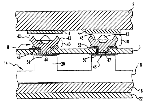
Referring to Figs . la-lb, a rigid substrate 2 ,
such as a printed circuit board formed of FR-4 or ceramic,
has a plurality of conductive pads 4 formed thereon in a
manner known in the art. The rigid substrate 2 may include
one or more conductive lines that extend between one or
more of the conductive pads 4 or between a conductive pad
4 and an electronic device connected to the rigid substrate
2. The conductive lines and electronic device are not
shown on the rigid substrate 2 in Figs. 1a-ib for
simplicity of illustration.
A flexible insulating substrate 6 having a
plurality of contacts 8 secured thereon is positioned
adjacent the rigid substrate 2. The flexible substrate 6
is preferably formed of a polyimide film such as Kapton~.
Kaptori is a registered trademark of E.I. DuPont DeNemours
& Company. The contacts 8 are secured on the flexible
substrate 6 in a pattern matching the pattern of the
conductive pads 4 on the rigid substrate 2. Each contact
8 includes a head 10 that extends away from a surface of
the flexible substrate 6. Aligning the flexible substrate
6 and the rigid substrate 2 positions the heads 10 in
registration with the conductive pads 4.
A compression fitting 12 is positioned on the
side of the flexible substrate 6 opposite the heads l0 of
the contacts 8. The compression fitting 12 includes a
compression mat 14 received in an aperture 15 of an
alignment sleeve 16. As shown in Figs. 2a-2b, the
compression mat 14 includes a resilient base 18, preferably
CA 02275753 1999-06-22
- WO 99/23722 PCT/US98/23432 -
having a generally rectangular outline, and a plurality of
resilient cylinders 20 extending from the resilient base
18. The compression mat 14 and the flexible substrate 6
are positioned so that distal ends of the resilient
cylinders 20 are aligned in registration with the contacts
8 on a surface of the flexible substrate 6 opposite the
heads 10. The compression fitting 12 includes a washer 22
positioned on a side of the alignment sleeve 16 adjacent
the resilient base 18 of the compression mat 14.
Preferably, the compression mat 14 is formed of a thermal
silicon rubber, the alignment sleeve 16 is formed from a
polyphenylene sulfide, UL 94 V-0, and the washer 22 is
formed from stainless steel.
The compression fitting 12, the flexible
substrate 6 and the rigid substrate 2 each have a plurality
of alignment apertures 24, 26 and 28, respectively. Each
alignment aperture 24, 26 and 28 is adapted to receive a
shaft of an alignment pin 30, such as a bolt having an
externally threaded end 31 adapted to mate with internal
threads of a nut 32. Applying the nuts 32 to the alignment
pins 30 urges together the compression fitting 12 and the
rigid substrate 2. This urging together forces into
contact the conductive pads 4 and the heads 10 in
registration therewith, and the distal ends of the
resilient cylinders 20 in registration with contacts 8 on
the surface of the flexible substrate 6 opposite the heads
l0. Continued application of the nuts 32 to the alignment
pins 30 compresses the compression mat 14 between the
flexible substrate 6 and the washer 22. This compression
causes the resilient cylinders 20 to deform against the
contacts 8 on the side of the flexible substrate 6 opposite
the heads 10. This deformation causes each resilient
cylinder 20 to apply a spring force between the head 10 and
the conductive pad 4 in registration therewith. This
spring force promotes between the head 10 and the
conductive pad 4 in registration therewith the formation
and maintenance of good electrical contact and compensates
_ g _
CA 02275753 1999-06-22
_ WO 99/Z3722 PCT/US98/23432 -
for any variations in planarity and tolerance accumulation.
Preferably, double-sided tape 34 is utilized to adhere
together adjacent surface of flexible substrate 6 and the
sides of the alignment sleeve 16.
The head 10 of each contact 8 has a base 40 and
a plurality of projections 42 disposed around a periphery
43 of the base 40. The projections 42 extend to one side
of the base 40 and give the head 10 a crown-shaped
appearance. Each contact 8 also has a post 44 that extends
l0 from a central part of the base 40 opposite the projections
42. A cavity 46 is preferably formed in each base 40
opposite the post 44 and in alignment with a lengthwise
axis 47 of the post 44.
With reference to Figs. 3a-3b and with ongoing
reference to Figs. la-ib, the flexible substrate 6 has a
plurality of through-holes 48 formed therein that are
adapted to receive the posts 44 of the contacts 8. The
wall of each through-hole 48 includes metallization 50
formed therein to form a conductive through-hole. The
metallization 50 in each through-hole 48 is preferably
connected to a conductive line 52 or to one or more
conductive ground planes 53 formed on the flexible
substrate b. The one or more conductive ground planes 53
are formed on one or both surfaces of the flexible
substrate 6 to reduce or eliminate cross-talk between
conductive lines 52 and/or to reduce or eliminate the
effect on one or more of the conductive lines 52 of
electro-magnetic interference from external sources. The
metallization 50 in each through-hole 48, the conductive
lines 52 and the conductive ground planes 53 are formed on
the flexible substrate 6 in a manner known in the art. To
maintain the post 44 of each contact 8 received in a
through-hole 48, the metallization 50 of each through-hole
48 and the posts 44 of the contacts 8 received therein are
fused together, preferably utilizing a solder 54.
With reference to Figs. 4a-4c, an array of
contacts 8 is formed by exposing a thin, flat strip 60 of
_ g -
CA 02275753 1999-06-22
WO 99/23722 PCT/US98/23432
conductive material to a stamping operation. The stamping
operation also forms from the strip 60 a plurality of ribs
62 that extend between and secure together adjacent
contacts 8.
In a preferred embodiment, the periphery 43 of
the base 40 of each head 10 has a generally rectangular
outline. Each corner 66 of the generally rectangular
outline of the base 40 is rounded and includes one of the
projections 42. Each projection 42 has a rounded edge 68
formed continuous with the periphery 43 of the base 40.
With reference to Fig. 5, to install the
contacts 8 in the flexible substrate 6, the contacts 8 are
first transferred to a flexible transfer film 70, such as
Kaptori . More specifically, the strip 60 having the array
of contacts 8 formed therein is aligned with the transfer
film 70 so that each contact 8 is aligned in registration
with one of a plurality of receiving apertures 72 in the
transfer film 70.
As shown in Fig. 6, the transfer film 70 is
positioned between the strip 60 and a transfer base 76 so
that the posts 44 of the contacts 8 are positioned in
opposition with the transfer base 76 through the receiving
apertures 72 of the transfer film 70. An excising tool 78
having a plurality of blades 80 and a plurality of push
pins 82 is positioned on a side of the conductive strip 60
opposite the transfer film 70. In use, the excising tool
78 is moved towards the base 76 so that the blades 80
excise the contacts 8 from the ribs 62. The excised
contacts 8 are then inserted into the receiving apertures
72 by the push pins 82 so that the lengthwise axes 47 of
the posts 44 are substantially coaxial with lengthwise axes
83 of the receiving apertures 72.
Before inserting the contacts 8, each receiving
aperture 72 has a diameter 84 that is less than a diagonal
distance 86 (shown in Fig. 4c) between opposite corners 66
of the base 40. As shown in Fig. 7, the receiving
apertures 72 elastically deform to receive and secure the
- 10 -
CA 02275753 1999-06-22
WO 99/Z3722 PCT/US98/23432
heads 10 of the contacts 8 therein. Preferably, each head
has a height 88 (shown in Fig. 4c) that is greater than
a thickness 90 of the transfer film 70. Hence, when the
heads 10 are inserted in the receiving apertures 72, the
5 posts 44 of the contacts 8 are preferably positioned
outside the receiving apertures 72. When the heads 10 are
received in the receiving apertures 72, the transfer film
70 and the flexible substrate 6 are positioned so that the
posts 44 are in registration with and receivable in the
10 through-holes 48.
As shown in Fig. 8, the flexible substrate 6 and
the transfer film 70 are brought together so that the posts
44 are received within the metallization 50 of the through-
holes 48. The contacts 8 are secured to the flexible
substrate 6 by fusing the posts 44 and the metallization 50
of the through-holes 48 together with the solder 54.
As shown in Fig. 9, the flexibility of the
transfer film 70 and the elastic deformability of the
receiving apertures 72 enables the transfer film 70 to be
separated, e.g., peeled away, from the contacts 8 secured
to the flexible substrate 6. When the transfer film 70 is
separated, the flexible substrate 6 and contacts 8 can be
utilized in the manner described above in connection with
Figs. la-lb.
As shown in Fig. 3a, a first plurality 96 of
through-holes 48 and a'second plurality 98 of through-holes
48 are preferably disposed on opposite sides of the
flexible substrate 6. When the contacts 8 are fused into
the first and second plurality 96, 98 of through-holes 48,
the side of the flexible substrate 6 adjacent the first
plurality 96 of through-holes 48 can be utilized to connect
to one rigid substrate (not shown) and the side of the
flexible substrate 6 adjacent the second plurality 98 of
through-holes 48 can be utilized to connect to another
rigid substrate (not shown) thereby effecting electrical
connection between the rigid substrates.
- 11 =
CA 02275753 1999-06-22
_ WO 99/23722 PCT/US98/23432
In a preferred embodiment, each post 44 has a
diameter between 7 and 8 mils and a length of 2 mils. The
head 10 of each contact 8 has a height of l0 mils and the
cavity 46 has a depth of 3 mils. The height of each
projection 42 is 4 mils and a distance 94 (shown in Fig. 9)
between rounded edges 68 of projections 42 on diagonally
opposite corner 66 is 21.5 mils. The strip 60 and contacts
8 are formed from a strip of 1/4 hard brass. The contacts
8 are plated with 5 micro-inches of soft gold over 30
micro-inches of palladium nickel over 50 micro-inches of
sulfamate nickel. The conductors 52 and the ground planes
53 of the flexible substrate 6 are formed from 1/2 ounce
copper which is deposited as a sheet on the flexible
substrate 6 and then patterned and etched utilizing
photolithographic and etching techniques known in the art.
Based on the foregoing, it can be seen that the
contacts 8 are sufficiently small so that manual
manipulation of contacts 8 into the through-holes 48 of the
flexible substrate 6 is not practical. To this end, and in
accordance with the present invention, forming the array of
contacts 8 from the strip 60 enables the contacts 8 to be
manipulated as an array. Similarly, the transfer film 70
enables the contacts 8 to be transferred as an array from
the strip 60 to the flexible substrate 6. The transfer
film 70 also helps maintain the posts 44 of the contacts 8
in the through-holes 48 during fusing of the posts 44 to
the metallization 50 of the through-holes 48. Hence, the
contacts 8 are manipulated as an array from the time they
are formed from the strip 60 in the stamping operation
until they are fused into the conductive through-holes in
the flexible substrate 6. This manipulation of the
contacts 8 as an array enables the compression connector of
the present invention to be manufactured efficiently and
cost effectively. Moreover, the compression connector of
the present invention avoids the prior art teaching of
plating contacts on the flexible substrate.
- 12 -
CA 02275753 1999-06-22
_ WO 99/23722 PCT/US98/23432 -
Because the metallization 50 in the through-holes
48 and the conductive lines 52 are pre-formed on the
flexible substrate 6, it is preferable to avoid soldering
the contacts 8 to the through-holes 48 prior to excising
the contacts from the ribs 62 due to concerns over cutting
with the blades 80 of the excising tool 78 the conductive
lines 52 or the metallization 50 in the through-holes 48.
Hence, the contacts 8 are first transferred to the flexible
transfer film 70 which is utilized to transfer the contacts
8 to the flexible substrate 6 and which may thereafter be
disposed as justified by the condition thereof.
The contacts 8 of the present invention are
believed to provide over prior contacts improved contact
with contact pads 4 on the rigid substrate 2.
Specifically, the rounded edge 68 of each projection 42
contacting one of the contact pads 4 cuts through oils or
films that may be present on the conductive pad 4 and/or
the contact 8 prior to mating, thereby enabling conductive
paths to be formed between each projection 42 in contact
with the conductive pad 4.
As can be seen from the foregoing, the present
invention provides a compression connector contact that
promotes electrical contact with a conductive pad of a
printed circuit board. The present invention also provides
a method for making a flexible circuit connector that
utilizes the provided compression connector contact and is
less costly to manufacture than the prior art flexible
circuit connectors.
The invention has been described with reference
to the preferred embodiment. Obvious modifications and
alterations will occur to others upon reading and
understanding the preceding specification. It is intended
that the invention be construed as including all such
modifications and alterations insofar as they come within
the scope of the appended claims or the equivalents
thereof.
- 13 -