Note: Descriptions are shown in the official language in which they were submitted.
CA 02275842 1999-06-21
Zhou 3
METHOD AND APPARATUS FOR ADJUSTING PILOT SIGNAL
RELATIVE TO INPUT SIGNAL
BACKGROUND OF THE INVENTION
1. Field of The Invention
This invention relates to radio frequency (RF) amplifiers and, more
particularly, to a pilot and input signal synchronization scheme for feed-
forward RF
amplifiers.
2. Description of Related Art
1tF amplifiers often add undesired distortion to an input signal, creating an
output RF signal on a main path comprising an amplified input signal and
distortion,
a significant component of which is intermodulation distortion (1MD). The
distortion
includes any undesired signals added to or affecting adversely the amplified
input
signal. IIVVIDs of a signal arises from intermodulation of the frequency
components in
the signal by each other in a nonlinear system, producing waves having
frequencies,
among others, equal to the sums and differences of the frequency components of
the
original signal. Feed-forward correction is routinely deployed in modern RF
amplifiers to reduce the distortion produced from the RF amplifier on the main
signal
2o path. The essence of the feed-forward correction is to isolate the
distortion produced
from the amplifier on a correction path so that at the final summing point,
the
distortion on the correction path cancels out the distortion of the RF signal
on the
main path.
Due to the unpredictability of input RF carrier pattern as well as the
resultant
location of the distortion, a known frequency component, i.e. the pilot, is
injected in
the main loop to mimic the distortion produced by the amplification process.
In feed-
forward amplifiers, the correction circuitry isolates the amplified pilbt
signal along
with the distortion onto the correction path and manipulates the pilot signal
and the
distortion on the correction path to combine with and reduce the pilot and the
3o distortion on the main signal path. The correction circuitry detects the
pilot signal
CA 02275842 1999-06-21
Zhou 3 2
and attempts to cancel the pilot signal from the main signal path. In
cancelling the
pilot signal from the main signal path, the correction circuitry cancels the
distortion.
There are two general types of pilot signals: continuous wave (CW) and
spread spectrum (SS) pilot signals. The CW pilot is easy to detect and
measure, but
runs the risk of being overlaid by one of the input carriers. Therefore, it is
advantageous to move the CW pilot outside of the band of operation. Otherwise,
the
pilot frequency should be constantly updated to find a quiet location in-band
where
there is no input Garners. For example, FIG. 1 shows the frequency response of
an
RF amplifier including the location of a CW pilot signal. The pilot signal can
be near
1o the lower edge of the operating band (e.g., pilot 1) or located near the
upper edge of
the band of operation (e.g., pilot 2). The pilot is positioned a spectral
distance of
0 f from an edge of the band of operation whose center frequency is fo . As
mentioned above, the pilot signal can also be located somewhere within the
band of
operation of the RF amplifier. The electrical characteristics (e.g.,
amplitude, phase
response, spectral content) of the pilot signal are known. It should be noted
that
although the pilot signal is shown as a single spectral component of a certain
amplitude, the pilot signal can comprise a plurality of spectral components
having
various amplitudes. Furthermore, an SS pilot can be spread across the entire
operating band for the RF amplifier. The SS pilot is harder to detect and
measure, but
it is immune to the input Garner placement when placed in-band.
FIG. 2 discloses typical feed-forward correctlon circuitry 10, which uses
information obtained from the pilot signal to reduce distortion produced by RF
amplifier 12. An input signal is applied to a splitter 14. The splitter 14
replicates the
input signal on a main signal path 16 and a second path 18. The splitter 14 is
part of a
feed forward loop referred to as loop # 1, which in addition to the splitter
14,
comprises gain & phase circuit 20, coupler 22, the RF amplifier 12, delay
circuit 24
and couplers 26 and 28. The input signal on the main signal path 16 is applied
to gain
& phase circuit 20. The output of gain & phase circuit 20 and the pilot signal
are
applied to the coupler 22. Typically, the amplitude of the pilot signal is
much less
(e.g., 30 dB less) than the amplitude of the input signal so as not to create
additional
CA 02275842 1999-06-21
Zhou 3 3
significant IMD components from the amplifier 12 due to the pilot signal. The
output
of coupler 22 is applied to the amplifier 12 whose output comprises the
amplified
input signal, the amplified pilot signal and distortion signals produced by
the
amplifier 12. A portion of the output of the amplifier 12 is obtained from the
coupler
26 and is combined with a delayed version of the input signal (signal on path
18) at
the coupler 28 via coupling path 30. The input signal on the path 18 has
experienced
sufficient delay provided by delay circuit 24, the delay of which is designed
so that
such signal experiences the same delay as the signal appearing at the coupler
28 via
the path 30.
to The gain & phase circuit 20 is controlled via control path 32 with two
control
signals to adjust the gain and phase of the input signal such that the input
signal
appearing at the coupler 28 via the path 30 is substantially the inverse
(equal in
amplitude but 180°out of phase) of the delayed input signal at the
coupler 28. The
control signal appearing on the control path 32 of the gain & phase circuit 20
is
~ 5 derived from the signal at point A in a well known manner through the use
of
detection circuits. The detection circuits detect well known electrical signal
characteristics such as amplitude, phase, and frequency of the signal.
Therefore, the
input signals applied to the coupler 28 cancel each other leaving at point A
essentially
the pilot signal and the distortion produced by the amplifier 12. Loop # 1 is
thus a
2o feed forward loop which serves to isolate at point A the pilot signal and
distortion
produced by the amplifier 12.
The signals appearing at point A (pilot signal and distortion signals) are fed
to
gain 8t phase circuit 34 whose output is fed to amplifier 36 whose output is
applied to
coupler 38. A portion of the output signals (input signal, pilot signal and
distortion
25 signals) of the amplifier 12 is fed to delay circuit 40 whose output is fed
to the
coupler 38. The delay circuit 40 is designed such that signals from the output
of the
amplifier 12 applied to the coupler 38 experience the same delay as the
signals from
the output of the amplifier 36 applied to the coupler 38.
Because the frequency, amplitude and other electrical characteristics of the
3o pilot signal are known, pilot detect circuit 42 can use circuits such as a
mixer
CA 02275842 1999-06-21
Zhou 3 4
connected to a log detector (or other well known detection circuits) to detect
the pilot
signal or a portion of the pilot signal via coupler 44. The pilot signal is
used to obtain
information about the distortion left at the final output. The information is
obtained
by detecting well known electrical signal characteristics of the pilot signal.
In
particular, the characteristics (e.g., amplitude, spectral content, phase
response) of the
pilot signal are known and thus when the pilot detect circuit 42 detects
alterations to
the pilot signal, detection circuit 42 will use such information to generate
control
signals onto path 46. The control signals on the path 46 cause the gain &
phase
circuit 34 to modify the pilot signal and distortion at point A such that the
pilot signal
1o and the distortion on the main path 16 at the coupler 38 is the inverse
(equal in
amplitude but 180° out of phase) of the pilot signal and the distortion
on the second
path 18 at the coupler 38. The corresponding pilot signals and the distortion
signals
at the coupler 38 cancel each other at the coupler 38 essentially leaving the
amplified
version of the input signal at the output of the system. Therefore, loop # 2,
which
comprises the coupler 26, the coupler 28, the gain & phase circuit 34, the
amplifier
36, the coupler 38 and the delay circuit 40 is a feed forward loop which uses
the
information obtained from the distorted pilot signal to cancel substantially
the
distortion produced by the amplifier 12.
In current systems, as the input signal power level is decreased, the IMD
2o power levels produced also decrease, but the pilot power level remains
constant.
Since the pilot level does not decrease with the rest of the spectrum, it
risks standing
out as the highest distortion product, unless the correction circuitry 10 can
further
cancel the pilot signal at the coupler 38. For example, an RF amplifier can
have an
input signal range of 30 dB where the input signal has an absolute power level
range
from 2dBm to -28dBm. If the input signal is at 2 dBm and the pilot signal is
at -28
dBm, a 30dB input signal to pilot ratio is achieved at the input to the
amplifier 12. If
the input power level changes to OdBm, the pilot power level remains at -28
dBm,
thereby the input signal to pilot signal ratio is reduced to 28 dB. At the low
end of the
input signal range (for example, when the input signal is down to -28dBm), the
pilot
3o signal remains at -28dBm and risks becoming a significant distortion
component
CA 02275842 1999-06-21
Zhou 3 5
unless the correction circuitry 10 can significantly reduce the pilot at the
output of the
RF amplifier. Current systems use a constant power level for the pilot signal,
for
example -50 dBm. In determining the power level of the pilot, the pilot signal
should
not become a significant source of distortion at the low end of the input
signal range
(e.g. -28 dBm), and the pilot signal should be sufficient to cancel the
distortion from
the output of the amplifier 12 at the high end of the input signal range (e.g.
2dBm).
However, certain compromises are made in using a constant power level for the
pilot
signal. For example, at the high end of the input signal range, the correction
circuitry
has difficulty in reducing the distortion from the output the amplifier 12
because the
1o distortion power level is generally higher with higher input signal power
levels. At
the low end of the input signal range, the pilot signal becomes a source of
distortion.
SUMMARY OF THE INVENTION
The present invention involves a pilot adjusting system which adjusts the
pilot
signal relative to the input signal. For example, the pilot adjusting system
detects the
power level of the input signal on the signal path leading to an RF amplifier.
In
response to the power level of the input signal, the pilot adjusting system
adjusts the
power level of the pilot signal which is injected into the signal path prior
to the RF
amplifier. In certain embodiments, the pilot adjuster adjusts the pilot power
level to
2o maintain a desired input signal to pilot signal ratio at the input to the
RF amplifier for
the input signal range of the RF amplifier. As such, if the input signal power
level
drops 30dB, the pilot adjuster reduces the power level of the pilot signal by
30dB,
thereby maintaining the input signal to pilot ratio throughout the input range
of the
RF amplifier. Other parameters of the pilot signal, such as phase and/or
frequency,
can be adjusted relative to other parameters for the input signal prior to the
pilot
signal being injected into the main signal path prior to the RF amplifier.
CA 02275842 1999-06-21
Zhou 3 6
BRIEF DESCRIPTION OF THE DRAWIrIGS
Other aspects and advantages of the present invention may become apparent
upon reading the following detailed description and upon reference to the
drawings in
which:
FIG. 1 shows an example frequency response curve of an RF amplifier
showing the frequency within which the amplifier is operating and example
pilot
signals;
FIG. 2 is a block diagram of a feed forward distortion correction scheme used
for RF amplifiers;
1o FIG. 3 shows an embodiment of a pilot level adjusting system according to
the
principles of the present invention;
FIG. 4 shows an embodiment of the pilot level adjusting system;
FIG. 5 shows another embodiment of the pilot level adjusting system; and
FIG. 6 shows a more detailed embodiment of the pilot adjusting system of
FIG. 5.
DETAILED DESCRIPTION
Illustrative embodiments of the pilot level adjusting system for use with RF
amplifiers according to the principles of the present invention are described
below.
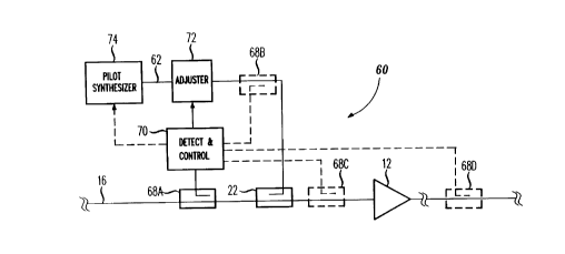
2o FIG. 3 shows a general block diagram of a pilot level adjusting system 60
which
adjusts the power level of a pilot signal on the pilot signal injection path
62 relative to
the power level of an input signal, such as a carrier signal(s), on the main
signal path
16 leading to the RF amplifier 12. A coupler 68a couples a portion of the
input
signal from the signal path 16 before the RF amplifier 12. Detect and control
circuitry 70 determines the power level of the input signal and provides
adjustment
signals to adjuster 72 to adjust the power level of the pilot signal. The
detect and
control circuitry 70 can receive alternative and/or additional inputs shown by
the
dotted lines and couplers 68b-d to provide power level information. Other
inputs are
also possible depending on the application. In certain embodiments, the detect
and
3o control circuitry 70 provides adjustment signals such that the changes in
the power
CA 02275842 1999-06-21
Zhou 3 7
level of the pilot signal track the changes in the power level of the input
signal.
Alternatively, the adjustment signals can be determined based on the input
signal
power level to maintain a desired input signal to pilot signal ratio or
retrieved from a
look-up table based on the input signal power level. Additionally, the
adjustment
signals can be determined to provide an input signal to pilot signal ratio
based on the
degree of correction performed by correction circuitry compared to that
desired.
A pilot synthesizer 74 produces the pilot signal on the pilot injection path
12.
The pilot signal can be a continuous wave (CVO pilot, a spread spectrum pilot,
a
modulated pilot, a pilot of varying frequency, or a pilot having different
frequency
1o components. The coupler 22 then injects the pilot signal into the signal
path 16
before the RF amplifier 12. After being amplified by the amplifier 12, the
feed
forward correction scheme (FIG. 2) as known in the art attempts to cancel the
pilot
signal from the signal path 16, thereby reducing the distortion. If the pilot
signal
level remains the same while the input signal level is reduced at the input to
the RF
15 amplifier 12, the feed forward correction circuitry (FIG. 2) must cancel
more of the
output pilot signal to maintain an acceptable output signal to pilot signal
ratio at the
coupler 38 (FIG. 2) of the feed forward correction circuitry (FIG. 2). If not,
the pilot
signal can result in distortion. By maintaining the power level of the pilot
relative to
the power level of the input signal, the desired input signal to pilot ratio
can be
2o achieved and/or maintained, and the correction circuitry (FIG. 2) need only
cancel the
pilot signal by the same amount (in dB) at the output of the correction
circuitry (FIG.
2) throughout the input signal range. The reduction of the pilot signal still
leads to
the effective reduction of the IMDs because the power level of the worst-case
INIDs
also follow the power level of the input signal. If the input signal level
increases and
25 the pilot signal remains the same, the worst-case INiDs also increase, and
the
correction circuitry (FIG. 2) may fail to cancel the distortion.
FIG. 4 shows an embodiment of a pilot level adjusting system 80 according to
the principles of the present invention. In this embodiment, the coupler 68a
provides
a sample of the input signals) on the signal path 16, and an RF power detector
82
3o provides a voltage signal representing the input power level. The pilot
level adjusting
CA 02275842 1999-06-21
Zhou 3 8
system 80 uses a controller 84 which digitizes the output of the RF power
detector 82
and programs a digital attenuator 86 to provide the appropriate power level
for the
pilot signal depending upon the input power level. For example, to achieve a
30dB
ratio between the input signal power level and the pilot power level, a 2dBm
input
power level would result in a -28 dBm pilot signal power level at the input to
the RF
amplifier 12.
The controller 84 can continuously monitor the input power level. For
example, a sample of the input power level can be taken every microsecond. In
response to the input power level and/or a change in the input power level,
the
controller 86 can determine the appropriate power level and/or attenuation
level for
the pilot signal given the desired input signal to pilot signal ratio. The
controller 84
then provides the corresponding control signals to the digital attenuator 86.
Alternatively, the controller 84 could retrieve the appropriate power level
and/or
attenuation level from a look up tables) and provide the corresponding control
signals to the digital attenuator 86. As such, the pilot level adjusting
system can
maintain an adequate input signal to pilot ratio and enable the feed forward
correction
circuitry (FIG. 2) to more easily cancel the pilot signal while still reducing
the IMDs
to produce an output having a desired output signal to distortion (including
pilot
signal and IMD's) ratio. Depending on the application, different embodiments
can
2o use different sampling rates of the input signal, and the controller 84 can
dynamically
change the power level of the pilot signal with changes to the input signal.
The
changes to the input signal can be based on the latest sample of the power
level of the
input signal, on the average of several power level samples of the input
signal.
Alternative embodiments can measure other characteristics or parameters of the
input
signal. The controller 84 could also provide control signals that result in a
change in
the input signal to pilot signal ratio depending on the power level of the
input signal
or other characteristics or parameters of the input signal. As such, a desired
input
signal to pilot signal ratio or a desired relative difference between
parameters of the
input signal and pilot signal can be provided depending on the input signal
power
level or other parameters of the input signal.
CA 02275842 1999-06-21
Zhou 3 9
FIG. 5 shows an embodiment of a pilot level adjuster 90 where measurements
of the input power level and the adjusted pilot power level are used to adjust
the pilot
power level. The pilot level adjuster locks or synchronizes the adjusted pilot
power
level to the input power level. In this embodiment, the coupler 68a provides a
sample
of the input power level on the signal path 16 to a RF power detector 92, and
the
coupler 68b provides a sample of the adjusted pilot signal on the pilot
injection path
62 to a RF power detector 94. The input power level detector 92 produces a
voltage
signal representative of the input power level, and the pilot power level
detector 94
produces a voltage signal representative of the adjusted pilot level. The
outputs of the
1o two detectors 92 and 94 are provided as the inputs of a control arrangement
96. The
output of the control arrangement 96 controls a voltage controlled attenuator
(VCA)
98 located after the pilot synthesizer 74. Using an infinite gain op-amp
configuration
in this embodiment, the output of the control arrangement 96 adjusts the
attenuation
of the VCA 98 until the two inputs from the RF detectors 92 and 94 are equal.
Other
circuit configurations are possible.
It is possible to maintain a relatively constant input signal to pilot iatio
by
maintaining an offset or power level difference between the input signal and
the pilot
signal at the input to the amplifier 12. To set a desired constant input
signal to pilot
ratio, an offset or difference between the input power level and the pilot
power level
2o is established and maintained. An attenuator(s) 100 can be placed at
different points
to provide the desired difference or offset between the input power level and
the pilot
power level on the main path 16. In determining the appropriate level of
attenuation
for the attenuator(s) 100, the losses introduced by the couplers 68a-b and 22
should
be considered. A typical coupler can introduce l OdB of attenuation on the
secondary
leg of the coupler and .5 dB on the main leg. For example, the coupler 68a
provides
l OdB of attenuation to the input signal coupled onto the input power
detection path
102 from the secondary leg of the coupler 68a and .5 dB of attenuation of the
input
signal on the main path 16 from the main leg of the coupler 68a. Different
types of
couplers and/or coupling devices can be used. For example, a 3 dB splitter
could be
3o used in place of the coupler 68b which splits the pilot signal onto the
pilot injection
CA 02275842 1999-06-21
Zhou 3 10
path 62 and the pilot injection path 104 and attenuates the pilot signal by
3dB on both
paths 62 and 104. In this embodiment, an attenuator 100 is connected between
the
coupler 68b and the input coupler 22 on the pilot signal injection path 62 to
provide a
constant difference between the input power level and the pilot power level at
the
input to the amplifier 12, thereby maintaining the input signal to pilot
ratio.
Alternative configurations are possible to establish the constant difference
or offset
between the input signal power level and the pilot power level.
Alternative embodiments can provide a variable input signal to pilot signal
ratio at the input to the amplifier 12 by varying the offset between the input
signal
1o power level and pilot signal power level at the input to the amplifier 12.
The amount
of offset can dynamically change depending on changing operating performance,
parameters or characteristics, such as input signal level or based on the
degree of
correction and/or distortion measured at the output of the correction
circuitry which
can be compared to a desired operating performance or a previous degree of
performance. The variable input signal to pilot signal ratio can be
dynamically
changed by using a variable attenuator, which can be controlled to achieve the
desired
varying offset, rather than the fixed attenuator(s) 100, and/or by changing
the manner
in which the VCA 98 is controlled.
In this embodiment, as the RF input power level changes, the output of the op-
2o amp arrangement 96 will automatically adjust the VCA 98 until the output of
the pilot
detector 94 equals the output of the input power detector 92. As such, the
pilot power
level is synchronized or locked with the input signal power level. By setting
the
desired offset between the input signal and pilot signal, the desired ratio
between
them can be achieved and maintained. This implementation is simple and in-
expensive. Crude detectors 92 and 94 with non-linear voltage vs. power
characteristic curves could be used, but as long as the two detectors 92 and
94 provide
similar or matching responses over the input range of the RF amplifier 12, the
system
90 should maintain the offset between the input power level and the pilot
power level.
Additionally, the VCA 98 could have a poor voltage vs. attenuation curve, but
the
control arrangement still maintains the desired input signal to pilot signal
ratio. Since
CA 02275842 1999-06-21
Zhou 3 11
the control arrangement 96 attempts to equalize the adjusted pilot level and
the input
power level (minus relative offsets) by adjusting the pilot power level, the
closed loop
configuration of the system 90 maintains the offset between the pilot power
level and
the input power level, thereby maintaining the input signal to pilot signal
ratio.
FIG. 6 shows a detailed embodiment 110 of the pilot level adjuster 90 of FIG.
5. The pilot synthesizer 74 generates the desired pilot signal with a
particular power
level. Using the configuration of FIG. 6, the VCA 98 can be a simple, low-cost
pin-
diode attenuator that has an attenuation range of for example 40dB and a
nonlinear
voltage vs. attenuation curve. In this embodiment, the coupler 68b is a 10 dB
coupler
1o that couples the energy offthe adjusted pilot from the pilot injection path
62. The 10
dB coupler 68b replicates the adjusted pilot onto a pilot detection path 104,
so the
sample of the pilot signal on the pilot detection path 104 is attenuated by
about 10 dB.
The coupler 68b attenuates the adjusted pilot on the pilot injection path 62
by about .5
dB. The sample of the pilot signal on the pilot detection path 104 is provided
to the
pilot detector 94. In this embodiment, the pilot detector 94 is simply a zero-
biased
Schottky diode detector which is not a highly linear RMS RF power detector.
The
pilot detector 94 does have operating characteristics that match the response
of the
input power detector 92 over the input range for the RF amplifier 12.
Accordingly, in
this embodiment, the input power detector 92 is also shown as a simple zero-
biased
2o Schottky diode detector. The pilot power detector 94 provides a pilot power
detection
signal in response to the pilot signal on the pilot power detection path 104.
The input power detector 92 receives a sample of the input signal from the
coupler 68a. The coupler 68a replicates the input signal onto an input signal
detection path 102, so the sample of the input signal on the input signal
detection
path 102 is attenuated by about l OdB. As mentioned above for the coupler 68b,
the
coupler 68a attenuates the input signal on the main signal path 16 by about .5
dB.
The input power detector 92 produces an input power detection signal in
response to
the sample of the input signal on the input signal detection path 102.
In this embodiment, the control arrangement 96 is an operational amplifier
arrangement 96. The op-amp arrangement 96 includes an op-amp 112 and its
CA 02275842 1999-06-21
Zhou 3 12
associated feedback network 114, which maintains the circuit stability and
sets the
response time (for example, 1 millisecond to 1 microsecond or less depending
on the
application). The op-amp arrangement 96 receives the input power detection
signal
from the input power detector 92 and the pilot power detection signal from the
pilot
power detector 94 and attempts to maintain them equal. In this embodiment, two
non-inverting amplifiers 116 and 118 amplify the respective outputs of the
input
power detector 92 and the pilot power detector 94 to improve detection
resolution.
As the input power level changes, the op-amp arrangement 96 maintains the
desired
offset between the input power level and the pilot power level by adjusting
the pilot
1o power level relative to the input power level. To do so, the op-amp
arrangement 96
provides a control signal to the VCA 98 which changes the level of attenuation
for the
pilot signal on the pilot injection path 12 to equalize the inputs to the op-
amp
arrangement 96, thereby reflecting changes in the input power level. In this
embodiment, the control signal is a voltage signal which decreases (increases)
in
voltage when the input power level decreases (increases) to increase
(decrease) the
attenuation of the pilot signal on the pilot injection path 62.
The adjusted pilot signal on the pilot injection path 62 is attenuated by an
attenuator 100 on the pilot inj ection path 62 to set the input signal power
to pilot
signal power ratio. The attenuator 100 can be a fixed valued pi-pad attenuator
(using
3 resistors as would be understood by one skilled in the art). The attenuation
value
for the attenuator 100 along with the relative losses experienced by the input
signal,
the pilot signal and the samples thereof set the desired input signal to pilot
ratio
initially. Once set, the system 110 maintains the ratio between the input
signal power
level and the pilot power level as the input power level changes. The adjusted
pilot
signal from the attenuator 100 is injected onto the main signal path 16 using
the
coupler 22. In this embodiment, the coupler 22 is a 10 dB coupler that couples
the
adjusted pilot with l OdB of attenuation into the signal path 16 to the RF
amplifier 12.
Depending on the particular application, the attenuator 100 in the pilot
injection path
62 can be removed and the relative difference between the input power level
and the
3o pilot power level be established with attenuator(s) on the input power
detection path
CA 02275842 1999-06-21
Zhou 3 13
102 and/or on the pilot power detection path 104. Alternatively, a variable
input
signal to pilot signal ratio can be achieved by using a variable attenuator(s)
100
and/or controlling the VCA to provide the desired variable offset.
For an example implementation in which a difference of 30dB is desired and
s maintained between the input power level and the pilot power level at the
input to the
RF amplifier 12, the input power level is at 2dBm and the pilot synthesizer 74
produces a pilot signal at 5 dBm. For discussion purposes and ignoring the
losses
across the main legs of the couplers 22 and 68a-b, a pilot power level of -
28dBm is
desired at the output of the coupler 22 for a 2dBm input power level. The VCA
98
can be initially set as providing 3dB of attenuation to the SdBm pilot signal
from the
pilot synthesizer 74, thereby providing a 2dBm pilot signal on the pilot
injection path
62. The coupler 68b on the pilot injection path 62 replicates the adjusted
pilot signal
onto the pilot power detection path 104 and attenuates the adjusted pilot on
the pilot
detection path 104 by l OdB so that the pilot power level on the pilot power
detection
~s path 104 is -8dBm. The coupler 68b also provides the adjusted pilot signal
from the
main leg of the coupler 68b onto the pilot injection path 62 to an attenuator
100.
To maintain the 30dB ratio between the input power level (2d.Bm in this
example assuming no attenuation on the main legs of the couplers 68a and 22)
and
the pilot power level at the input to the RF amplifier 12, the pilot power
level should
2o be equal to -28bBm at the input to the RF amplifier. In this example, to
achieve a
pilot signal level of -28 dBm at the RF amplifier 12, the attenuator 100 on
the pilot
injection path 62 is set to provide 20dB of attenuation to the adjusted pilot
signal on
the pilot injection path 62. In this example, the attenuator 100 receives the
adjusted
pilot signal at 2dBm and attenuates the adjusted pilot signal by 20dB to -18
dBm.
25 The adjusted pilot signal at -l8dBm is provided to the secondary leg of the
coupler 22
which attenuates the adjusted pilot signal by l OdB and injects the pilot
signal onto the
main path 16 at -28dBm.
The input signal is received by the coupler 68a, and a sample of the input
signal is produced at the secondary leg of the coupler 68a onto the input
signal
3o detection path 102. In this example, the coupler 68a attenuates the sample
produced
CA 02275842 1999-06-21
Zhou 3 14
on the input power detection path by 10 dB to -8 dBm. As such, the input
signal
power level on the input signal power detection path 102 and the pilot power
level on
the pilot power detection path 104 are equal at -8 dBm. If the input signal
power
level drops, the input signal power level on the input signal detection path
102 drops.
In response, the control arrangement 96 attempts to equalize the input to the
pilot
power detector 94 with the input to the pilot power detector 94 by increasing
the
attenuation of the VCA 98 via a control signal on the control line 120.
For example, if the input signal drops to -1 dBm, the input signal on the
input
power detection path 102 drops to -11 dBm. The op-amp arrangement 96 attempts
to
equalize the -8 dBm pilot signal on the pilot power detection path 104 with
the -11
dBm signal on the input power detection path 102 by increasing the attenuation
of the
VCA 98 on the pilot injection path 62. When the VCA attenuates the pilot
signal by
6dB to -1 dBm at the input to the coupler 68b, the pilot signal on the pilot
power
detection path 104 reaches -11 dBm, and the pilot signal at the input of the
RF
amplifier 12 reaches -3ldBm. Thus, the ratio of the input signal power level (-
1 dBm
in this example) and the pilot power level (-31 dBm) at the input to the RF
amplifier
12 is maintained at 30dB for changing input signal power levels.
In addition to the embodiments described above, alternative configurations of
the pilot level adjustment system according to the principles of the present
invention
2o are possible which omit and/or add components and/or use variations or
portions of
the described system. For example, the example above is provided for
discussion
purposes to show how the pilot level adjuster can provide and maintain a 30dB
offset
between the input power level and the pilot power level on the signal path 16.
Depending on the particular design and the input voltage v. attenuation
characteristics
of the variable attenuator on the pilot injection path, the pilot adjusting
system can
maintain the desired offset between the pilot power level and the input power
level
for different ranges of input signal power levels. To take advantage of the
full range
of attenuation provided by the variable attenuator, the various signal power
levels
must be considered and additional attenuators or components which can
attenuate
signals can be placed in the various paths. Additionally, variable attenuators
or
CA 02275842 1999-06-21
Zhou 3 1 S
attenuation arrangements with increased attenuation ranges can be used to
increase
the range of input signal power levels in which the pilot adjusting system
provides the
desired ratio between the input signal power level and the pilot power level.
The pilot adjusting system has been described as using couplers, but 3dB
splitters and other coupling, signal splitting or sampling devices can be used
in place
of the couplers. Additionally, the pilot adjusting system is described with
fixed
attenuators, but variable attenuators or other devices which provide signal
attenuation
can be used in place of the fixed attenuators. Such a variable attenuator can
be
controlled to dynamically change the input power level to pilot power level
ratio.
1o The pilot level adjustment system has been further described as using
different
configurations of discrete components, but it should be understood that the
pilot level
adjustment system and portions thereof can be implemented in application
specific
integrated circuits, software-driven processing circuitry, firmware or other
arrangements of discrete components as would be understood by one of ordinary
skill
in the art with the benefit of this disclosure.
The embodiments of the pilot adjustment system have been described as being
used with feed-forward RF amplifier arrangements, but the pilot adjustment
system
can be used in any amplifier arrangement where a pilot signal is used and the
input
pilot power level is adjusted relative to the input power. Additionally, the
pilot
2o adjusting system has been described as adjusting the pilot power level
relative to an
input signal power level, but the pilot adjusting system can adjust pilot
power level
based on the averages of multiple Garners or signals, the highest power level
carrier
or signals and/or combinations thereof related to input power level.
Furthermore, the
pilot adjustment system has been described as adjusting pilot signal power
level
relative to input signal power level, but other parameters or characteristics
of the pilot
signal can be adjusted based on the characteristics or parameters of the input
signal.
What has been described is merely illustrative of the application of the
principles of
the present invention. Those skilled in the art will readily recognize that
these and
various other modifications, arrangements and methods can be made to the
present
3o invention without strictly following the exemplary applications illustrated
and
CA 02275842 1999-06-21
Zhou 3 16
described herein and without departing from the spirit and scope of the
present
invention.