Note: Descriptions are shown in the official language in which they were submitted.
CA 02276251 1999-06-30
WO 98/22625 PCT/US97/21333
DESCRIPTION
MICROFABRICATED ISOTHERMAL NUCLEIC ACID AMPLIFICATION DEVICES AND METHODS
BACKGROUND OF THE INVENTION
1. Field of the Invention
The present invention relates generally to the field of molecular biology, and
relates to
methods for amplifying nucleic acid target sequences in mierofabricated
devices. It particularly
relates to isothermal methods for amplifying nucleic acid targets in
microfabricated devices. The
present invention also relates to methods of detecting and analyzing nucleic
acids in
microfabricated devices.
2. Description of Related Art
In vitro nucleic acid amplification techniques have provided powerful tools
for detection
and analysis of small amounts of nucleic acids. The extreme sensitivity of
such methods has lead
to their development in the fields of diagnosis of infectious and genetic
diseases, isolation of
genes for analysis, and detection of specific nucleic acids as in forensic
medicine.
I S Nucleic acid amplification techniques may be grouped according to the
temperature
requirements of the procedure. Certain nucleic acid amplification methods,
such as the
polymerase chain reaction (PCRTM - Saiki et al., 1985), ligase chain reaction
(LCR - Wu et al.,
1989; Barnnger et al., 1990; Barony, 1991 ), transcription-based amplification
(Kwoh et al.,
1989) and restriction amplification (U.S. Patent No. 5,102,784), require
temperature cycling of
the reaction between high denaturing temperatures and somewhat lower
polymerization
temperatures. In contrast, methods such as self sustained sequence replication
(3SR; Guatelli et
al., 1990), the Qp replicase system (Lizardi et al., 1988), and Strand
Displacement Amplification
(SDA - Walker et al., 1992a, 1992b; U.S. Patent No. 5,455,166) are isothermal
reactions that are
conducted at a constant temperature, which is typically much lower than the
reaction
temperatures of temperature cycling amplification methods.
The SDA reaction initially developed was conducted at a constant temperature
between
about 37°C and 42°C (U.S. Patent No. 5,455,166). This was
because the exo-klenow DNA
polymerase and the restriction endonuclease (e. g. , HindII) are mesophilic
enzymes that are
CA 02276251 1999-06-30
WO 98/22625 PCT/LTS97/21333
2 -
thermolabile (temperature sensitive) at temperatures above this range. The
enzymes that drive
the amplification are therefore inactivated as the reaction temperature is
increased.
_ Methods for isothermal Strand Displacement Amplification, which may be
performed in
a higher temperature range than conventional SDA (about 50°C to
70°C, "thermophilic SDA"),
were later developed. Thermophilic SDA is described in European Patent
Application No.
0 684 315 and employs thermophilic restriction endonucleases that nick the
hemimodified
restriction endonuclease recognition/cleavage site at high temperature and
thermophilic
polymerases that extend from the nick and displace the downstream strand in
the same
temperature range.
Photolithographic micromachining of silicon has been used to construct high-
throughput
integrated fluidic systems for a variety of chemical analyses. This technology
is of particular
interest for the development of devices for analysis of nucleic acids, as in
their conventional
formats such analyses are typically labor- and material-intensive. Ideally,
all of the processing
steps of the amplification reaction would be conducted on the microfabricated
device to produce
1 S a completely integrated nucleic acid analysis system for liquid transfer,
mixing, reaction and
detection that requires minimal operator intervention.
Silicon and glass devices are economically attractive because the associated
micromachining methods are, essentially, photographic reproduction techniques.
Silicon
structures are processed using batch fabrication and lithographic techniques.
These processes
resemble those of printing where many features may be printed at the same
time. These
processes permit the simultaneous fabrication of thousands of parts in
parallel, thus reducing
system costs enormously. Today, silicon fabrication techniques are available
to simultaneously
fabricate micrometer and submicrometer structures on large-area wafers { 100
cm2), yielding
millions of devices per wafer and may be used to process either silicon or
glass substrates.
These characteristics have led to the proposal of silicon and glass as a
candidate
technology for the construction of high-throughput DNA analysis devices
(Woolley and Mathies,
1994; Northrop et al., 1993; Effenhauser et al., 1994). As mechanical
materials, both silicon and
glass have well-known fabrication characteristics (Petersen, 1982).
Microfabricated devices for
biochemical and fluidic manipulation are undergoing development in many
laboratories around
the world (Ramsey et al., 1995; McIntyre 1996). Over the past 10 years, a
number of
CA 02276251 1999-06-30
WO 98/22625 PCT/US97/21333
3
microfluidic devices have been developed that allow the construction of
miniaturized "chemical
reactors." Individual components of the system such as pumps (Esashi et al. ,
1989; Zengerle et
al., 1992; Matsumoto and Colgate, 1990; Folta et al., 1992); valves (Esashi et
al., 1989, Ohnstein
et al., 1990; Smits, 1990); fluid channels (Pfahler et al., 1990);
chromatographic and liquid
electrophoresis separation systems (Terry et al., 1979; Harnson et al., 1992b-
g; Manz et al.,
1991; Manz et al. , 1992) are available. Although an obj ective of several
research groups,
complete silicon-fabricated nucleic acids analysis systems are still at the
earliest stages of
development.
Other components that have been microfabricated which are applicable to
nucleic acid
analysis include elements for gel electrophoresis (Zeineh and Zeineh, 1990;
Helier and Tullis,
1992; Effenhauser et al., 1994; Woolley and Mathies, 1994, 1995; Webster et
al., 1996);
capillary electrophoresis (Mann et al. 1992, 1995; Effenhauser et al., 1993;
Fan and Harnson,
1994; Jacobsen et al., 1994a; 1994b; Jacobson and Ramsey, -1995; Ocvirk et
al.) 1995; von
Heeren et al., 1996); synthetic oligonucleotide arrays (Fodor et al., 1993;
Schena et al., 1995;
Hacia et al., 1996); continuous flow pumps {Lintel, 1988; Esashi et al., 1989;
Matsumoto and
Colgate, 1990; Nakagawa et al.) 1990; Pfahler et al., 1990; Smits, 1990;
Willing et al., 1994;
Olsson et al., 1995); discrete drop pumps (Burns et al., 1996); enzymatic
reaction chambers
(Northrop et al., 1994; Willing et al., 1994b; Cheng et al., 1996);
optical/radiation detectors
(Belau et al., 1983; Wouters and van Sprakelaar, 1993; Webster et al., 1996);
and
multicomponent systems (Harrison et al.) 1992, 1995; Northrop et al. 1994;
3acobsob and
Ramsey 1996).
To date, a number of devices have been micromachined, including pumps and
valves
(Gravensen et al. , 1993 ; Manz et al. , 1994; Colgate and Matsumoto, 1990,
Sammorco et al,
1996); reaction chambers (Woolley and Mathies, 1994; Willing et al., 1994);
and separation and
detection systems (Weber and May, 1989, Northrop et al., 1993, Harrison et
al., 1993; Manz et
al., 1992; Jacobson et al., 1994; Schoonevald et al., 1991; Van den Berg and
Bergveld, 1995;
Woolley et al., 1995). Some of these have been recently integrated together to
build
pharmaceutical drug closing systems (Lammerink et al., 1993; Miyake et al.,
1993) and other
microchemical systems (Nakagawa et al., 1990; Washizu, 1992; Van den Berg and
Bergveld,
1995). One device is an integrated glass system combining DNA restriction
enzyme digestion
and capillary electrophoresis (Jacobson and Ramsey 1996). An alternative
format using high-
CA 02276251 1999-06-30
WO 98/22625 PCT/US97/21333
4
density arrays of synthesized oligodeoxynucleotides has been demonstrated as a
DNA sequence
detector (Fodor et al., 1993; Hacia et al., 1996).
Nucleic acid targets have been successfully amplified by the PCRTM on such
microfabricated devices, often referred to as "chips" (U.S. Patent No.
5,498,392; Woolley et al.,
1996; Shoffner et al., 1995; Cheng et al., 1996; Wilding et al., 1994; U.S.
Patent No. 5,589,136;
U.S. Patent No. 5, 639,423; U.S. Patent No. 5,587,128, U.S. Patent No.
5,451,500) and LCR
(Cheng et al., 1996; U.S. Patent No. 5,589,136). Evaporation due to repeated
exposure to high
temperatures during thermocycling is a problem. Evaporation during PCRTM has
been controlled
by immersing the channel in oil such that the open ends are covered, but this
makes recovery of
the amplified sample difficult.
SUMMARY OF THE INVENTION
The present invention overcomes the foregoing evaporation and recovery
drawbacks, and
other def ciencies inherent in the prior art, by providing compositions and
methods for use in the
isothermal amplification of nucleic acids in microfabricated devices. In
contrast to the
difficulties previously perceived to exist and the prejudices in the art, the
inventors found
isothermal amplification of nucleic acids using microfabricated devices or
"chips" to be
surprisingly effective. In fact, the chip-based isothermal amplification of
the present invention
was discovered to be efficient at previously untested low temperatures,
despite potentially
negative effects of surface chemistry and other proposed problems, such as
stagnant temperature
gradients, reduced diffusion and mixing, and inhibition of enzyme activity.
The invention thus generally provides an apparatus, system, device or chip, or
a plurality
thereof, with isothermally regulated reaction chambers, methods of
constructing single-chip and
multiple-chip analytical systems, and methods for using such devices, chips
and systems in the
isothermal amplification of nucleic acids. The invention also provides for the
analysis of the
amplification products using, e.g., sequencing, gel separation, and/or
detection of the
amplification products in microfabricated devices. Further methods of the
invention therefore
include laboratory methods connected with nucleic acid analysis and clinical
methods connected
with the diagnosis and prognosis of disease states.
CA 02276251 1999-06-30
WO 98/22625 PCT/US97/21333
First provided by the invention are devices, chips, wafers or an analytical
apparatus or
system(s), generally of a microfabricated or micromachined type, for use in
the isothermal
amplification of selected nucleic acids. Certain preferred devices utilize the
silicon chip or
silicon wafer formats. In preferred embodiments, the devices of the present
invention are
S "microdevices", preferably defining micromachined structures for use with
nanoliter volumes.
The apparati, devices or chips of the invention generally comprise a
microfabricated
substrate or housing defining at least a first transport channel, or
microdroplet transport channel,
operably connected to at least a first reaction chamber, and at least a first
means for isothermally
regulating the temperature of the reaction chamber.
The "means for isothermally regulating the temperature of the reaction
chamber" may be
an element, such as a particular resistor, combination of resistors, feed-back
temperature
detector, and/or circuitry for temperature control, that has not been
previously used in
conjunction with a microfabricated device or chip for use in nucleic acid
amplification. More
preferably, the "means" for isothermally regulating the temperature of the
reaction chamber will
be a "programmable means". That is, a series of executable and controlled
steps, preferably in
the form of a computer program, the implementation of which results in the
control of the
temperature of the reaction chamber within narrow limits, such that the
temperature is
"substantially constant". These computer microprocessor or programmable means,
although
readily prepared by those of skill in the art, have not previously been
proposed for use in
combination with a microfabricated nucleic acid amplification device.
The microfabricated substrate of the device, chip or system is generally
constructed so
that application of a fluid in one or more transport channels will result in
the fluid being
conveyed at least to the reaction chamber. Accordingly, the microfabricated
substrate inherently
has a "flow-directed fabrication". The flow-directed fabrication or
construction may be based
upon gravitational attraction, thermal gradients, gas or liquid pressure
differences, differences in
hydrophobic and hydrophilic surface structures, electrowetting, and/or
differences in the
dielectric constant between reagent fluids applied to the substrate and the
air or surrounding
media. The manner in which a directional flow capability is provided to the
substrate is not
critical to the invention, so long as the substrate, device or system
ultimately allows for the
CA 02276251 1999-06-30
WO 98/22625 PCT/US97/21333
6
controlled manipulation of liquids or fluids applied thereto, and effective
merging and mixing
where appropriate.
In the context of this invention, a "reaction" or "amplification" generally
refers to
reactions involving nucleic acid biomolecules, such as RNA and DNA. "Nucleic
acid
amplification" generally refers to the process of increasing the concentration
of nucleic acid, and
in particular, the concentration of a selected nucleic acid and/or a defined
piece of a selected
nucleic acid. "Amplified or amplification products" or "amplicons" generally
define the products
resulting from execution of a nucleic acid amplification reaction.
As used herein, the term "an isothermal amplification reaction" refers to a
nucleic acid
amplification reaction that is conducted at a substantially constant
temperature. It will be
understood that this definition by no means excludes certain, preferably
small, variations in
temperature but is rather used to differentiate the isothermal amplification
techniques from other
amplification techniques known in the art that basically rely on "cycling
temperatures" in order
to generate the amplified products. Thus, the present invention is
distinguished from PCR,
which fundamentally rests on the temperature cycling phenomenon.
It will be further understood that although the isothermal amplification
reactions of the
present invention will generally be conducted at a substantially constant
temperature, the overall
execution of the amplification, diagnostic or prognostic methods of the
invention may
nonetheless require certain steps to be conducted at different temperatures.
For example, moving
fluids or microdroplets through the different channels or chambers defined on
the
microfabricated substrate, and/or merging and mixing samples and reagents, may
involve
alterations in temperature, e.g., as may be achieved via the use of defined
heating elements.
The microfabricated substrate or housing of the invention may be fabricated
from any one
of a number of suitable materials. The materials will preferably be of the
type that can be
manipulated to define the channels, reaction chambers and other components
necessary for
conducting the amplification methods, and yet will be stable enough to permit
repeated use in
such methods once the defining components have been etched or otherwise
imparted onto the
substrate. Certain preferred examples include, buare not limited to, silicon,
quartz and glass.
CA 02276251 1999-06-30
WO 98/22625 PCT/I1S97/21333
7
The transport channels or "microdroplet transport channels" defined in the
substrate are
generally pathways, whether straight, curved, single, multiple, in a network,
etc., through which
liquids, fluids and/or gases may be passively or actively transported. The
channels are generally
etched into the silicon, quartz, glass or other supporting substrate. The
present invention requires
the presence of at least a first channel that functions to allow the transport
of a fluid sample into
the reaction chamber. It will be understood that such a channel need not be of
a significant
minimum length, and that the term "channel" therefore refers to a fluid-
conveying section in
functional terms, rather than to defining a structure that is necessarily long
and pipe-like.
The one or more channels in the substrate connect the various components,
i.e., keep
components "in communication" and more particularly, "in fluidic
communication" and still
more particularly, "in liquid communication." Such components include, but are
not limited to,
gas-intake channels and gas vents. In certain other aspects of the invention
"microdroplet
transport channels" may refer to channels configured (in microns) so as to
accommodate
"microdroplets."
While it is not intended that the present invention be limited by precise
dimensions of the
channels or precise volumes for microdroplets, illustrative ranges for
channels may be between
0.5 and 50/pm in depth (preferably between 5 and 20 pm) and between 20 and
1000/~m in width
(preferably S00/pm), and the volume of the microdroplets may range (calculated
from their
lengths) between approximately 0.01 and 100 nanoliters (more typically between
ten and fifty).
The first microdroplet transport channel may be operably or functionally
connected to, or
in liquid communication with, at least a second microdroplet transport
channel. First and second
channels may operatively interact prior to connection with at least a first
isothermally regulated
reaction chamber. This would be the first meaning of "connective channels".
However, other
operative connections ire envisioned, and separate transport channels that
function to deliver
fluids to a common reaction chamber are still "interactive transport channels"
in the context of
the present invention in that they convey their contents to a common
destination.
The present invention is not limited to the number of transport channels or
other fluid-
conveying means that may be provided in the substrate. The number and
configuration of such
channels will generally be dictated by the number of reaction chambers and
other components
CA 02276251 1999-06-30
WO 98/22625 PCT/US97/21333
8
provided on the substrate and/or the interaction of various individual chip
elements to form a
coordinated system.
At least one isothermally regulated reaction chamber is an important element
of the
present invention. As used herein, an "isothermally regulated reaction
chamber" is a chamber,
preferably one defining a microvolume receptacle, the temperature of which
chamber may be
regulated in order to keep it substantially constant. The "substantially
constant" temperature may
be controlled within a few degrees, or within a single degree, or in certain
embodiments, within a
few tenths of a degree.
The means for isothermally regulating the reaction chamber may include, but
are not
limited to, resistors in contact with or in proximity to the reaction chamber,
temperature
detectors, resistive temperature detectors, dielectric sensors, or diodes
and/or circuitry for
temperature control. As discussed, the isothermal regulation means will
preferably be a
programmable means. The actual means of conveying the heat will preferably be
a sheet
resistively heated (rather than a wire), although polysilicon and doped
polysilicon and
diaphragm-type heaters may also be used in the reaction chamber.
In certain embodiments of the present invention, the microfabricated substrate
further
defines at least a first entry port operably or functionally connected to, or
in liquid
communication with, at least a first microdroplet transport channel. Any one
of a variety of
entry valves or ports may be used to control application of the sample or
samples.
In embodiments where the microfabricated substrate further defines at least a
second
microdroplet transport channel, at Ieast a second entry port may be provided
in operable or
functional connection, or in liquid communication with the second microdroplet
transport
channel. The invention is not limited to the number of transport channels, nor
to the number of
entry ports, either in terms of ports per channel or the total number of entry
ports.
"Exit ports" or "sample collection points" are also envisioned, which are
generally
positioned at a downstream flow site from the reaction chamber.
In certain aspects of the invention, the microfabricated substrate will
further comprise a
flow-directing means system in order to facilitate that directed manipulation
of fluids around the
substrate. The term "flow-directing means system" is intended to refer to one
or more
CA 02276251 1999-06-30
WO 98/22625 PCT/US97/21333
9
modifications of the substrate or other components used in functional
association with the
substrate that act to control, or further control, the transport, merging
and/or mixing of fluids or
microdroplets between the components etched onto the underlying substrate.
Certain preferred flow-directing means systems are those that employ a surface-
tension-
gradient mechanism in which discrete droplets are differentially heated and
propelled through
etched channels. A series of heating elements may thus be arrayed along the
one or more
microdroplet transport channels. Such resistive heaters may be located
slightly beneath the
channels. In certain aspects of the invention, the heating elements are
comprised of aluminum,
although one or more or a combination of other suitable resistive metals or
materials may be
employed, such as platinum, gold, etc.
In certain aspects of the invention, "heating element" may refer to an element
that is
capable of at least partially liquefying a meltable material. A meltable
material is "associated
with" a heating element when it is in proximity to the heating element such
that the heating
element can at least partially melt the meltable material. The proximity
necessary will depend on
the melting characteristics of the meltable material as well as the heating
capacity of the heating
element. The heating element may or may not be encompassed within the same
substrate as the
meltable material.
Other fluid-directing means systems for use in the invention are those that
comprise a gas
source in fluid communication with the one or more transport channels and
other components,
such that application of differential gas pressure gradients result in the
controlled flow of gases
or liquids through the micromachined device.
Differences in hydrophobic and hydrophilic surface structures may also be
employed to
control the flow or transport of fluids through the defined channels and
etched components. In
such embodiments, the transport channels and/or components may comprise or may
be
manipulated to comprise one or more hydrophobic regions. The channels and
components may
also be treated with a hydrophilicity-enhancing compound or compounds prior to
addition of one
or more of the biological samples or amplification reaction reagents.
"Hydrophilicity-enhancing compounds" are generally those compounds or
preparations
that enhance the hydrophilicity (water affinity) of a component, such as a
transport channel.
CA 02276251 1999-06-30
WO 98/22625 PCT/US97/21333
"Hydrophilicity-enhancing compound" is thus a functional term, rather than a
structural
definition. For example, Rain-XTM anti-fog is a commercially available reagent
containing
glycols and siloxanes in ethyl alcohol. The fact that Rain-XTM anti-fog
renders a glass or silicon
surface more hydrophilic is more important than the reagent's particular
formula.
5 In certain aspects of the invention "hydrophobic reagents" are used to make
"hydrophobic
coatings" and create "hydrophobic regions" (more water repellent) in channels.
It will be
understood that the present invention is not limited to particular hydrophobic
reagents. In one
embodiment, the present invention contemplates hydrophobic polymer molecules
that may be
grafted chemically to the silicon oxide surface. Such polymer molecules
include, but are not
10 limited to, polydimethylsiloxane. In another embodiment, the present
invention contemplates the
use of silanes to make hydrophobic coatings, including but not limited to
halogenated silanes and
alkylsilanes. The invention is not limited to particular silanes; the
selection of the silane is only
limited in a functional sense, i. e., that it render the surface hydrophobic.
In one embodiment, n-octadecyltrichlorosilane (OTS) is used as a hydrophobic
reagent.
In another embodiment, octadecyldimethylchlorosilane is employed. In yet
another embodiment,
the invention contemplates 1 H, 1 H, 2H, 2H-perfluorodecyltricholorosilane
(FDTS,
C ~ oH4F, ~SiCl3) as a hydrophobic reagent. In still other embodiments,
fluoroalkyl-, aminoalkyl-,
phenyl-, vinyl-, bis silyl ethane- and 3-methacryloxypropyltrimethoxysilane
(MAOP) are
contemplated as hydrophobic reagents. Such reagents (or mixtures thereof) are
useful for
making hydrophobic coatings, and more preferably, useful for making regions of
a channel
hydrophobic (as distinct from coating the entire channel).
This invention is not limited to particular dimensions for the hydrophobic
regions of the
channels or components. However, while a variety of dimensions are possible,
it is generally
preferred that the regions have a width of between approximately 10 and 1000
p,m (or greater if
desired), and more preferably between approximately 100 and 500 p,m.
A surface (such as a channel surface) is "hydrophobic" when it displays
advancing
contact angles for water greater than approximately 70°. In one
embodiment, the treated channel
surfaces of the present invention display advancing contact angles for water
between
approximately 90° and approximately 130°. In another embodiment,
the treated microchannels
have regions displaying advancing contact angles for water greater than
approximately 130°.
CA 02276251 1999-06-30
WO 98/22625 PCT/L1S97/21333
11
In certain aspects of the invention, a "liquid-abutting hydrophobic region"
may refer to a
hydrophobic region within a channel which has caused liquid (e.g., aqueous
liquid) to stop or be
blocked from further movement down the channel, said stopping ar blocking
being due to the
hydrophobicity of the region, said stopped or blocked liquid positioned
immediately adjacent to
said hydrophobic region.
Other flow-controlling or flow-directing means systems contemplated for use in
the
present invention are those that rely on the phenomenon of electrowetting,
and/or differences in
the dielectric constant between the reagent fluids and air. Electrowetting may
be described as the
initial intake of fluid from a reservoir into a channel, electrowetting (or
heating) may also be
used to break the channel droplet from contact with the reservoir. Valve
sealed by a movable
diaphragm and/or meltable solder can also be used to control fluid flow.
Any one of a variety of pumps, both external and internal pumps, may be used
in order to
control the flow of fluids in the context of this invention. In certain
aspects of the invention a
"bubble pump" may be used as a flow-directing means. A bubble pump operates as
follows:
fluid is introduced into a channel that comprises one or more electrodes
positioned such that they
will be in contact with a liquid sample placed in the channel. Two electrodes
may be employed
and a potential may be applied between the two electrodes. At both ends of the
electrodes,
hydrolysis takes place and a bubble is generated. The gas bubble continues to
grow as the
electrodes continue pumping electrical charges to the fluid. The expanded
bubble creates a
pressure differential between the two sides of the liquid drop which
eventually is large enough to
push the liquid forward and move it through the polymer channel.
When coupled with a capillary valve, a bubble pump can actuate an effective
quantity of
fluidic samples along the channel. The capillary valve is a narrow section of
a channel. In
operation, the fluidic sample is first injected into an inlet reservoir. As
soon as the fluid is
loaded, it moves in the channel by capillary force. The fluid then passes the
narrow section of
the channel but stops at the edge where the channel widens again. After the
fluidic sample is
loaded, a potential is applied between two electrodes. At both ends of the
electrodes, hydrolysis
occurs and bubble is generated. The bubble keeps growing as the electrodes
continue pumping
electrical charges to the fluid. The expanding bubble then creates a pressure
differential between
the two sides of the liquid drop, which eventually large enough to push the
liquid forward.
CA 02276251 1999-06-30
WO 98/22625 PCT/US97121333
12
The combination of bubble pump and capillary valve does not require any moving
parts
and is easy to fabricate. In addition, the device produces a well-controlled
fluid motion, which
depends on the bubble pressure. The bubble pressure is controlled by the
amount of charges
pumped by the electrodes. The power consumption of the device is also
minimized by this
method.
In certain aspects of the invention, the flow-directing means is separated
from at least the
first microdroplet transport channel by a liquid barner. "Liquid barner" or
"moisture barner"
refers to any structure or treatment process on existing structures that
prevents short circuits
and/or damage to electronic elements (e.g., prevents the destruction of the
aluminum heating
elements). In one embodiment, the liquid barrier may comprise a first silicon
oxide layer, a
silicon nitride layer and a second silicon oxide layer.
Further preferred aspects of the invention are those wherein the
microfabricated substrate
further defines, or is operably associated with, a nucleic acid analysis
component operably
connected to or in liquid communication with the isothermally regulated
reaction chamber. The
operative connection between the nucleic acid analysis component and the
reaction chamber is
such that the amplified nucleic acid products generated by the isothermal
amplification reaction
can be analyzed by the nucleic acid analysis component. The overall analytical
method thus
requires that the amplified products are conveyed or otherwise transported
from the isothermally
regulated reaction chamber to the nucleic acid analysis component in a manner
effective to allow
their subsequent analysis, separation, detection, or such like.
Any one of a variety of nucleic acid separation and analytical components may
be used as
part of the devices or systems of the present invention. Amplification product
separation means
include those for use in separation methods based upon chromatographic
separation, including
adsorption, partition, ion-exchange and molecular sieve, and techniques using
column, paper,
thin-layer and gas chromatography. Gel electrophoresis, liquid capillary
electrophoresis, e.g., in
glass, fused silica, coated and rectangular column format, polyacrylamide gel-
filled capillary
columns are particularly contemplated. Gel electrophoresis channels and/or
capillary gel
electrophoresis channels may thus be etched into the substrate.
The use of a miniature electrophoresis stage for macromolecule DNA separation
is also
contemplated. Using such a system can accomplish large savings of time and
funds by a
CA 02276251 1999-06-30
WO 98/22625 PCT/US97/21333
13
reduction in sample size, an increase in processing system speed of the
system, a increase in the
number of samples handled through massive parallelism and batch fabrication
techniques.
In certain embodiments, the present invention will comprises a nucleic acid
detection
means operably connected to, or in electrical communication with, the nucleic
acid analysis
component. Visualization means particularly envisioned include those using
ethidium
bromide/UV and radio or fluorometrically-labeled nucleotides, including
antibody and biotin
bound probes. The nucleic acid detection means may thus include, but is not
limited to, a diode
detection device with suitable filters for detection of radioactive decay,
fluorescence, visible and
nonvisible light wavelengths, and/or electromagnetic field changes.
The nucleic acid detection means may be a DNA sensor means, e.g., one that
detects a
radiolabel or a fluorescent label. Such DNA sensor means may be p-n-type
diffusion diodes or
p-n-type diffusion diodes combined with a wavelength filter and an excitation
source. Silicon
radiation/fluorescence detectors, photodiodes, silicon diffused diode
detectors, and other silicon
fabricated radiation detectors are also contemplated.
1 S The control circuitry for preferable use in the device may be "on wafer
control circuitry"
or "off wafer control circuitry", the latter preferably for use in non-glass
devices. In addition to
the isothermal temperature controls, the control circuitry employed may
include sample size and
flow control circuits; timing circuits; electrophoretic separation bias, data
detection and
transmission control circuits; and one or more sequencer/timers to control the
overall operation.
Thus the instant devices are contemplated for use in conducting a diagnostic
test on a
nucleic acid sample. Additionally, the present devices are contemplated for
use in conducting a
diagnostic or prognostic test on a biological sample suspected of containing a
selected nucleic
acid. Therefore, the present invention provides for the use of the instant
devices in the
manufacture of a kit or system for the amplification of nucleic acids. In
certain aspects, the
invention provides for the use of the present devices in the manufacture of a
kit or system for the
diagnosis or prognosis of a disease.
Any one or more of the isothermal amplification devices or chips of the
present invention
may be formulated or packaged with biological reagents effective to permit an
isothermal nucleic
acid amplification reaction. In such aspects, the combined reagents and
devices may be
CA 02276251 1999-06-30
WO 98/22625 PCT/US97121333
14 -
considered as "isothermal nucleic acid amplification kits". "Biological
reagents effective to
permit an isothermal nucleic acid amplification reaction" are exemplified by
polymerases,
nucleotides, buffers, solvents, nucleases, endonucleases, primers, target
nucleic acids including
DNA and/or RNA, salts, and other suitable chemical or biological components.
The kits may thus be defined as comprising, in suitable container means at
least a first
microfabricated substrate defining at least a first-channel, the at least a
first channel connected to
an isothermally regulated reaction chamber, and reagents effective to permit
an isothermal
amplification reaction.
In such kits, the first microfabricated substrate may further define a nucleic
acid analysis
component operably connected to said isothermally regulated reaction chamber
and, optionally, a
nucleic acid detection means operably connected to the nucleic acid analysis
component.
The biological reagents effective for use in the amplification reactions may
be provided
or packaged in any suitable form, preferably aliquoted into suitable
quantities. In certain
preferred aspects, such reagents will be provided in a dry or lyophilized
formulation. The
provision of reagents, preferably in a lyophilized form, applies to both kits,
in which the reagents
are generally separately packaged, and integral devices, in which the
lyophilized reagents may be
pre-fabricated into one or more etched components on the substrate.
In certain other embodiments, an effective amount of the amplifying reagents
may be
provided in a separate cartridge that is interchangeably connected to the
device, chip or system.
Such replaceable cartridges or reservoirs may be provided in the same overall
container means as
the device, chip or system or may be purchased separately as distinct items.
Different
replaceable cartridges may be provided for conducting the various different
isothermal
amplification reactions that are known in the art. A number of reagent
formulations may be
packaged together for alternative use according to the needs of the end user.
Diagnostic systems are also provided by the present invention, comprising at
least a first
microfabricated substrate defining at least a first channel that is connected
to at least a first
isothermally regulated reaction chamber; wherein the diagnostic system further
comprises a
nucleic acid analysis component and a nucleic acid detection means in operable
association with
the reaction chamber of the microfabricated substrate.
CA 02276251 1999-06-30
WO 98/22625 PCT/US97/21333
The diagnostic systems may also comprise, in operable association, at least a
second
microfabricated substrate defining at least a second channel that is connected
to at least a second
isothermally regulated reaction chamber. Third, fourth, fifth, tenth, 20th,
50th, 100th, 500th and
1000th microfabricated substrates may also be provided, as is the meaning of
"a plurality of
5 microfabricated substrates".
The diagnostic systems may variously have at least a first and at least a
second
microfabricated substrate, or a plurality thereof, that are operably connected
in series to a single
nucleic acid analysis component and nucleic acid detection means. The
diagnostic systems may
alternatively comprise at least a first and at least a second microfabricated
substrate, or a plurality
10 thereof, that are operably connected in parallel to at least two distinct
nucleic acid analysis
components and nucleic acid detection means, or a plurality of such
components.
In such kit and system embodiments, liquid handling, electrophoresis, and
detector
components may be coupled into an integrated format. DNA samples may move
directly
between sample processing, size-separation, and product detection. The
components are
15 controlled by electronic circuitry, fabricated on the same silicon wafer.
Accordingly, an integrated DNA sample processing design may be arrayed as
multiple
parallel units on a single silicon wafer. The number of parallel DNA
processing units per wafer
may be maximized, and circuitry used for overall control. A large number of
simultaneous
isothermal amplification reactions (up to 1000 per wafer) may be performed on
such systems.
Methods of making devices for use in isothermal nucleic acid amplification are
provided
by the invention, which generally comprise preparing at least a first
microfabricated device, chip
or wafer defining at least a first channel that is operably connected to an
isothermally regulated
reaction chamber, preferably isothermally regulated by a programmable means.
A method of making a nucleic acid diagnostic kit is also provided, which
generally
comprises preparing at least a first microfabricated device, chip or wafer
defining at least a first
channel that is operably connected to an isothermally regulated reaction
chamber, and combining
the microfabricated device with biological reagents effective for use in an
isothermal
amplification reaction. The combination may be with lyophilized reagents,
which may further be
disposed in the device as an integral component.
CA 02276251 1999-06-30
WO 98/22625 PCT/I1S97/21333
16
Methods of making a nucleic acid diagnostic system are further provided,
comprising
preparing at least a first microfabricated substrate defining, in a series of
operable associations, at
least a first channel, an isothermally regulated reaction chamber, a nucleic
acid analysis
component and a nucleic acid analysis detection means.
Multi-component nucleic acid diagnostic systems may also be manufactured by
the
methods of the present invention. To make a multi-component nucleic acid
diagnostic system, a
plurality of microfabricated substrates, nucleic acid analysis and detection
means are operably
combined, preferably in an interactive array or arrays. Controlling electronic
circuitry and
programmable regulating means are preferably provided. Multiple parallel unit
arrays on single
silicon wafers are particularly preferred.
Important aspects of the present invention are methods for the isothermal
amplification of
selected nucleic acids or portions thereof, which methods generally comprise
providing or
introducing a microdroplet sample comprising or suspected of comprising the
selected nucleic
acid, and reagents effective to permit an isothermal amplification reaction,
to at least a f rst
microfabricated substrate with an isothermally regulated reaction chamber, as
generally defined
hereinabove, and conducting an isothermally regulated amplification reaction
to amplify the
selected nucleic acid or a portion thereof.
As used herein, the terms "providing" or "introducing" mean that the sample or
samples
are provided or introduced into the one or more microfabricated substrates in
a manner effective
to begin their conveyance, transportation or general movement to the
isothermally regulated
reaction chamber. As described hereinabove, a number of particular flow-
directing means
systems may be employed in order to convey the sample or samples to the
reaction chamber.
Where differential heating is employed as the sole transport means, or as part
of the overall
transport means, an important aspect of the invention is that any samples that
comprise enzymes
for use in the isothermally regulated nucleic acid amplification reaction are
"thermotransported"
at a temperature below the critical temperature of the polymerase enzyme.
Preferably, all
samples will be transported at temperatures that are below the critical ranges
for substantial
inactivation of the enzymes for use in the isothermal--amplification reaction.
It is a surprising
feature of the invention that heat-conveying temperatures effective to
transport samples into the
reaction chamber can be employed that are far enough below the denaturation
and/or inactivation
CA 02276251 1999-06-30
WO 98122625 PCT/US97/21333
17
temperatures of the enzymes necessary to catalyze the isothermal nucleic acid
amplifications.
The invention may thus be characterized as including a method step of
conveying said sample
and/or said reagents from an initial contact point on the microfabricated
substrate to the
isothermally regulated reaction chamber at a "transportingly effective
temperature" that does not
significantly denature the selected amplification enzyme or otherwise
significantly impair or
reduce its catalytic amplification activity.
The isothermal amplification reactions of the invention are also conducted at
temperatures effective and by means effective to result in productive mixing
of the one or more
samples and amplification reagents. "Effective mixing" is a functional term,
most readily
characterized by the operative execution of the amplification reaction such
that amplified
products may be detected. If desired, one or more samples containing nucleic
acids and/or
amplification reagents may first be "merged" prior to mixing.
In certain definitional terms, "merging" is distinct from "mixing." When a
first and
second microdroplet is merged to create a merged microdroplet, the liquid may
or may not be
mixed.
In any event, irrespective of the degree of prior sample association, the
isothermal
amplification reaction as a whole must be conducted under conditions effective
to adequately
mix the substrates and other components of the reaction. Prior to the present
invention, it was
generally believed in the art that effective mixing could not be achieved at
the temperatures
preferred for use in the present isothermal amplification reactions. Only the
endeavors of the
present inventors, conducted despite the prejudices in the prior art, resulted
in the discovery that
effective mixing could be achieved. Effective mixing is achievable despite the
viscosity of the
samples and/or reagent formulations used, and the particular biological
components employed in
connection with the isothermal amplification enzyme solutions and/or
suspensions.
Those of ordinary skill in the art will be able to vary the application of the
samples and
reagents and the manner of transporting such components to the reaction
chamber, in addition to
varying the particular details of the amplification reaction, in order to
ensure that a degree of
mixing su~cient to result in amplified products is achieved. Moreover,
thedegree of mixing in
a merged microdroplet may be enhanced by a variety of techniques provided by
the present
CA 02276251 1999-06-30
WO 98/22625 PCT/US97/21333
18
invention, including but not limited to, reversing the flow direction of the
merged microdroplet
(as discussed herein below).
Although not in any way being limited by the following guidance, the
temperature
differential believed to be effective in conveying microdroplet samples along
a microfabricated
device in accordance with the present invention should generally be a
temperature differential of
at least about 10°C. Preferably, temperature differentials of at least
about 11 °C, I2°C, 13°C,
14°C, 15°C, 16°C, 17°C, 18°C, I9°C,
20°C, about 25°C, about 30°C, about 35°C or even
up to
about 40°C or above may be advantageously used in conveying
microdroplet samples along a
micromachined device or substrate. It will be understood that each of the
foregoing effective
conveying temperature differentials must be analyzed in connection with the
preferred operating
temperatures for any one or more particular amplifying enzyme, and that the
temperatures chosen
must be below the temperature at which the enzyme denatures or otherwise
becomes
significantly impaired in its catalytic activity. In general, = it is believed
that temperature
differences of greater than about 30°C will be preferred for creating
microdroplet motion or
I S movement. In certain other embodiments, temperature differentials of about
40°C will be
effective, and these temperature gradients can be readily generated by a
number of means,
particularly by the use of a series of temperature sensors arrayed along the
entire length of the
one or more conveying channels etched into the Substrate.
Although an understanding of the mechanisms of action underlying the
surprising
operability of the present invention is not necessary in order to carry out
the claimed
amplification methods, the inventors further point out that circulation
patterns generated in the
drop during motion aid in mixing the liquid sample. Studies using metal
elements as both
heaters and temperature sensors demonstrate that a temperature differential of
20-40°C across the
drop is sufficient to provide forward motion in transport channels.
Thus for only small temperature differences across the drop (on the order of
10°C)
velocities on the order of 1 cm/s may be obtained. This velocity is more than
su~cient for
transporting liquid drops in MIDAT and other chip based systems.
Those of ordinary skill in the art will further understand that other physical
components
of the chip fabrication will impact the temperatures effective to transport
microdroplets. By way
of example only, in studies using glass capillaries, it has been found that
there is a minimum
CA 02276251 1999-06-30
WO 98/Z2625 PCT/CTS97/21333
19
temperature difference required to move the droplet. For instance, if the
advancing angle is 36°
and the receding angle is 29° (with the front of the droplet being
25°C), then the back of the
droplet would need to be heated to ~60°C for a 1 mm long droplet in a
20 mm high channel.
This is just one example situation.
S The use of channel geometry and defined chip fabrications that necessitate
higher
transport temperatures will naturally be combined with the use of enzymes that
are functional at
higher isothermal amplification temperatures. The choice of enzyme and
transport temperatures
will be routine to those of ordinary skill in the art, with a number of
possibilities being readily
available. By way of example only, methods for isothermal SDA are available in
which
temperatures of between about 50°C and about 70°C are used in
conjunction with a thermophilic
amplification enzyme. Accordingly, temperatures of about 30°C, about
35°C, about 40°C, about
45°C, about 50°C, about 55°C, about 60°C, about
65°C, about 70°C, or even up to about 75°C
also may be employed.
However, the calculations of the present inventors indicated that about a
35°C difference
1 S between the front and back of a droplet will be sufficient to initiate
droplet motion in a system
with advancing angles of 36° and receding angles of 29° in a 20
mm high channel. Further
studies of effective transport showed that the resulting temperature
difference was ~40°C
between the front and back of the droplet, thus corroborating the initial
determination of the
requirements.
This shows that the range of transporting temperatures and the variety of
enzymes for use
in the invention extends to encompass each of the enzymes known to be suitable
for use in
isothermal amplifications. For example, 3SR and Qbeta-replicase are known to
function at 37°C,
which can be used as part of the effective conveying temperature. Classical
SDA reactions can
also be conducted at a-constant temperature between about 37°C and
42°C, the preferred range
identified in U.S. Patent No. 5,455,166 (incorporated herein by reference).
U.S. Patent No. 5,455,166 is also incorporated herein by reference for the
purposes of
exemplifying the level of skill in the art regarding the selection of each
component necessary for
the isothermal amplification reaction. For example, this patent explains that,
in addition to the
DNA polymerases, the restriction endonucleases necessary to carry out the
reaction are also
mesophilic enzymes that are thermolabile at temperatures generally above the
37-42°C advised
CA 02276251 1999-06-30
WO 98/22625 PCT/US97/21333
for use in the reaction. All such considerations will be readily employed by
those of skill in the
art as they select the reagents necessary for use in the present isothermal
amplification reactions.
In terms of the isothermal amplification reaction itself, rather than the
transporting,
merging and/or mixing steps, those of ordinary skill in the art will instantly
appreciate
5 appropriate temperatures for use in connection with the selected polymerase,
replicase or other
amplification system. By way of example only, isothermal amplification
reactions involving
3SR and Qbeta-replicase may be conducted at or about 37°C. Standard SDA
isothermal
amplification reactions may be conducted at a constant temperature between
about 37°C and
42°C {including 38°C, 39°C, 40°C and 41
°C), whereas isothermal SDA using a thermophilic
10 enzyme may be performed at a higher temperature range than conventional
SDA, anywhere
between about 50°C and about 70°C.
Any effective temperature that will support the desired enzymatic activity,
even if sub-
optimal, may be employed in the isothermal amplification reactions of this
invention.
Accordingly, the isothermal amplifications may be conducted at any
substantially constant and
15 effective temperature, including at about 20°C, 21 °C,
22°C, 23°C, 24°C, 25°C, 26°C, 27°C,
28°C, 29°C, 30°C, 31 °C, 32°C, 33°C,
34°C, 35°C, 36°C, 37°C, 38°C, 39°C,
40°C, 41 °C, 42°C,
43°C, 44°C, 45°C, 46°C, 47°C, 48°C,
49°C, 50°C, 51 °C, 52°C, 53°C, 54°C,
55°C, 56°C, 57°C,
58°C, 59°C, 60°C, 61 °C, 62°C, 63°C,
64°C, 65°C, 66°C, 67°C, 68°C, 69°C,
70°C, 71 °C, 72°C,
73°C, 74°C, 75°C, and the like.
20 It will be understood that the. overall isothermal amplification reaction
is carried out in a
manner effective to result in at least detectable amounts of amplified
products. "At least
detectable amounts of amplified products" refers to a yield of amplified
nucleic acid products
that can be detected by currently available nucleic acid detection means.
Optical methods using
efficient fluorophores can detect atto-molar concentrations (corresponding to
105 DNA
molecules) migrating in capillary channels of 8 x 50 mm internal cross section
(Woolley and
Mathies, 1994; incorporated herein by reference). Reactions for synthesizing
such DNA
quantities can reasonably occur in 10 p.l. An integrated system designed for
picoliter volumes
may require channel dimensions on the order of 10 pmt x 100 ~,m (cross section
x length).
In contrast to the negative beliefs in the prior art, the present invention
has provided
methods for target amplification efficiency surprisingly equivalent to
conventional SDA
CA 02276251 1999-06-30
WO 98/22625 PCT/US97/21333
21
reactions, but conducted on a DNA chip. Amplifications of almost a million-
fold have already
been achieved. This demonstrated that the physical changes in the environment
on the DNA
chip, including silicon contact, temperature gradients, surface interactions
and other potential
inhibitors, did not adversely affect the amplification reaction.
In certain preferred embodiments, it is believed that the isothermal
amplification
reactions of the present invention will be conducted such that the sample
nucleic acids are
amplified at least about 100-fold, 200-fold, 300-fold, 400-fold, 500-fold,
1000-fold, 2000-fold,
5000-fold, 10,000-fold, 50,000-fold, 100,000-fold, 200,000-fold, 300,000-fold,
400,000-fold,
500,000-fold, 600,000-fold, 700,000-fold, 800,000-fold, 900,000-fold, or so,
up to and including
at least about 1,000,000-fold, 2,000,000-fold or so.
The simplicity of sample provision to microfabricated devices is another
surprising
feature of the present isothermal amplification methods. The samples may be
provided in any
"silicon-compatible formulation". Prior to the present invention, it was not
known whether the
various isothermal polymerases and replicases would be operative in contact
with the fabricating
structures of a microdevice, particularly the preferred silicon formulations.
The diligent studies
of the present inventors have shown that the present isothermal amplification
methods function
in a "silicon-compatible manner", and the methods of the invention are
intended to be carned out
in such effective manners.
The provision of the sample to the microfabricated or micromachined devices or
systems
is not believed to be critical, so long as the samples are later capable of
being conveyed along the
appropriate channels. Sample sources include, but are not limited to,
continuous streams of
liquid as well as static sources (such as liquid in a reservoir). In a
preferred embodiment, the
source of liquid microdroplets comprises liquid in a microchannel from which
microdroplets of a
discrete size are split off. As described above, in certain preferred
embodiments, the reagents for
use in the isothermal reaction will already be comprised within a pre-
fabricated microdevice. In
such embodiments, lyophilized reagents may be rendered active by contact with
the nucleic acid-
containing sample, or alternatively, they may be separately contacted with
another fluid sample,
such as a buffer.
The samples comprising the nucleic acids for application in the present
isothermal
amplification methods may be "laboratory samples" for use in any one of a
variety of molecular
CA 02276251 1999-06-30
WO 98/22625 PCT/US97/21333
22
biological embodiments. Such samples may also be "biological or clinical
samples", in which
case the samples will generally be obtained from or otherwise derived from an
animal or human
subject.
In any event, where the samples used are "microdroplet samples", this term
generally
refers to the microdroplet themselves and samples from which microdroplets may
be made.
Whether the sample is a laboratory, biological or clinical sample, the purity
of the nucleic
acids within the sample may vary widely. The purity of the sample is
controlled only by the
need to have a minimum purity necessary for successful execution of the
isothermal
amplification reaction. In certain embodiments, the sample will have been
subjected to a
substantial degree of extraction or purification prior to use in the present
invention, although this
is not necessary in all embodiments.
In terms of the biological samples, these may be obtained from a variety of
biological
fluids, including blood, plasma, urine, sputum, semen, and fluids obtained
from homogenized
tissues. It is not believed to be necessary to limit the presence of other
biological components,
such as proteins and lipids, from the samples for use in the invention,
although this may be
desired in certain embodiments and is within the level of skill of the
ordinary artisan.
In common with the sample preparation, the purity of the reactants provided to
the device
and the makeup of the device itself require some degree of biocompatability in
order to achieve
the desired reaction. That is to say, that the isothermal amplification
reaction should not be
substantially inhibited or prevented by any components present within the
biological sample,
contaminants within the reactants or by the characteristics or nature of the
device components,
including the silicon fabricants.
It will be understood that the particular components, amounts of components
and/or
reactants and the particular conditions of the reaction may be modified in
order to optimize the
isothermal amplification reaction itself. All such variations and
modifications are routinely
investigated in this field of study. By way of example only, one may vary the
concentration of
any of the components or the samples, the temperature, pH or ionic makeup of
the buffers, and
generally vary any other parameter of the amplification reaction.
CA 02276251 1999-06-30
WO 98/22625 PCT/US97/21333
23
It will be understood that the execution of the amplification reaction,
including the
application of the samples and the movement, mixing and distribution of the
samples prior to the
actual isothermal amplification step, may also require certain optimizations.
All such variations
and optimizations will be routine to those skilled in this field of study.
All liquid distributions and manipulations may be performed entirely within a
handling
system formed as channels in micromachined silicon. Sensors may monitor the
temperature and
location of liquid in the channels. The manipulation of reagents includes the
movement,
merging, mixture, and temperature control of the reagents to allow nucleic
acid amplification
under isothermal reaction conditions.
In certain aspects of the present invention, the isothermal amplification
methods and the
reagents provided for use in the methods will be based upon the strand
displacement
amplification reaction. Self sustained sequence replication amplification
reactions and/or
Q~i replicase amplification reactions may also be used.
A preferred technique is the Strand Displacement Amplification (SDA). The SDA
reaction may be conducted at a substantially constant temperature between
about 37°C and about
42°C, or at any other effective temperature, as exemplified herein by
52°C. It was previously
believed that the low temperature requirement for SDA would prevent its use in
connection with
amplification on microchip devices. However, the inventors discovered that the
potential
problems of stagnant temperature gradients and reduced diffusion and sample
mixing do not
actually impact the e~ciency of the SDA reaction in such microvolume
embodiments.
Thermophilic SDA may also be employed, as described in published European
Patent
Application No. 0 684 315 (incorporated herein by reference). This technique
employs
thermophilic restriction endonucleases which nick the hemimodified restriction
endonuclease
recognition/cleavage site at high temperature and thermophiiic polymerases
which extend from
the nick and displacing the downstream strand in the same temperature range.
At increased
temperature, the amplification reaction has improved specificity and
efficiency, reduced
nonspecific background amplification, and potentially improved yields of
amplification products.
In terms of amplified product analysis, DNA samples may be size-fractionated
on an
electrophoresis system built within or attached or connected to the silicon
substrate.
CA 02276251 1999-06-30
WO 98/22625 PCTIUS97/21333
24
Electrophoresed DNA products may be visualized by radioactivity or
fluorescence detectors
fabricated directly in the silicon wafer.
In certain aspects of the invention, the amplified nucleic acid is detected by
means of a
detectable label incorporated into the amplified selected nucleic acid by the
isothermal
amplification reaction. In other aspects, it is detected by means of a labeled
probe. The label
may variously be a radioisotopic, enzymatic or fluorescent label.
The present invention further provides methods for detecting the presence of a
selected
nucleic acid, comprising introducing a sample suspected of containing the
selected nucleic acid,
and reagents effective to permit an isothermal amplification reaction, into a
microfabricated
substrate defining at least a first channel, the at least a first channel
connected to an isothermally
regulated reaction chamber, conducting an isothermally regulated amplification
reaction to
amplify the selected nucleic acid, and detecting the presence of the amplified
selected nucleic
acid, wherein the presence of the amplified selected nucleic acid confirms the
presence of the
selected nucleic acid in the sample.
The sample may be obtained or derived from an animal or patient having or
suspected of
having a disease. It will be understood that in certain aspects of the present
diagnostic and/or
prognostic methods, the presence of the ultimate amplified selected nucleic
acid will be
indicative of the disease state being analyzed. In alternative embodiments, it
is the absence of
amplified nucleic acid products that is indicative of a disease state. In
either embodiment, the
present invention is ideally suited for the amplification of nucleic acids of
defined sequence,
having a defined sequence element, or including a potential point mutation, as
each of the
foregoing variants may be distinguished by analyzing the amplified products
resulting from
execution of the presently claimed methods.
BRIEF DESCRIPTION OF THE DRAWINGS
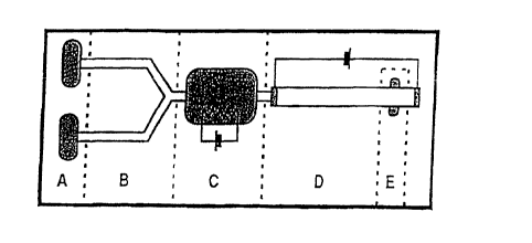
FIG. 1. Example of an integrated DNA analysis system, represented
schematically. The
individual components of the system are injection entry ports (A), liquid
pumping channels (B),
thermally (i. e. , isothermally) controlled reaction chamber (C),
electrophoresis channel (D), and
DNA band migration detector (E). Each component would have associated sensors,
control
circuitry, and external connections.
CA 02276251 1999-06-30
WO 98122625 PCT/US97121333
FIG. 2A and FIG. 2B. A two-part approach to construction of a silicon device
of the
present invention, and a silicon substrate comprising a plurality of devices.
FIG. 2A shows one
embodiment of a single microfluidic device. FIG. 2B shows one aspect of a
silicon device
comprising a plurality of microfluidic device modules.
5 FIG. 3A and FIG. 3B. A schematic of one embodiment of a device to split a
nanoliter-
volume liquid sample and move it using gas -from a gas source. FIG. 3A shows
the liquid
sample prior to splitting. FIG. 3B shows the liquid sample after splitting off
a microdroplet of
length L. The hatched regions represent the hydrophobic regions.
FIG. 4A and FIG. 4B. A schematic of one embodiment of a device of the present
10 invention to split, move and stop microdroplets using internal gas pressure
generation. FIG. 4A
shows a liquid sample prior to splitting. FIG. 4B shows the liquid sample
after splitting off a
microdroplet of length L. The hatched regions represent the hydrophobic
regions.
FIG. 5. Schematic drawing showing the principle of thermally induced drop
motion in a
closed channel. The case of a single aqueous drop in a hydrophilic channel is
presented, where
15 V is an applied voltage, Pe~m is atmospheric pressure, P2 is the receding-
edge internal pressure,
P2 is the advancing-edge internal pressure, and 8 is the contact angle of the
liquid-gas-solid
interface. The contact angle will depend on the surface characteristics of the
channel and the
constituents of the drop, with a hydrophilic interaction giving 8 between
0° and 90°, and a
hydrophobic surface giving 0 between 90° and 180°. Surface
treatments can also reduce contact
20 angle hysteresis and, therefore, reduce the temperature difference
necessary for drop motion.
DESCRIPTION OF ILLUSTRATIVE EMBODIMENTS
I. DESIGN OF MICROSCALE DEVICES FOR ISOTHERMAL AMPLIFICATION REACTIONS
25 The amplification of nucleic acids provides a convenient way to diagnose a
variety of
disease states. However, prior to the present invention, it was unknown
whether the movement,
mixing, and merging of viscous microvolume fluids at lower temperature to
conduct isothermal
amplification reactions was possible in a microfabricated environment.
Isothermal amplification
reactions employ reaction schemes and enzymes which are very different from
PCRTM, and it is
CA 02276251 1999-06-30
WO 98/22625 PCT/US97/21333
26
unknown whether or not the enzymology of isothermal amplification reactions is
compatible
with chip hardware and materials.
Specifically, the only enzyme necessary for PCRTM amplification of DNA targets
is a
thermostable DNA polymerise. Isothermal DNA amplification reactions employ
additional
enzymes with different biological activities because heat is not used to
denature double-stranded
nucleic acids. In addition to a DNA polymerise, 3 SR requires an enzyme with
RNase H activity
and an RNA polymerise. The SDA reaction requires several very specific
enzymatic activities
which are not necessary for PCRTM in order to successfully amplify a target
sequence. In
addition to synthesizing a new DNA strand, the DNA polymerise in SDA must lack
5'-3'
exonuclease activity, either naturally or by inactivation, incorporate the
modified nucleotides
required by SDA (athio-dNTPs or other modified dNTPs), and displace a
downstream single
strand from a double stranded molecule starting at a single stranded nick. In
addition, the
restriction endonuclease in SDA must nick (i. e., cleave a single strand of)
its double stranded
recognition/cleavage site when the recognition/cleavage site is hemimodified
and dissociate from
its recognition/cleavage site rapidly enough to allow the polymerise to bind
and amplify the
target efficiently. The restriction endonuclease must exhibit these activities
under reaction
conditions which are compatible with the activities required of the
polymerise.
It was not previously known if the enzymatic activities required for such
isothermal
amplification reactions would be inhibited by interaction with the surfaces of
silicon
microfabricated analysis devices or by inhibitors present in the devices
(e.g., residual chemicals
from microfabrication). In addition, the change in surface-to-volume ratio
which accompanies
taking an enzymatic reaction developed in a test tube to the microchannel of a
silicon
microfabricated device may have unpredictable effects, as changes in the
diffusion properties of
the reactants in the channel may interfere with the amplification reaction. In
particular for SDA,
the interaction of the derivatized dNTPs with the microdevice environment, the
effect of the
environment on nicking activity by the restriction endonuclease and strand-
displacing activity by
the polymerise were not known. It is known that liquid movement in a closed
channel, which is
a convenient means for bringing components of the amplification reaction into
contact, is
affected by the contact angle of the liquid-gas-solid interface within the
channel. Changes in the
composition of the liquid in the channel change the surface tension and
therefore the contact
angle, affecting liquid movement. The contact angle is reduced and liquid
movement is
CA 02276251 1999-06-30
WO 9$I226Z5 PCTILTS97/21333
27
facilitated by more hydrophilic liquids such as the reaction buffers
conventionally used in
PCRTM.
Certain isothermal amplification reactions, such as SDA, employ hydrophobic
components such as glycerol and BSA, which may unpredictably affect the
surface tension
properties of the liquid and the ability to move it within the channels of
microfabricated devices,
particularly when thermocapillary pumps are used. The need to increase the
amount of heat to
move the liquid aliquot with a thermocapillary pump could be incompatible with
the temperature
requirements of the enzymes and the isothermal amplification reaction.
Lowering the temperature of the amplification reaction may also have
unpredictable
effects. The temperature of the reaction in the microfabricated device is
typically controlled
from one side of the chip, setting up a temperature gradient across the
channel. The temperature
conditions of isothermal amplification reactions would also be expected to
alter the interactions
of the reactants with the silicon or glass surfaces of the channel. Because
isothermal
amplification is conducted at constant, lower temperatures, the temperature
gradient which is
produced reaches equilibrium and becomes stagnant. In contrast, the
temperature gradient in
higher temperature reactions with thermocycling is not stagnant. Temperature
fluctuations
during PCRTM amplification serve to minimize the gradient effect, improve
diffusion of reactants
and facilitate mixing.
Mixing of reactants in the channels and chambers of the DNA chip is of
particular
concern in isothermal amplification reactions, as mixing of reactants
initiates the amplification
reaction. This is not the case in PCRT"', as all reactants required for
amplification are present
together in the reaction mix. PCRTM amplification of double-stranded targets
does not begin
until temperature cycling is started because until that time no single-
stranded target is available
to amplify. This is not the case in isothermal amplification reactions.
Because strand separation
is an enzymatic process in isothermal amplification, at least one of the
enzyme reactants (usually
the polymerise) is withheld until it is desired to begin the reaction. If the
isothermal
amplification reaction starts with a heat-denaturation step and the enzymes
employed are not
thermostable, all of the enzymes for amplification are typically withheld
until the target-
containing sample is cooled to the appropriate reaction temperature. The
sample containing the
CA 02276251 1999-06-30
WO 98/22625 PCT/US97/21333
28
enzyme or enzymes must be mixed with the remaining reagents in order for
amplification to
begin.
To control initiation of the isothermal amplification reaction and provide an
integrated
nucleic acid analysis system, it is therefore highly desirable to keep the
components separate an
the microfabricated device and bring them together to initiate amplification.
This requires,
however, that mixing of the two components in the channel be adequate at the
lower
temperatures of isothermal amplification, and this mixing may be negatively
affected due to
temperature-related decreases in diffusion and changes in surface chemistry.
The components of
the amplification reaction itself may also have negative effects on mixing
within the channel.
Many amplification reactions contain reagents such as glycerol and bovine
serum albumin which
increase viscosity and could reduce mixing. The viscosity-increasing effects
of these reagents is
increased at lower temperatures. It was therefore unknown whether or not there
would be
adequate mixing, diffusion and temperature regulation to produce isothermal
amplification on a
silicon microfabricated device.
In certain aspects, the present invention relates to movement of microdroplets
through
microchannels, and more particularly, compositions, devices and methods to
control
microdroplet size and movement. The present invention involves
microfabrication of microscale
devices and reactions in microscale devices, and in particular, movement of
biological samples in
microdroplets through microchannels to, for example, initiate biological
reactions, particularly
isothermal amplification of nucleic acids.
Although there are many formats, materials, and size scales for constructing
integrated
fluidic systems, the present invention contemplates silicon microfabricated
devices as a cost-
effective solution.
The present invention contemplates microscale devices, comprising microdroplet
transport channels, reaction regions (e. g. , chambers), electrophoresis
modules, and radiation
detectors. In a preferred embodiment, these elements are microfabricated from
silicon and glass
substrates. The various components are linked (i. e., in liquid communication)
using a surface-
tension-gradient mechanism in which discrete droplets are differentially
heated and propelled
through etched channels. Electronic components are fabricated on the same
substrate material,
allowing sensors and controlling circuitry to be incorporated in the same
device. Since all of the
CA 02276251 1999-06-30
WO 98/22625 PCT/US97/21333
29
components are made using conventional photolithographic techniques, multi-
component
devices can be readily assembled into complex, integrated systems.
Continuous flow liquid transport has been described using a microfluidic
device
developed with silicon (Pfahler et al., 1990). Pumps have also been described,
using external
forces to create flow, based on micromachining of silicon (Van Lintel et al.,
.1988). The present
invention employs discrete droplet transport in silicon using internal forces
or external forces
{i.e., external forces created by pumps).
As a mechanical building material, silicon has well-known fabrication
characteristics.
The economic attraction of silicon devices is that their associated
micromachining technologies
are, essentially, photographic reproduction techniques. In these processes,
transparent templates
or masks containing opaque designs are used to photodefine objects on the
surface of the silicon
substrate. The patterns on the templates are generated with computer-aided
design programs and
can delineate structures with line-widths of less than one micron. Once a
template is generated,
it may be used almost indefinitely to produce identical replicate structures.
Consequently, even
extremely complex micromachines may be reproduced in mass quantities and at
low incremental
unit cost -- provided that all of the components are compatible with the
silicon micromachining
process. While other substrates, such as glass or quartz, can use
photolithographic methods to
construct microfabricated analysis devices, only silicon gives the added
advantage of allowing a
large variety of electronic components to be fabricated within the same
structure.
In one embodiment, the present invention contemplates silicon micromachined
components in an integrated analysis system, including the elements identified
schematically in
FIG. 1. In this proposed format, sample and reagent are injected into the
device through entry
ports (FIG. 1-A) and they are transported as discrete droplets through
channels (FIG. 1-B) to a
reaction chamber, such as an isothermally controlled reactor where mixing and
reactions, such as
isothermal nucleic acid amplification reactions (SDA, Q~i-replicase, etc),
restriction enzyme
digestion, ligation, phosphorylation, dephosphorylation, sequencing or other
enzymatic or
chemical reaction known to those of skill in the art occur (FIG. 1-C). The
biochemical products
are then moved by the same method to an electrophoresis module (FIG. 1-D)
where migration
data is collected by a detector (FIG. 1-E) and transmitted to a recording
instrument. Importantly,
CA 02276251 1999-06-30
WO 98/22625 PCT/US97/21333
the fluidic and electronic components are designed to be fully compatible in
function and
construction with the biological reactions and reagents.
A. Two-Part Approach to Construction
Most of the devices of the invention are hybrid micromechanical devices (two
substrates
5 bonded together). The purpose of using this method is to allow the
fabrication of
micromechanical devices out of a variety of materials (silicon, glass, fused
silica, quartz, etc.).
The devices have chamber volumes that are easily handled (sample loading,
component analysis,
etc.) and chamber walls that are transparent (sample loading, fluorescent
detection, etc.). The
hybrid system also gives flexibility in choosing materials in one section of
the unit without
10 affecting other pans of that same unit.
The invention may comprise two separate wafers of either the same or different
materials,
including but, not limited to, silicon, glass, or quartz are micromachined
independently. The
pieces are then bonded together using a variety-of techniques (polyimide, UV-
curing cements,
anodic bonding, etc.). For transparency, a glass or quartz wafer is usually
used on one side of the
15 hybrid. In general, the sensors, heaters, and other electronic components
may be patterned onto
one wafer and etch channels into the other. The electronic components may use
5 pm wire width
over channel regions so that, if the glass wafer has the electronic components
patterned on it, the
contents of the channels may be seen.
FIG. 2A shows a two-part approach to construction. Microchannels ( 100) are
made in the
20 silicon substrate (200) and the structure is bonded to a glass substrate
(300). The two-part
channel construction technique requires alignment and bonding processes but is
amenable to a
variety of substrates and channel profiles. In other words, for manufacturing
purposes, the two-
part approach allows for customizing one piece (i. e. , the silicon with
channels and reaction
formats) and bonding with a standardized (non-customized) second piece, e.g.,
containing
25 standard electrical pads (400):
Hundreds or thousands of copies of a particular component can be made
simultaneously
across the entire silicon wafer surface (FIG. 2B; for example, but not limited
to, a wafer that is
0.5 mm thick and 100 mm in diameter). The components are made by sequential
deposition, ion
implantation, or etching of thin layer materials in defined patterns.
Materials that are commonly
30 used include silicon oxide, silicon nitride, and various metals and alloys.
CA 02276251 1999-06-30
WO 98/22625 PCT/US97/21333
31
The technology of silicon fabrication is essentially a photolithographic
method for
making machines. Once a "template" or "stencil" pattern has been prepared,
additional copies of
the machines are replicated at minimal cost and effort. The density of
components is limited by
line-width considerations and the designing abilities of the engineers.
Complete devices are
made in batches and can often exceed thousands of replicates per fabrication
run. Additionally,
silicon fabrication has benefited from massive industrial commitment over the
past 20 years.
The characteristics of the fabrication steps are known and have been
incorporated into intelligent
design software or computer-aided design and manufacturing packages (CAD/CAM).
B. Channel Design and Construction
In silicon micromachining, a technique to form closed channels involves
etching an open
trough on the surface of a substrate and then bonding a second, unetched
substrate over the open
channel. There are a wide variety of isotropic and anisotropic etch reagents,
either liquid or
gaseous, that can produce channels with well-defined side walls and uniform
etch depths. Since
the paths of the channels are defined by the photo-process mask, the
complexity of channel
patterns on the device is virtually unlimited. Controlled etching can also
produce sample entry
holes that pass completely through the substrate, resulting in entry ports on
the outside surface of
the device connected to channel structures.
The present invention contemplates a variety of silicon-based, microdroplet
transport
channel-containing devices. In one embodiment, the device comprises: a housing
comprised of
silicon, a microdroplet transport channel etched in the silicon, a
microdroplet receiving means in
liquid communication with a reaction region via said transport channels, and a
liquid barrier
disposed between the transport channels and a microdroplet flow-directing
means. In one
embodiment, the device is assembled in two parts. First, the channels are
etched in any number
of configurations. Second, this piece is bonded with a silicon-based chip
containing the
electronics. This allows for both customization (in the first piece) and
standardization (in the
second piece).
In certain aspects of the invention "conveying" may refer to causing to be
moved through,
as in the case where a microdroplet is conveyed through a transport channel to
a particular point,
such as a reaction region. Conveying may be accomplished via a flow-directing
means.
CA 02276251 1999-06-30
WO 98!22625 PCT/US97/21333
32
The present invention also contemplates devices and methods for the sealing of
channels
with meltable material. In one embodiment, the device comprises a meltable
material disposed
within a substrate and associated with a heating element.
In one embodiment, the present invention contemplates a method comprising
providing a
device having a meltable material disposed within a substrate and associated
with a heating
element, and heating the meltable material with the heating element such that
the meltable
material at least partially liquefies and such that the substrate is not
damaged. The method may
further comprise allowing the liquefied meltable material to cool. While the
present invention is
not limited by the size of the channel, in one embodiment the substrate
further comprises a
microdroplet channel disposed in the substrate, the meltable material is
disposed within the
microdroplet channel.
In another embodiment, the present invention contemplates a method for
restricting fluid
flow in a channel comprising providing a device comprising a meltable material
disposed within
a substrate, the meltable material associated with a heating element; and a
diaphragm positioned
such that, when extended, it touches the meltable material, extending the
diaphragm such that it
touches the meltable material, and heating the meltable material with the
heating element such
that the meltable material at least partially liquefies and such that the
substrate is not damaged.
In one embodiment the method further comprises allowing the meltable material
to cool. While
the present invention is not limited by the size of the channel, in one
embodiment, the substrate
fiu ther comprises a microdroplet channel disposed in the substrate, the
meltable material
disposed within the microdroplet channel.
In certain aspects of the invention "meltable material" may refer to a
material that is at
least semi-solid (and preferably completely solid) at ambient temperature,
will liquefy when
heated to temperatures above ambient temperature, and will at least partially
resolidify when
cooled. Preferably, meltable material at least partially liquefies at a
temperature such that the
substrate is undamaged. That is to say, at the temperature the meltable
material liquefies, the
substrate and other metals in the substrate does not liquefy (readily tested
as set forth in
Example 6) and does not change its properties. By "changing properties" it is
meant that the
substrate or metal maintains it structural integrity, does not change its
conductivity and does not
CA 02276251 1999-06-30
WO 98/22625 PCTlUS97/21333
33
liquefy. Thus, the characteristic of being meitable is not necessarily
associated with a particular
melting point. Examples include, but are not limited to, solder, wax, polymer
and plastic.
In certain aspects of the invention "solder" may refer to a metal or alloy
that is a meltable
material. Preferably, the solder is a lower temperature solder, such as set
forth in U.S. Patent No.
4,967,950, herein incorporated by reference. "Lower temperature solder" means
a eutectic alloy.
While the present invention is not limited to a specific solder, one preferred
solder composition
for the paste is a 63:37 eutectic alloy of tin:lead. Another compatible solder
is a 90% metal
composition having a 63:35:2 eutectic alloy of tin:leadailver. Other desired
solder compositions
such as eutectic Pb:Sn, Pb:In, Pb:In:Sn, etc.
The present invention also contemplates a method for restricting fluid flow in
a channel,
comprising providing a main channel connected to a side channel and disposed
within a
substrate, meltable material disposed within the side channel and associated
with a heating
element, and a movement means connected to the side channel such that
application of the
movement means induces the meltable material to flow from the side channel
into the main
channel, heating the meltable material such that the meltable material at
least partially liquefies,
and applying the movement means such that the liquefied meltable material
flows from the side
channel into the main channel. While the present invention is not limited by
the movement
means, in one embodiment the movement means is forced air. In one embodiment
the method
further comprises allowing the meltable material to cool. While the present
invention is not
limited by the size of the channel, in one embodiment, the main channel and
the side channel are
microdroplet channels.
While the present invention is not limited by the nature of the substrate, in
one
embodiment the substrate comprises silicon or glass. Likewise, the present
invention is not
limited by the composition of the meltable material. In one embodiment, the
meltable material
comprises solder. In a preferred embodiment, the solder comprises 40:60 Sn:Pb.
In other
embodiments, the meltable material is selected from a group consisting of
plastic, polymer and
wax. Likewise, the present invention is not limited by the placement of the
meltabie material in
the substrate. In another embodiment, the meltable material is placed adjacent
to a channel,
while in another embodiment it is placed near the junction of more than one
channel.
CA 02276251 1999-06-30
WO 98/22625 PCT/US97/21333
34
II. MICROFABRICATION OF SILICON-BASED DEVICES
As noted previously, silicon has well-known fabrication characteristics and
associated
photographic reproduction techniques. The principal modern method for
fabricating
semiconductor integrated circuits is the so-called planar process. The planar
process relies on the
unique characteristics of silicon and comprises a complex sequence of
manufacturing steps
involving deposition, oxidation, photolithography, diffusion and/or ion
implantation, and
metallization, to fabricate a "layered" integrated circuit device in a silicon
substrate. See e.g.,
Miller, U.S. Patent No. 5,091,328, hereby incorporated by reference.
For example, oxidation of a crystalline silicon substrate results in the
formation of a layer
of silicon dioxide on the substrate surface. Photolithography can then be used
to selectively
pattern and etch the silicon dioxide layer to expose a portion of the
underlying substrate. These
openings in the silicon dioxide layer allow for the introduction ("doping") of
ions ("dopant") into
defined areas of the underlying silicon. The silicon dioxide acts as a mask;
that is, doping only
occurs where there are openings. Careful control of the doping process and of
the type of dopant
allows for the creation of localized areas of different electrical resistivity
in the silicon. The
particular placement of acceptor ion-doped (positive free hole, "p") regions
and donor ion-doped
(negative free electron, "n") regions in large part defines the interrelated
design of the transistors,
resistors, capacitors and other circuit elements on the silicon wafer.
Electrical interconnection
and contact to the various p or n regions that make up the integrated circuit
is made by a
deposition of a thin film of conductive material, usually aluminum or
polysilicon, thereby
finalizing the design of the integrated circuit.
Of course, the particular fabrication process and sequence used will depend on
the desired
characteristics of the device. Today, one can choose from among a wide variety
of devices and
circuits to implement a desired digital or analog logic feature.
In a preferred embodiment, channels were prepared on S00 pm thick glass wafers
(Dow
Corning 7740) using standard aqueous-based etch procedures. The initial glass
surface was
cleaned and received two layers of electron beam evaporated metal (20 nm
chromium followed
by 50 nm gold). Photoresist Microposit 1813 (Shipley Co.) was applied 4000
rpm, 30 sec;
patterned using glass mask 1 and developed. The metal layers were etched in
chromium etchant
CA 02276251 1999-06-30
WO .98/22625 PCT/US97121333
(Cr-14, Cyantek Inc.,) and gold etchant (Gold Etchant TFA, Transene Co.,)
until the pattern was
clearly visible on the glass surface. The accessible glass was then etched in
a solution of
hydrofluoric acid and water (1:1, v/v). Etch rates were estimated using test
wafers, with the final
etch typically giving channel depths of 20 to 30 p,m. For each wafer, the
depth of the finished
5 channel was determined using a surface profilometer. The final stripping
(PRS-2000, J.T. Baker)
removed both the remaining photoresist material and the overlying metal.
In one embodiment, channels etched on glass in the above-described manner,
were
bonded to the heater-element wafer in a two-part construction approach using
optical adhesive
(SK-9 Lens Bond, Sumers Laboratories, Fort Washington, PA). The bond was cured
under an
10 ultraviolet light source (365 nm) for 12 to 24 h.
Initial device design involved single layers of silicon. However, experience
showed these
to be inadequate to prevent short circuiting due to (necessary) liquid
microdroplets within the
channels (see studies described below). The preferred design involves a triple
layer of oxides.
Such a preferred device capable of moving and mixing nanoliter droplets was
constructed by
15 bonding a planar silicon substrate to channels etched in a glass cover. A
series of metal heaters
was inlaid on the silicon substrate as two parallel lanes merging into a
single lane (a "Y"-shape).
The heating elements were formed by first coating the wafer with a 1.0 pm
layer of thermal
silicon dioxide. Next, 0.35 p,m deep, S pm wide grooves were reactive-ion
etched {RIE) into the
silicon dioxide following the pattern set in an overlying photoresist.
Aluminum was deposited
20 (0.35 p,m) across the entire wafer using electron beam evaporation and the
metal layer was
"lifted-off' from all surfaces having intact photoresist using a stripping
solution. The metal inlay
process gives a relatively planar surface and provides a uniform base for
deposition of a solution-
impermeable barrier layer. The barrier layer is made by a sequence of three
plasma-enhanced
chemical vapor depositions (PECVD): 1.0 pm silicon oxide (SiOX), 0.25 ~m
silicon nitride
25 (SiXNy) and 1.0 pm silicon oxide (SiOX). Some heating elements were also
used as resistive
temperature sensors.
Heater elements were fabricated as follows. Silicon wafer (p-type, 18-22 '/2-
cm, boron
concentration ~ 1 O ~ 5 Cm 3) was used as a substrate for growth of Si02
thermal oxide ( 1 pm);
photoresist (AZ-5214-E, Hoescht-Celanese) was applied and spun at 3000 rpm, 30
sec. The
30 resist was patterned (metal 1 ) and developed. Reactive ion etch (RIE,
PlasmaTherm, Inc.) was
CA 02276251 1999-06-30
WO 98/22625 PCT/US97/21333
36
performed to 0.35 Pm depth into the Si02 layer at the following conditions:
CHF3, 15 sccm
(standard cubic centimeters per min); CF4, 15 sccm; 4 mTorr; DC bias voltage
of 200V, 100 W,
20 min. The etch depth was measured by profilometer and 0.35 pm metallic
aluminum was
electron beam deposited. The resist and overlying metal was lifted off by
development using
Microposit 1112A remover in solution (Shipley Co.,). The barrier layers
consist of sequentially
deposited 1 ~m SiOX, 0.25 ~m SiXNy, and 1 p,m SiOX using plasma-enhanced
chemical vapor
deposition (PECVD). RIE was used to etch contact holes to the metal layer
using a second mask
(CHF3, 15 scan; CF4, 15 seem; 4 mTorr; and DC bias voltage of 200V, 100 W, I20
min).
The elements are arrayed as two parallel lanes, each 500 ~,m wide, merging
into one lane.
The individual heaters consist of paired aluminum wires (5 ~,m) winding across
the 500 ~,m wide
region. The broad metal areas on either side of the elements are bonding
locations for
connection to external circuitry. The width of the aluminum element is 5 Vim.
The channel is
uniformly etched 500 Pm wide and approximately 20 ~m deep.
The heating-element wafer was bonded to a glass wafer containing etched
channels with
the same "Y" format. An aqueous chemical etch of concentrated hydrofluoric
acid was used to
produce channels with defined side walls and uniform depth. The etched
channels are defined by
a chromium/gold mask and are 500 ~m wide and approximately 20 ~,m deep. The
complementary silicon heater and glass channel wafers were aligned and then
bonded with
adhesive to form the finished device.
Each heating element used as a temperature sensor is preferably first
calibrated by
measurement of electrical resistance at 22°C and 65°C under
constant voltage; intermediate
temperatures are estimated by linear interpolation.
A. Microchannel Construction
There are two basic techniques that may be used for construction of channel
structures.
The first technique uses a chemical or a reactive ion etch to form open
channels on selected areas
of a substrate. These channels can range in width from 10 p,m to the full
thickness of the wafer
(500 Pm). The open channels are sealed by bonding of a second substrate as a
cap on top of the
first one. Common bonding techniques include anodic bonding, fusion bonding,
melting, and
epoxy bonding. Holes at specific locations for injection of the sample are
then etched from the
backside of the cap wafer. Bonded structures have been successfully applied in
the
CA 02276251 1999-06-30
WO 98122625 PCT/US97/21333
37
implementation of capillary liquid electrophoresis systems etched on glass
substrates (Burggraf
et al., 1993, ; Harrison et al., 1993). Most bonded structures are simple
discrete channel devices
with a limited number of electrical components and interconnects. However, the
bonded nature
of the device means that the substrate material containing the electrical
components may be
different than the cap material, adding great flexibility to device design.
The second technique for the fabrication of channels relies on the sacrificial
etch
technique (Mastrangelo and Muller 1989). In this technique, the channel is
formed from a
patterned thin film that determines the channel height. The film is covered by
the deposition of a
thick cap material and access holes are opened through it. The sacrificial
material defining the
channel is next removed by chemical etching through the access holes, and
finally the channel is
sealed by plugging the access holes. The main advantage of this fabrication
approach is that the
channel fabrication takes place entirely on one side of the substrate; hence
this technique is
referred as surface micromachining. The ability to pattern channels on the
surface of the
substrate brings a great deal of flexibility. Surface micromachined channels
may be fabricated
on substrates with complex topographies of interconnects, sensors, and control
electronics. In
surface micromachined devices, the analytical instrumentation is built along
with the channel on
the same physical substrate.
The devices by both the hybrid (bonded) and monolithic (surface machining)
designs
have been constructed. For bonded structures, both glass and silicon
substrates to form channels
(500 pm wide), and t-circuits (aluminum heater circuitry, each wire filament
is 5 p,m wide) have
been used. The monolithic device is compatible with conventional NMOS device
fabrication.
B. Channel Fabrication
The channels are made of diffused silicon on the bottom and a thin film cap on
the top.
This type of channel may be routed through low-mass diaphragm-type heaters
needed for the
reaction. On the top layer, a set of thin film electrodes and heaters is
constructed. Both the
channels and entry port components can be formed by etching of silicon. The
depth of etching
can be controlled by prior doping of the silicon material with an etch stop
(boron).
The surface treatment of the channels may be done by immersing the open
channel in
organosilane or a self assembled monolayer coating, with oxygen reactive ion
etching removing
the surface from unwanted areas: Heating elements, dielectric sensors, and
connecting wires
CA 02276251 1999-06-30
WO 98/22625 PCT/US97/21333
38
may be made from sputtered aluminum metal and conventional masking. The
sequential
activation of heating elements can be computer controlled through external
circuitry, and a
printed circuit board connector.
C. Channel Treatment
Prior to performing microdroplet motion and biological reactions, the channels
are
preferably treated by washing with base, acid, buffer, water and a
hydrophilicity-enhancing
compound, followed by a relatively high concentration solution of non-specific
protein.
"Hydrophilicity-enhancing compounds" are those compounds or preparations that
enhance the
hydrophilicity of a component, such as the hydrophilicity of a transport
channel. The definition
is functional, rather than structural. For example, Rain-XTM anti-fog is a
commercially available
reagent containing glycols and siloxanes in ethyl alcohol. However, the fact
that it renders a
glass or silicon surface more hydrophilic is more important than the reagent's
particular formula.
"Hydrophobic reagents" are used to make "hydrophobic coatings" in channels. It
is not
intended that the present invention be limited to particular hydrophobic
reagents. In one
1 S embodiment, the present invention contemplates hydrophobic polymer
molecules that can be
grafted chemically to the silicon oxide surface. Such polymer molecules
include, but are not
limited to, polydimethylsiloxane. In another embodiment, the present invention
contemplates the
use of silanes to make hydrophobic coatings, including but not limited to
halogenated silanes and
alkylsilanes. In this regard, it is not intended that the present invention be
limited to particular
silanes; the selection of the silane is only limited in a functional sense,
i.e., that it render the
surface hydrophobic.
In various aspects of the invention, n-octadecyltrichlorosilane (OTS),
octadecyldimethylchlorosilane, 1 H, 1 H, 2H, 2H-perfluorodecyltricholorosilane
(FDTS,
CloH4F~~SiCl3), fluoroalkyl-, aminoalkyl-, phenyl-, vinyl-, bis silyl ethane-
or
3-methacryloxypropyltrimethoxysilane (MAOP) are contemplated as hydrophobic
reagents.
Such reagents (or mixtures thereof) are useful for making hydrophobic
coatings, and more
preferably, useful for making regions of a channel hydrophobic (as distinct
from coating the
entire channel).
In a preferred embodiment, the channels are washed with approximately 100 p,l
each of
the following solutions in series: O.1N NaOH; O.1N HCI; 10 mM Tris-HCl (pH
8.0), deionized,
CA 02276251 1999-06-30
WO 98/22625 PCT/US97/21333
39
H20, Rain-~ Anti-Fog (a hydrophilicity-enhancing compound commercially
available from
Unelko Corp., Scottsdale, AZ), and 500 p,g/pl bovine serum albumin (non-
specific protein
commercially available in restriction enzyme grade from GIBCO-BRL). The wafer
was placed
on a stereoscope stage (Olympus SZ1145), and the contact pads for the heating
elements were
connected to a regulated power supply. Heating occurred by passing
approximately 30 volts
through the element in short pulses and observing the movement rate of the
droplets. A
detectable reduction in droplet volume from evaporation was noted in each
study, usually of less
than 30%. Droplet movement was recorded with a Hamamatsu video camera on
videotape.
It is not intended that the present invention be limited to particular
dimensions for the
hydrophobic regions of the present invention. While a variety of dimensions
are possible, it is
generally preferred that the regions have a width of between approximately 10
and 1000 pm (or
greater if desired), and more preferably between approximately 100 and 500 pm.
A surface (such as a channel surface) is "hydrophobic" when it displays
advancing
contact angles for water greater than approximately seventy degrees. In one
embodiment, the
treated channel surfaces of the present invention display advancing contact
angles for water
between approximately ninety (90) and approximately one hundred and thirty
(130) degrees. In
another embodiment, the treated microchannels have regions displaying
advancing contact
angles for water greater than approximately one hundred and thirty ( 130)
degrees.
D. Glass Channel and Chamber Fabrication
The channel and the chamber fabrication begins by depositing 0.4 pm metallic
layer of
Gold (Electron beam deposition) on the surface of S00 ~m thick glass water
(Dow Coming
7740). A 0.06 p.m layer of chromium is used as the adhesion layer. Photoresist
is applied and
patterned using glass mask 1 and developed. The metal layers are etched in
gold etchant (Gold
Etchant TFA, Transene Co.) and Chromium etchant (CR-14, Cyantec Inc.). The
accessible glass
is then etched in a solution of freshly prepared hydrofluoric and nitric acid
(7:3, v/v). The etch
rate is approximately Spm/min and the etch depth is conveniently measured
using a surface
profilometer. The metal layers are removed and the wafer rinsed in DI water,
air dried and oven
dried at 100°C for 20 min. The following processing-steps are done for
patterning hydrophobic
regions onto the glass surface.
CA 02276251 1999-06-30
W0.98/22625 PCT/US97/21333
1. Hydrophobic Patterning of Glass Substrate
A 1.5 pm thick aluminum layer was electron beam deposited, covering the etched
channels and chamber. A thick photoresist (AZ 4620) is applied and spun at 750
rpm for 50 sec .
The resist is patterned (SAM Mask) and developed. The exposed aluminum is
etched in
5 aluminum etchant. The photoresist is stripped off in hot PRS 2000 (J.T.
Baker). The samples
are then cleaned in acetone, isopropyl alcohol and DI water for 5 min each and
the water dried
off in a 100°C oven of 10-15 min. The samples are then dipped in a 1%
OTS solution in toluene
for 10-15 min. The SAM deposition was carried out in a chemical hood. The
samples were then
rinsed in toluene, isopropyl alcohol and DI water for 5 min each. Next, they
were put in
10 aluminum etchant until all metallic aluminum was removed. The samples were
then rinsed in DI
water and air dried. For the devices with the inlet from the top, holes were
drilled by
electrochemical discharge drilling.
The glass side was then aligned on top of the silicon side and then bonded
together using
optical adhesive (SK-9 Lens Bond, Sumers Laboratories, Fort Washington, PA).
The bond was
15 cured under an ultraviolet light source (365 nm) for 24 h.
E. Heaters and Resistive Temperature Detectors
The fabrication process for the heater and temperature detector begins by
using Silicon
water (p-type, 18-22 alun-cm, boron concentration --1 O15 cm3) as a substrate
for growth of S 102
thermal oxide ( 1 pm). A 0.5 ~.m metallic Aluminum film is electron beam
deposited.
20 Photoresist PR 1827 is applied and spun at 4000 rpm for 30 sec, patterned
(metal 1 ) and
developed. The exposed aluminum is etched in aluminum etchant and the
photoresist stripped to
define the metal heater.
Photoresist is spun again and a second lithography is done (metal 2). A 0.15
~m layer of
platinum ("Pt") is electron beam deposited. A 0.03 pm thick titanium metal
layer (electron beam
25 deposited) is used as the adhesion layer. The resist and the overlying
metal is lifted off by
development using Microposit 1112A remover in solution (Shipley Co.). This
platinum metal
will be used as the resistive thermal detector. Next, 0.7 pm of low
temperature oxide (LTO) of
silicon is deposited to act as the barrier layer and the hydrophilic
substrate. A third lithography
is done and the LTO is etched in buffered hydrofluoric acid to open contacts
to the metal contact
CA 02276251 1999-06-30
WO 98/22625 PCT/US97/2I333
41
pads. The further processing steps are done to pattern hydrophobic regions
onto the hydrophilic
silicon oxide surface.
1. Hydrophobic Patterning of Silicon Oxide Substrate
A 0.1 ~m layer of chromium metal is electronbeam deposited on the processed
water.
Photoresist PR 1827 is applied and spun at 2000 rpm for 30 sec. The resist is
patterned (SAM
mask) and developed. The exposed chromium metal is etched in chromium etchant
to expose the
silicon oxide and the photoresist is then stripped off. The samples are then
cleaned in acetone,
isopropyl alcohol and DI water for 10 min each, air dried and oven dried at
100°C for 5 min.
The samples are then put in 1 wt% octadecyltrichlorosilane (OTS) solution in
toluene for
15-30 min. OTS deposits on the samples as a self assembled monolayer (SAM).
The samples
are then rinsed in toluene, isopropyl alcohol and DI water for 5 min each, and
then oven dried
( 100°C, 5 min). Next, they are put in chromium etchant to remove the
chromium layer below.
The SAM on the chromium metal gets lifted off as a result of this. The samples
were then rinsed
in DI water and air dried, resulting in regions of intact hydrophobic regions
on a hydrophilic
oxide substrate. Heater elements and RTDs have also been fabricated on a
quartz substrate. The
fabrication steps are similar to that of the silicon processing steps.
Once the appropriate chemicals are added to the DNA sample, the solution may
be passed
through several different temperatures. The mixed solution may be transported
to a uniformly
heated reaction chamber of the unit. Once in the chamber, the temperature of
the solution may
be increased using local heaters and temperature sensors. The temperature of
the ends of the
drops may be monitored and maintained at the same temperature to prevent the
drop from
leaving the reaction zone. If the drop does begin to move, local temperature
gradients could
quickly stabilize the drop. The cooling of the drop may be accomplished by
simple conduction
of the heat through the walls of the channel to ambient temperature.
F. Fluid Mixing Chamber
The mixing chamber consists of an enlarged portion of the microchannel
structure, with
one or more microchannels connected to the chamber. The mixing chamber is
suspended on a
thin silicon nitride diaphragm. This construction allows for excellent thermal
isolation, as
needed for low power heat cycling of the mixture. Construction of membrane
suspended
structures has been demonstrated (Mastrangelo et al., 1991 ): The heating is
effected with a set of
CA 02276251 1999-06-30
W0 98/22625 PCT/US97/21333
42
concentric resistors (heaters) that are placed on the periphery of the mixing
chamber. This
design, along with the high thermal conductivity of the liquid sample, makes
the chamber
temperature quite uniform. Along with the heaters, temperature sensors
(diodes) are constructed
on the diaphragm to monitor the temperature of the mixture. The low mass
construction of the
chamber allows for rapid heating cycles. Temperature control may handle
samples of variable
volume and heat capacity. The chamber also contains a set of electrodes and
heating elements to
drive the mixture out of the chamber at the completion of the reaction.
G. Electrophoresis and Detector Component Design
The present invention contemplates one or more gel electrophoresis modules as
a
component of the microscale device. Reducing the thickness of the
electrophoresis channel may
improve resolution. Thinner gels dissipate heat more readily and allow higher
voltages to be
used, with concomitant improvements in separation. The position and width of
the
electrophoresis detector are also critical to the ultimate resolution of the
electrophoresis system.
A micromachined electronic detector, such as a photodiode, placed in the
underlying silicon
1 S substrate may be less than one micron from the gel matrix and can have a
width of 5 microns or
less. Since the gel length required for the resolution of two migrating bands
is proportional to
the resolution of the detector, the incorporation of micron-width electronic
detectors can reduce
the total gel length required for standard genotyping by at least an order of
magnitude.
To demonstrate that standard gel electrophoresis can operate in micron-
diameter
channels, modules were fabricated using etched glass channels and fluorescent-
labeled DNA
(YOYO intercalating dye). Polyacrylamide gel electrophoresis of a complex DNA
mixture was
performed in a channel 500 ~,m wide and 20 p,m deep. The electrophoresis was
performed with
the positive electrode to the right and the DNA sample applied at the left.
The DNA sample
(Bluescript KS digested with MspI) is labeled with intercalating tJV-
fluorescent dye (YOYO-1)
and is visualized under incandescent light. Separation of the component bands
is clearly visible
less than 300/p.m from the buffer reservoir-to-gel interface. The high
resolution of the detector
(in this case, a microscope) allowed the use of an unusually short gel,
resolving several closely
eluting bands.
CA 02276251 1999-06-30
WO 98122625 PCTIUS97/2I333
43
H. Miniature Electrophoresis Chamber
A 20 ~m x 500 p,m x 4 cm channel etched into a glass wafer was used as an
electrophoresis chamber. The channels may be made by three different
processes: a glass
channel wet-etched, a silicon channel dry-etched (RIE), or a silicon channel
wet-etched.
Although the edges of the channel are rough and the walls of the channels are
not vertical, the
floor of the channel is quite smooth. Better channels may also be constructed
with silicon as the
base material using dry or wet etching. The glass channel was then bonded to a
quartz slide
using L1V-cure cement and loaded with a 15% polyacrylamide gel and 1 x TBE
running buffer.
The gel was loaded with DNA ladder (BSKS/MSPI SO-500 bp), stained with TOTO
fluorescent
dye, and placed in a ~3 volt/cm field for 30 minutes. At these short times and
low voltages,
separation into visibly resolved bands is obtained.
I. Integrated Electrophoresis/Detection Device
Monolithic devices created from silicon have the advantage that no bonding is
necessary
and that electronic components may be integrated with the mechanical system in
any location. A
silicon micromachined gel electrophoresis channel integrated with a silicon
radiation/fluorescence detector underneath it was fabricated. The "die"
measures 1.25 x 1.25 cm
and contains about 20 different types of gel devices. Among these devices, the
channel width
varies from 20 to 150 Vim, and the channel height is approximately 3 p,m.
There are different
channel formats including straight, folded, and looped channels, each of which
has at least one
DNA detector. The longest channel on this wafer is a 9.5 cm long folded
channel. For folded
channels, as long as the channel bends are paired curves, it may be shown that
the electric field is
uniform around the bend and the solute bands start and end as uniform bands.
The structure primarily comprising a silicon diffused diode detector (Kemmer,
1980;
Wouters and van Sprakelaar 1993) fabricated underneath a gel channel. The
diode is fabricated
on a high purity p-type float zone substrate to assure a good carrier
lifetime. A layer of silicon
dioxide is used as a passivation layer below a silicon nitride blocking layer.
The electrodes for
the electrophoresis stage are formed by deposition and patterning of
n+polycrystalline silicon.
The channel for the microgel is built with two layers of phosphoslicate glass
as described in
Mastrangelo and Muller 1989; Mastrangelo and Muller 1989. The cap of the
channel is
deposited using a thin silicon nitride dielectric and a 2 m-thick undoped
polysilicon shell. A
series of etching holes are patterned on the side or top of the shell down to
the phosphosilicate
CA 02276251 1999-06-30
W0.98/22625 PCT/LJS97/21333
44.
glass and used to sacrificially etch the phosphosilicate glass (Mastrangelo
and Muller, 1989) thus
forming the channel cavity. The cavity can then be refilled with
polyacrylamide gel.
The invention has tested the radiation/fluorescence detectors and performed
simple DNA
separations with them. The experiments were performed using a P32 labeled DNA
source placed
on top of the detector. Note that the chip used for this test did not have the
channels formed on
the surface and contained as an insulating layer. Pulse-shaped (Knoll, 1989)
scope traces or the
measured signals from the diode detector were detected from sample DNA. Not
only is the
response rapid (~ 1 ps), but a single decay event (each trace is from only one
particle) may be
detected.
Fluorescent DNA may also be detected with the same detector. A detector was
mounted
in a 24 pin IC package and covered with a SYBR green gel filter (the filter
was ~l cm from the
detector surface). A glass slide was placed over the filter and ~40 p.l of
0.03 pg/pg of SYBR
green labeled DNA solution was placed on the slide (contained by silicon
grease wells). The
sample was illuminated using a Ziess Axioskop UV source with a 490 nm filter.
The reverse
current was measured with an HP 4145B semiconductor parameter analyzer as a
function of the
bias voltage. The signal from the SYBR sample is approximately twice the
control signal (DI
water). Although this experiment was not performed under optimum conditions,
it clearly
demonstrates that the detector is capable of detecting fluorescent DNA.
Sample separation experiments have also been performed using this detector. A
100 ~.m
ID capillary tube filled with 10% polyacrylamide was glued on top of a
detector (same as that
described above) approximately 1.5 cm from the sample injection end. A 100 by
and a 300 by
PCRTM product {50/50 mixture) was electrokinetically injected into the channel
for
approximately 5 min using a field of 25 V/cm after which the sample well was
flushed and
refilled with running buffer. The results of the 125 minute run show the
detection of the
radioactive primers and the two PCRTM products. Note that, although the
radiation detection
scheme may not be used in the final sequencing system, it is very useful to
evaluate the
electrophoresis chambers until the necessary, fluorescent filters are
constructed and tested.
The present invention contemplates an electrophoresis unitthat integrates a
micromachined channel and an electronic DNA detector. The channel is
constructed using a
sacrificial etch process on a single silicon wafer rather than the bonded
surface-etch method
CA 02276251 1999-06-30
WO 98!22625 PCT/US97/21333
described earlier. In the sacrificial etch technique, the channel
configuration is patterned by
depositing on the wafer surface an etch-sensitive material (phosphosilicate
glass, Si02 ~ PX) with a
thickness equivalent to the desired channel height. A triple-layer overlay of
plasma-enhanced
chemical vapor deposited silicon nitride, undoped. polycrystalline silicon,
and silicon nitride
5 (SiXNy/polySi/SiXNy) completely covers the sacrificial material with the
exception of small
access holes on the top or sides. A selective liquid etch removes the
sacrificial layer material,
but not the overlay or the underlying substrate. The sacrificial etch
technique results in a
complete channel being formed directly on the substrate containing the
electronic components.
The 3 p,m deep channel has two buffer reservoirs on either end with integral
phosphorus-doped
10 polycrystalline silicon electrodes. The channel height formed by this
technique (~3/pm) is
considerably smaller than the height of the bonded structures due to the
limitations of the
sacrificial layer deposition and the strength of the overlying layer. Note
that, for these channel
dimensions, liquid drops would have volumes on the order of picoliters.
The diffusion regions of the doped-diffusion diode radiation detector elements
fabricated
15 on a silicon wafer are approximately 300 pm long and 4 pm wide, and are
flanked by the guard
ring shielding electrodes.
A radiation detector, consisting of a 10 p.m wide "p-n"-type diode with a 5 pm
wide
guard ring around the outer edge, is fashioned directly into the silicon
substrate underneath the
channel. In this implementation, an integral radiation detector was chosen
because of high
20 sensitivity (a single decay event), small aperture dimensions, and well-
know fabrication and
response characteristics. On this electrophoresis system, a 1 cm long, 3 pm
thick gel is able to
perform as separation on a 80 and a 300 base-pair fragment of DNA. It should
be noted that this
diode, although currently configured for high-energy beta particle detection,
can also operate as a
photon detector. With proper wavelength filters and light sources, detection
of fluorescence
25 emission may be accommodated with a similar device.
Radiation detectors were prepared as follows. A 200 '/2-cm, float zone, boron-
doped,
p-type silicon wafer was used as a substrate. Diffused layers of phosphorus (5
x 104 cm 2) and
boron ( 1 x 10 ~ 5 cm 2) were ion-implanted onto the sample in
lithographically-defined regions;
thermal silicon oxide was grown (0.2 ~.m at 900°C) over the wafer; and
contact holes were
30 etched to the diffusion layer using buffered hydrofluoric acid solution
(5:1 ). A 3.3 pm layer of
CA 02276251 1999-06-30
WO 98/22625 PCT/L1S97/21333
46
Microposit 1400-37 photoresist was patterned to define the metal pads; 50 nm
chromium
followed by 400 nm gold was evaporated over the resist; and the metallization
lifted off the
regions retaining the resist. A layer of Microposit 1813 photoresist was
applied across the wafer
and baked for 110°C for 30 min to form an aqueous solution barrier.
Radioactive phosphorus
S (32P) decay events could be detected using a sample of labeled DNA in PCRTM
reaction buffer
placed on the photoresist layer. The detector was connected to a charge-
sensitive preamplifier
(EV-Products SSOA), followed by a linear shaping amplifier and a standard
oscilloscope.
An oscilloscope trace of output from the radiation detector showing individual
decay
events from 32P-labeled DNA was generated after the aqueous DNA sample was
placed directly
on the detector and sampled for 30 sec. The screen is displaying a vertical
scale of O.SV/division
and horizontal scale of 20 p,sec/division.
J. Gel Voltage and Temperature Control Circuits
The control circuitry and software for the integrated DNA sample processing
and -
sequencing devices are a further aspect of the invention. In particular, the
devices will require
circuitry for signal buffering and for the multiplexing of control signals. A
microprocessor,
either external or on-wafer, determines the synchronization of events on the
device and store the
output information.
Temperature control of gel occurs by heating with polysilicon or thin metal
resistors
imbedded in the surface of the wafer immediately beneath the channel. The
precise temperature
control of the gel is required as minute fluctuations contribute to the
dispersion of the migrating
sample and non-uniform bands. The power distribution and optimal heater
placement is
determined for each electrophoresis design by solving the relevant heat
transfer equations. As
long as the walls of the electrophoresis channel are maintained at the
appropriate temperature and
the height of the channel is constructed uniformly, the internal temperature
of the across the gel
should not vary by more than 1.0°C and be maintained at any arbitrary
temperature.
Although the electrophoresis voltages may be low, the potential use of high
voltages in
the gel electrophoresis channels will necessitate care in fabricating the
silicon oxide/silicon
nitride/silicon oxide insulating layer. Silicon nitride and silicon oxide have
a breakdown field
voltage of about 200-1000 V/p,m (Sze, 1967; Harari, 1977; Sze, 1981 ).
Consequently, the layers
between the silicon circuitry (including the diode detectors) and the
electrically active gel are
CA 02276251 1999-06-30
WO 98/22625 PCT/US97/21333
47
approximately 2 to 4 microns thick. The possible presence of minute "pinholes"
in the LPCVD
deposited layers must also be carefully monitored, since such holes can
provide local weak
points in the insulation of the silicon circuitry. However, the routine use of
silicon nitride as a
mask for wet etch processes in solid-state fabrication indicate that pinholes
are insignificant.
Glass may be used as their substrate material. In a glass-based device, any
associated on-
wafer circuitry must be constructed on polysilicon thin films adjacent to the
electrophoresis
channels (Tickle, 1969). As an alternative are designs that energize small
fractions of the
channel at a time, thereby decreasing the voltage required without sacrificing
resolution.
Cyclical or "loop" 9.5 cm channels were constructed to test this {Sun and
Hartwick, 1994).
However, since active electrodes are in immediate contact with the get matrix
care must be
exercised so as not to irreversibly adsorb the DNA samples on the electrodes.
Alternative gel
channel designs are possible.
In one embodiment of the device of the present invention, the device comprises
a glass
top bonded to a silicon substrate containing the heater, the contact pad and
the resistive
temperature detector. The glass side has channels and chambers etched into it.
Inlet and
overflow ports, a gas vent and a air chamber are also part of this embodiment.
III. FLUID MOVEMENT
The present invention contemplates a method for moving microdroplets,
comprising
providing a liquid microdroplet disposed within a microdroplet transport
channel etched in
silicon, the channel in liquid communication with a reaction region via the
transport channel and
separated from a microdroplet flow-directing means by a liquid barner, and
conveying the
microdroplet in the transport channel to the reaction region via the
microdroplet flow-directing
means. It is intended that the present invention be limited by the particular
nature of the
microdroplet flow-directing means. In one embodiment, it comprises a series of
aluminum
heating elements arrayed along the transport channel and the microdroplets are
conveyed by
differential heating of the microdroplet by the heating elements.
It has been found empirically that the methods and devices of the present
invention may
be used with success when, prior to the conveying described above the
transport channel (or
channels) is treated with a hydrophilicity-enhancing compound. It is not
intended that the
CA 02276251 1999-06-30
WO 98/22625 PCT/US97/21333
48
invention be limited by exactly when the treatment takes place. Indeed, there
is some flexibility
because of the long-life characteristics of some enhancing compounds.
It has also been found empirically that the methods and devices of the present
invention
may be used with success when regions of the microchannel are treated with
hydrophobic
reagents to create hydrophobic regions. By using defined, hydrophobic regions
at definite
locations in microchannels and using a pressure source, one can split off
precise nanoliter
volume liquid drops (i. e. , microdroplets) and control the motion of those
drops though the
microchannels.
In one embodiment employing such hydrophobic regions (or "hydrophobic
patches"), the
present invention contemplates a method for moving microdroplets, comprising
providing
microdroplet transport channel (or a device comprising a microdroplet
transport channel), the
channel having one or more hydrophobic regions and in communication with a gas
source;
introducing liquid into the channel under conditions such that the liquid
stops at one of the
hydrophobic regions so as to define a source of liquid microdroplets disposed
within the channel
and a liquid-abutting hydrophobic region, and separating a discrete amount of
liquid from the
source of liquid microdroplets using gas from the gas source under conditions
such that a
microdroplet of defined size comes in contact with, and moves over, the liquid-
abutting
hydrophobic region.
In one embodiment, the gas from the gas source enters the channel from a gas-
intake
pathway in communication with the microdroplet transport channel and exits the
channel from a
gas vent that is also in communication with the microdroplet transport
channel. It is preferred, in
this embodiment, that the introduction of liquid into the channel (as set
forth in the above-
described method) is such that the liquid passes over the gas-intake pathway
and the desired size
of the microdroplet is defined by the distance between the gas-intake pathway
and the liquid-
abutting hydrophobic region. In this embodiment, introduction of the gas (as
set forth in the
above-described method) forces the microdroplet to pass over the liquid-
abutting hydrophobic
region and pass by (but not enter) the gas vent.
In another embodiment employing such hydrophobic regions (or "hydrophobic
patches"),
the present invention contemplates a method for moving microdroplets,
comprising: providing a
device comprising a microdroplet transport channel etched in silicon, the
channel having one or
CA 02276251 1999-06-30
WO 98/22625 PCT/US97/21333
49 w
more hydrophobic regions and in communication with a gas source; introducing
liquid into the
channel under conditions such that the liquid stops at one of the hydrophobic
regions so as to
define a source of liquid microdroplets disposed within the channel and a
liquid abutting
hydrophobic region, and separating a discrete amount of liquid from the source
of liquid
microdroplets using gas from the gas source under conditions such that a
microdroplet of defined
size comes in contact with, and moves over, the liquid-abutting hydrophobic
region.
Again, it has been found empirically that there is a need for a liquid barner
between the
liquid in the channels and the electronics of the silicon chip. A preferred
barrier comprises a first
silicon oxide layer, a silicon nitride layer, and a second silicon oxide
layer.
The present invention further contemplates a method for merging microdroplets
comprising providing first and second liquid microdroplets, a liquid
microdroplet delivering
means, and a device, said device comprising a housing comprised of silicon,
first and second
microdroplet transport channels etched in the silicon and connecting to form a
third transport
channel containing a reaction region, a microdroplet receiving means in liquid
communication
1 S with the reaction region via the transport channels, and microdroplet flow-
directing means
arrayed along the first, second and third transport channels delivering the
first liquid
microdroplet via the microdroplet delivering means to the first transport
channel, delivering the
second liquid microdroplet via the microdroplet delivering means to the second
transport
channel, and conveying the microdroplets in the transport channels to the
reaction region in the
third transport channel via the microdroplet flow-directing means, thereby
merging the first and
second microdroplets to create a merged microdroplet.
In one embodiment, said first microdroplet comprises nucleic acid and the
second
microdroplet comprises a nuclease capable of acting on the nucleic acid. In
this embodiment, it
is desirable to enhance the mixing within the merged microdroplet. This may be
achieved a
number of ways. In one embodiment for mixing, after the conveying of step, the
flow direction
is reversed. It is not intended that the present invention be limited by the
nature or number of
reversals. If the flow direction of the merged microdroplet is reversed even a
single time, this
process increases the mixing of the reactants.
The present invention contemplates methods, compositions and devices for the
creation
of microdroplets of discrete (i. e., controlled and predetermined) size. The
present invention
CA 02276251 1999-06-30
W0 98122625 PCT/US97/Z1333
$0
contemplates the use of selective hydrophobic coatings to develop a liquid-
sample injection and
motion system that does not require the use of valves. In one embodiment, the
present invention
contemplates a method of lift-off to pattern hydrophobic and hydrophilic
regions on glass, quartz
and silicon substrates, involving the deposition of a hydrophobic reagent
(such as a self
assembled monolayer film of OTS) on a silicon oxide surface pattered by a
metal layer and
subsequent removal of the metal to give hydrophobic patterns. Other substrates
such as plastics
may also be used after depositing a think film of silicon oxide or spin-on-
glass.
Previous work in patterning hydrophobic surfaces have been done by
photocleaving of
such monolayer films. The photocleaving procedure uses Deep-UV exposure to
make the
molecules of the monolayer hydrophilic. By contrast, the present invention
contemplates a
method which eliminates the use of high-power UV source; rather the preferred
method of the
present invention uses microfabrication procedures.
Following the proper hydrophobic patterning of the surface (e.g., the surface
of a
microdroplet transport channel), the present invention contemplates the
placement of a patterned
etched glass cap over the pattern on a flat surface. The
hydrophobic/hydrophilic channels thus
formed can then be used to move precise nanoliter-volume liquid samples.
FIG. 3A and FIG. 3B show a schematic of one embodiment of a device (10) to
split a
nanoliter-volume liquid sample and move it using external air, said device
having a plurality of
hydrophobic regions (hatched regions). Looking at FIG. 3A, liquid {shown as
solid black)
placed at the inlet (20) is drawn in by surface forces and stops in the
channel at the liquid-
abutting hydrophobic region (40), with overflow handled by an overflow channel
and overflow
outlet (30). In the embodiment shown in FIG. 3A, the from of the liquid moves
by (but does not
enter) a gas-intake pathway (SO) that is in fluidic communication with the
channel; the liquid-
abutting hydrophobic region (40) causes the liquid to move to a definite
location. Gas from a gas
source (e. g. , air from an external air source and/or pump) can then be inj
ected (FIG. 3 B, lower
arrow) to split a microdroplet of length "L". The volume of the microdroplet
split-off (60) is pre-
determined and depends on the length "L" and the channel cross-section. To
prevent the pressure
of the gas (e.g., air) from acting towards the inlet side, the inlet (20) and
overflow ports (30) may
be blocked or may be loaded with excess water to increase the resistance to
flow.
CA 02276251 1999-06-30
WO 98/22625 PCT/US97/21333
51
The patterned surfaces may also be used to control the motion of the drop. By
placing a
hydrophobic gas vent (70) further down the channel, one can stop the liquid
microdroplet (60)
after moving beyond the vent (70). As the drop (60) passes the vent (70), the
air will go out
through the vent (70) and will not push the drop further.
One can start moving the drop (60) again by blocking the vent (70). By using a
combination of hydrophobic air pressure lines, hydrophobic vents and strategic
opening and/or
closing of vents, one can move the liquid drop back and forth for mixing or
move it to precise
locations in a channel network to perform operations such as heating, reaction
and/or separations.
In addition to using external air, one can also use internally generated air
pressure to split
and move drops. FIG. 4A and FIG. 4B show a schematic of one embodiment of a
device (110)
of the present invention to split (e.g., define), move and stop microdroplets
using internal gas
(e.g., air) pressure generation, said device having a plurality of hydrophobic
regions (hatched
regions). Looking at FIG. 4A, liquid (shown as solid black) placed at the
inlet (120) is drawn in
by surface forces and stops in the channel at the liquid-abutting hydrophobic
region ( 140), with
overflow handled by an overflow channel and overflow outlet {130). In the
embodiment shown
in FIG. 4A, the front of the liquid moves by {but does not enter) a gas-intake
pathway ( 150) that
is in fluidic communication with the channel. By heating air trapped inside
chambers ( 180) that
are in fluidic communication with the microdroplet transport channel via the
gas-intake pathway
( 150), an increased pressure may be generated. The magnitude of the pressure
increase inside a
chamber of volume V is related to the increase in temperature and may be
estimated by the Ideal
Gas relation.
Increasing the temperature of the gas (e.g., air) will cause the pressure
inside the chamber
to rise until the pressure is high enough to split off a drop (160) and move
it beyond the liquid-
abutting hydrophobic region ( 140). In order to avoid the problem of the
expanded air heating up
the liquid, the chamber may be placed at a distance from the transport
channel. Moreover,
having the heaters suspended inside the air chamber or placing them on a thin
insulation
membrane will not only avoid cross-talk, but will involve a minimal power
consumption.
The compositions and methods are suitable for devices having a variety of
designs and
dimensions, including, but not limited to, devices with chamber volumes from
0.24 mm3to 0.8
mm3 for channel dimensions of 40 p,m by 500 Vim. Drop splitting and motion is
seen with 1-3
CA 02276251 1999-06-30
WO 98/22625 PCT/LTS97/21333
52
sec using voltages between 4.5 volts to 7.5 volts (the resistance of the
heaters varied between 9.5
ohms to 11 ohms). The size of the drop split is between approximately 25 and
approximately 50
nanoliters, depending on the value "L" used for the channel design. Keeping
the heaters actuated
keeps the microdroplet moving almost to the end of the channel (a distance of
around 125 mm);
the time taken depends on the voltage applied to the heater and the volume of
the chamber.
Initiation of drop motion is seen sooner for the operation of devices with
smaller chambers.
While an understanding of precise mechanisms is not needed for the successful
practice of the
present invention, it is believed that with smaller chamber, the volume is
smaller and higher
values of pressure are achieved more quickly. The maximum temperatures reached
near the
heater are approximately 70°C measured by the RTD.
A. Movement of Discrete MicroDroplets
The present invention contemplates microscale devices, comprising microdroplet
transport channels having hydrophilic and hydrophobic regions, reaction
chambers, gas-intake
pathways and vents, electrophoresis modules, and detectors, including but not
limited to
1 S radiation detectors. In some embodiments, the devices further comprise air
chambers to
internally generate air pressure to split and move microdroplets (i.e., "on-
chip" pressure
generation).
The present invention describes the controlled movement of liquid samples in
discrete
droplets in silicon. Discrete droplet transport involves a system using
enclosed channels or tubes
to transport the liquid to the desired locations (FIG. 1-B). Within the
channels, discrete liquid
reagent microdroplets may be injected, measured, and moved between the
biochemical analysis
components. Discrete droplet movement has three advantages. First, each sample
droplet is
separated from all others so that the risk of contamination is reduced.
Second, in a uniform
channel, the volume of each sample may be determined by merely measuring the
droplet length.
Third, the motion of these droplets may be accomplished with heating (i.e.,
using internal forces
and no moving parts). Movement is performed using thermal gradients to change
the interfacial
tension at the front or back of the droplets and, thus, generate pressure
differences across the
droplet. For example, a droplet in a hydrophilic channel may be propelled
forward by heating
the back interface. The local increase in temperature reduces the surface
tension on the back
surface of the droplet and, therefore, decreases the interfacial pressure
difference. The decreased
pressure difference corresponds to an increase in the local internal pressure
on that end of the
CA 02276251 1999-06-30
WO 98/22625 PCT/US97121333
53
droplet (P I increases). The two droplet interfaces are no longer in
equilibrium, with P, greater
than P2, and the pressure difference propels the droplet forward.
That is to say, forward motion may be maintained by continuing to heat the
droplet at the
rear surface with successive heaters along the channel, while heating the
front surface may be
used to reverse the motion of the droplet. Applying a voltage to the wire
beneath the channel
generates heat under the edge of the droplet. Heating the left interface
increases the internal
pressure on that end of the droplet and forces the entire droplet to the
right. The pressure on the
interior of the droplet may be calculated knowing the atmospheric pressure,
Pptm, surface tension,
6, and the dimensions of the channel. For a circular cross-section, the
interior pressure, P;, is
given by P; = Pptm (4acosA)ld where d is the diameter of the channel and 8 is
the contact angle.
Since a is a function of temperature (6 = ao(l - b~ where ao and b are
positive constants and T
is the temperature), increasing the temperature on the left end of the droplet
decreases the surface
tension and, therefore, increases the internal pressure on that end. The
pressure difference
between the two ends then pushes the droplet towards the direction of lower
pressure (i. e.,
towards the right). The aqueous droplet shown is in a hydrophilic channel (0 <
8 < 90); for a
hydrophobic channel (90 < 8 < 180), heating the right edge would make the
droplet move to the
right.
Contact angle hysteresis (the contact angle on the advancing edge of the
droplet is larger
than the contact angle on the retreating edge) requires a minimum temperature
difference before
movement will occur. The velocity of the droplet after motion begins may be
approximated
using the equation v = AFPdll32p,L where AbP is the pressure difference, p is
the viscosity of the
solution, and L is the length of the droplet. The present invention
contemplates temperature
differences of greater than 30°C to create movement. Studies using
temperature sensors arrayed
along the entire channel indicate that a differential of approximately
40°C across the droplet is
sufficient to provide motion. In these studies, the channel cross-section was
20/pm x 500/p.m,
and the volume of each of these droplets may be calculated from their lengths
and is
approximately 100 nanoliters for a 1 cm long droplet.
B. Integrated Fluid Handling System
Although there are many designs currently available for liquid handling in
micromachined devices, a preferred method uses individual drops propelled by
induced-gradients
CA 02276251 1999-06-30
WO 98/22625 PCT/US97/21333
54
in surface tension. The principle behind the technique is to inject the
samples into the device as
discrete drops. These drops, once inside the channels, may be propelled by
changing the forces
on the two drop surfaces. For instance, if the drops are in a hydrophilic
channel (glass), the
interfacial tension acts outward from both ends. Since the surface tension of
water decreases
with increasing temperature, heating the left side of the drop causes the drop
to be propelled
towards the right. Splitting, merging, and mixing of such drops may also be
accomplished by
careful control of drop location in micromachined channels.
In certain embodinments, the channels contain approximately 30 heaters and 10
temperature sensors along the length of the channels. Location sensors can
sense the location,
length, and, therefore, the volume of the drop. The base material of the chip
is silicon with
silicon oxide and nitride layers used for insulation. The resistive heaters in
the channel may be
made from a variety of materials including platinum, aluminum, and doped
polysilicon; in one
aspect the chip has gold heaters. These resistive heaters are inlaid into the
insulating oxide to
provide a smooth (<1 pm) surface for the upper insulating layer: failure to
make the upper
surface smooth can result in layer instabilities and device failure during
heating in an aqueous
environment. Silicon or glass channels may be attached to the substrate with a
variety of
adhesive techniques. Anodic, UV cure cement, and polyimide bonding have been
used in the
invention, though other methods may be used, and are known to those of skill
in the art.
Drop motion was induced by changes in the surface tension in a glass channel
glued to a
silicon substrate using UV-cure cement. Note that the surface conditions,
solution conditions,
and channel geometry, all affect the motion of the drop. Careful attention
must be paid to both
the construction procedure and the surface preparation procedure or drop
motion will not occur.
By being able to move drops in this manner, the mixing of two drops (for
sample injection) or
the splitting of one drop into two (for post reaction treatment) may be
accomplished.
C. Characteristics of Micro-Scale Fluids
In miniaturization of a DNA processing system, most components may be designed
similar to their benchtop equivalents. Fabrication at the micron level may
then be accomplished
using known silicon characteristics. Some specific -components are easily
miniaturized. For
instance, a heating element on a silicon wafer will, for most applications, be
able to heat a
sample much more rapidly than a larger scale heater. This increase in
efficiency is due to a
CA 02276251 1999-06-30
WO 98/22625 PCTNS97/21333
decrease in the distance over which thermal energy must travel and to the
reduced mass of the
sample being heated.
In contrast to the heating of samples, the movement of samples is more
complicated. The
diameter of the "tubing" through which samples will flow in the proposed
system may be
5 reduced to a channel width as small as 10 ~,m. This extremely small diameter
will change the
typical characteristics of the fluid flow. Methods to move liquids become much
more difficult in
the nanoliter volume range. The Reynolds number (Re) of a liquid system is an
indication of the
ease with which a liquid will move, and is defined as Equation 1:
( 1 ) Re = (v) (d) (rlp.)
10 where v is the velocity, d is the diameter of the tubing, r is the density
of the solution, and p is its
viscosity. Using the Reynolds number, comparing a 1 cm diameter tube to a 10
~m diameter
channel would result in a Re decrease from about 100 to 10-2 (for water moving
with a velocity
of 1 cm/s).
One method of coping with this new flow regime (very low Re) would be to use
higher
15 pressure pumps. High pressure liquid chromatography (HPLC) system (d ~ 10
~.m) typically run
at thousands of pounds per square inch (PSI) pressure, while standard liquid
chromatography
systems (d ~ 100 ~.m) can operate with only several PSI. In the silicon wafer
system, a pump-
based propulsion mechanism may be fabricated by designing an "in-chip"
peristaltic pump (Folta
et al., 1992). This micropump design consists of a heating element within a
thermopneumatic
20 chamber. The thermopneumatic chamber, when heated, causes a membrane along
the flow
channel to "bulge". Peristaltic pumping occurs by "bulging" of a set of
thermopneumatic
actuators in series (Van Lintel, 1988; Pohl, 1978). Unfortunately, these pumps
must generate a
relatively high pressure to move the liquids through micrometer-sized tubing.
Another method for moving small volumes of liquid is to use gradients in
surface tension
25 (Edwards et al., 1991). If a thin capillary, tube is inserted into water,
the liquid in the capillary,
will rise a centimeter or so above the surface of the surrounding water. This
rise is due to the
force of surface tension acting on the meniscus as defined by Equation 2:
(2) F = (~)(d)(a)(cos8)
CA 02276251 1999-06-30
WO .98/22625 PCTIUS97/21333
56
where d is the inside diameter of the tube, a is the surface tension
(force/length) and 8 is the
contact angle (Osipow, 1962). If a smaller diameter capillary is used, the
decrease in force is
proportional to d but the decrease in weight of water per unit height in the
capillary decreases by
d~. Therefore, for very large diameter tubes, the forces of surface tension
can usually be
neglected due to the large mass of fluid. However, for small tubes, pores, or
channels, the force
of surface tension may be great compared to the mass of liquid being moved.
This "wicking" of
liquid is a common occurrence and may be observed when a porous solid is
brought in contact
with a solution (i.e., paper towel and water).
By controlling the magnitude and direction of the surface forces, the movement
of small
sample volumes in the interior of capillary tubes may be controlled. Several
researchers have
described moving small drops through silicon channels using this principle
(Beni and Tenan,
1981; Matsumoto and Colgate, 1990; Fuhr et al., 1992). The technique may be
best understood
by examining the liquid drop contained in a glass capillary. for glass, 8=0,
consequently, the
force due to surface tension is pulling the drop both to the right and to the
left, and is perfectly
balanced. If the surface tension on the left side of the drop is decreased or
the surface tension on
the left side is increased, the drop will be pulled to the right. Movement to
the left may be
accomplished in a similar fashion (decreasing the surface tension on the left
or increasing the
surface tension on the right). Most previous work has changed the surface
tension force by
altering the channel wall hydrophobicity, and consequently, the contact angle
8.
Alternatively, the surface force may be altered through changes in the liquid
surface. It is
known that the surface tension of liquids is a strong function of both
temperature and surface
electrical charge (Osipow, 1962). Matsumoto and colleagues used electrostatic
control to
develop a surface tension driven micropump (Beni and Tenan, 1981; Matsumoto
and Colgate,
1990). Because of the possibility of charge attraction with the DNA molecules
in solution,
temperature control may be a preferred choice for changing liquid surface
tension in the
invention. For most liquids, surface tension decreases nearly linearly with
increased
temperature.
Modeling this dependence may be accomplished using the linear empirical
expression.
Equation 3:
(3) a = ao(1-bT)
CA 02276251 1999-06-30
WO 98/22625 PCT/US97/21333
57
where ao and b are constants (Beni and Tenan, 1981; Matsumoto and Colgate,
1990). This
expression means that increases in temperature result in linear decreases in
surface tension. An
empirical model was obtained by a linear fit of ao versus temperature for pure
water. The change
in surface tension with temperature for pure water is approximately -0.16
dyne/cm (Probstein,
1989) and remains nearly constant over all temperatures for liquid water. It
is the magnitude of
this change that can serve as the driving force for fluid movement; therefore,
knowledge of this
parameter's magnitude is necessary for predictions of liquid velocities in a
capillary system.
D. Micro-Scale Fluid/Solute Parameters
As demonstrated in Equation 4, the velocity profile for fluid motion in a
capillary tube
depends upon several characteristics of the liquid and its interface with the
flow chamber. These
include: Da, the surface tension difference between the drop ends, d, the
capillary diameter, ~,
the liquid viscosity, and L the drop length.
(4) 1'rrve - ~Da~ ~d~~~8~ ~~~ ~L~
For example, the liquid viscosity, the surface tension difference between the
ends of the drop,
and the contact angle between the liquid and the flow chamber all influence
the magnitude of
fluid motion. However, the flow chamber dimensions and geometry affect the
shape of the
velocity profile of the liquid.
E. Fluid Viscosity
Fluid rheology is the study of how a fluid reacts to a stress (force/area).
For instance, a
common class of fluids, termed Newtonian fluids, exhibit a regular response to
a fluid stress.
The behavior of a Newtonian fluid may be expressed in terms of its
constitutive equation, which
states that the shear stress (force/area) is proportional to the local
velocity gradient (Bird et al. ,
1960):
(5) Shear Stress = (viscosity)( velocity gradient)
where the constant of proportionality, the viscosity of the fluid, is an
indication of the resistance
to flow.
The dilute aqueous DNA solutions are stored in a Tris-HCl ( 10 mM), EDTA ( 1
mM)
buffer solution. Although the DNA concentration is presumably too low to
affect the physical
CA 02276251 1999-06-30
WO 98/22625 PCT/US97/21333
58
behavior of the macroscopic fluid, the Newtonian behavior of the water-based
solvent was
checked. Viscosity measurements, as a function of shear rate, were taken for
pure Tris-
HCl/EDTA buffer in addition to l, 50, and 105 microgram/mI samples of DNA
solution. The
results indicate Newtonian behavior for all three DNA concentrations and for
the Tris-
HCl/EDTA buffer. As expected, the viscosities of four samples tested were
Newtonian, and had
viscosities very close to that for water at 25°C (i. e., 1 cP).
F. Surface Characteristics
The contact angle (force/contact length) between a fluid and its solid surface
is an
extremely important parameter in surface tension driven flow. The magnitude of
this force is
directly related to the cosine of the contact angle between the liquid and the
solid flow chamber.
To maximize this force, a perfectly hydrophilic (contact angle of 0°,
cos 0°=i 3 or perfectly
hydrophobic (contact angle of 180°, cos 180°= -1 ) surface is
preferred. For example, clean glass
surfaces are extremely hydrophilic and form a 0° contact angle with
pure water producing the
maximum surface tension. Surface treatments of glass can produce hydrophobic
surfaces. Two
1 S hydrophobic glass surface treatment processes have been examined. First, a
silane treatment was
followed by addition of a long chain aldehyde (decyl aldehyde). In the second
treatment, a
commercial brand Rain X used. Interestingly, the Rain X treatment was the
easiest to apply and
produced a more hydrophobic surface than the silane treatment. However, the
Rain X contact
angle was still much less than optimal 180° making it a less than ideal
surface for surface tension
driven flow.
G. Surface Tension
From equation 4, the change in surface tension can serve as the driving force
for fluid
motion. One embodiment of the invention is described as a micromechanical
integrated DNA
analysis technology, or MIDAT. In the MIDAT system a temperature difference
between the
ends of the drop will be used to produce a surface tension difference. For
pure water, the change
in surface tension with temperature is -0.15 dyn/cm-°C (Probstein,
1989) and is constant over the
entire liquid range of water (Osipow, 1962). Because the DNA solutions being
used are very
dilute, the surface tension values are expected to be identical to water.
Using the Krus Interfacial Tensiometer K8, the surface tension of both pure
water and
buffer solution was measured at several temperatures between 15°C and
55°C. As expected, the
CA 02276251 1999-06-30
WO 98122625 PCT/US97/21333
59
buffer and the water solutions exhibit nearly identical slopes. Also, the
surface tensions of DNA
solutions at several concentrations between 0 and 120 ug/ml were measured. The
DNA
concentrations were chosen to reflect a range relevant to standard PCRTM
reaction conditions
(1 ~,g/ml, 50 pg/ml and 105 p.g/ml). There is little to no change in surface
tension with varying
DNA concentrations at 25°C. These values, ranging from 70-71 dyn/cm,
are very close to those
described for pure water at 25°C (72 dyn/cm).
H. Capillary Drop Movement
As an initial demonstration of surface tension driven flow, a small volume of
water was
moved in a 0.5 mm inside diameter glass capillary. This was accomplished by
heating one of the
liquid to air interfaces on the drop, thereby imbalancing the surface tension
present in the two
surfaces of the drop. The 1.5 centimeter long drop was moved approximately 3
cm forward and
back using a hot water spray (80°C) as a heating system. The spray was
washed over the glass
capillary near the back end of the drop, and followed the drop as it moved. A
rough estimate of
the velocity of the drop may be calculated from the timed video images. The
drop is moving at
approximately 0.5 cm/sec, which is of the same order of magnitude as the
theoretical velocity
prediction, as calculated from Equation 4.
I. Silicon Microfabrication and Integrated Systems.
FIG. 2B shows a physical layout of a constructed chip. It consists of a two
wafer bonded
structure. One of the wafers is made of silicon and the other is glass. In the
glass wafer, two
levels of thin-film aluminum are patterned to make electrodes, interconnects,
and heaters for the
driven mechanisms. On the silicon wafer, the chip is patterned with
microchannels and sample
inlets and outlets. The two wafers are bonded together to complete the system.
The sample is
moved inside the channel using a linear array of electrical devices.
Three propulsion mechanisms are contemplated other than the thermal surface
tension
method for fluid propulsion chips. Microchannels with electrowetting (Beni and
Tenan, 1981;
Matsumoto and Colgate, 1990; Washizu, 1992), dielectrophoretic, and thermal
gradient {Van
Lintel, 1988; Pohl, 1978) drives have been fabricated. Briefly, electrowetting
propulsion relies
on charge-induced change in the hydrophobicity (wetting) characteristics of
the channel wall.
Induction of a current along the channel makes the wall more hydrophilic,
drawing the liquid
drop toward the activated electrode. Dielectrophoresis utilizes the difference
in dielectric
CA 02276251 1999-06-30
WO 98/22625 PCT/US97/21333
constant between water and air. A liquid drop will be preferentially draw in
between the plates
of a charged capacitor. Each chip is designed to move samples in the 5-50 nL
range.
Twenty-seven devices were fabricated from a single 100 mm diameter wafer. The
chips
are cut out of the wafer and bonded to a printed circuit (PC) board. The setup
is constructed to
5 control the signals to each microchannel heater or electrode using a
computer for sample droplet
formation, separation, and movement control. The complete fabrication process
requires S
lithographic steps and was completed in one week. Microchannels with
thicknesses of 20, 50,
100, and 200 ~m deep and 500-1000 ~.m width were patterned. Each of these was
fabricated
with 20, S0, or 150 electrodes along the microchannel length.
10 In determining whether a drop will move due to surface tension gradients,
the two key
parameters are the magnitude of the surface tension (a) and the contact angle
(0). For channels
in silicon wafers, the surface is easily oxidized, producing a glass-like
surface whose contact
angle is approximately zero. This implies that the surface is hydrophilic and
the liquid will "wet"
the walls of the channel. For a drop in this channel, a force balance on a
horizontally oriented
15 drop gives
~~J ~d~ ~a lef~ ~~~ ~d~ ~a~righf
from equation 2. Since the surface tension is constant for a liquid at
constant temperature, the
forces on each side of the drop are identical, thus the drop remains
motionless.
Knowing that surface tension is a function of temperature, the surface tension
on one side
20 of the drop may be selectively changed. The surface tension of water
decreases as the
temperature at the liquid-solid interface increases. Therefore, using a
microheater located
slightly beneath the surface of the channel, the surface tension on one side
of the drop may be
reduced while keeping the other side constant. Using the heater in combination
with a
thermocouple (or other thermosensor), the temperature, and therefore the
surface tension, at that
25 edge may be accurately controlled. The unequal heating will accelerate the
drop away from the
heat source. Sensors fabricated beneath the channel may be used to locate the
edge of the drop.
(Dielectric sensors may be used for this application, as the dielectric
constant of water is different
from that of air.) By sensing this movement and turning on sequential heating
elements at the
rear edge of the moving drop, the drop may be propelled down the flow channel
in a "bucket
CA 02276251 1999-06-30
WO 98/22625 PCT/US9~/21333
61
brigade" fashion. Sequence control of the heater activation may be performed
by quadrature
electrical signals.
_ The velocity at which the drop will move may be determined by balancing the
force
generated by the surface tension gradient with the drag caused by the fluid
flowing through the
channel. The average steady-state velocity for pressure-driven flow in a
capillary tube, termed
Poiseuille flow, is given as equation 7:
(7) Pave = I ~~~ ~~~J~~~32~ ~f-~~ ~L~J
where OP is the pressure difference between the drop ends, d is the capillary
diameter, p. is the
liquid viscosity and L is the drop length (Bird et al., 1960). The pressure
difference is a result of
the curvature at the interface. Use of Young-Laplace equation relating the
pressure difference
across a curved interface (Probstein, 1989), such as in a hydrophilic
capillary system, results in
Equation 4 for calculating the average steady-state velocity for surface
tension driven flow:
(4) vove - «~a~ ~d~~~«8~ <l-~~ ~L~.~
where Da is the difference in surface tension between the ends of the drop.
Thus for only small
1 S temperature differences across the drop (on the order of 10°C)
velocities on the order of 1 cm/s
may be obtained. This velocity is more than sufficient for transporting liquid
drops in MIDAT
and other chip based systems.
It should be noted that other methods also exist for moving a drop by changes
in surface
tension. The drop may be moved by changing the hydrophobicity of the channel
surface
(electrowetting). The surface may be made hydrophobic by a variety of chemical
surface
treatments. Imparting an electrostatic charge to the channel wall surface at
the right edge of the
drop, and thereby decreasing the contact angle will have the same effect as
heating it: the drop
will move to the right. These methods are particularly attractive as they are
not greatly effected
by the low Reynolds numbers associated with moving small liquid volumes.
J. MIDAT Channel Injection
Accurate and reproducible injection of a small liquid volume into
micromachined
channels may be accomplished using these principles. At the sample injection
port, the channel
immediately adjacent to the input reservoir contains a section that is
hydrophobic. This portion
CA 02276251 1999-06-30
WO 98/22625 PCTlUS97/21333
62
of the channel contains a series of electrodes that can change the channel
hydrophobicity
(electrowetting).
A drop of solution is placed on the hydrophilic input reservoir to form a
sessile drop. The
reservoir is connected to the entrance of a microchannel that delivers the
sample into the MIDAT
device. A portion of the channel is then made hydrophilic by charging a set of
electrodes. Once
the required amount of liquid is drawn into the device, the region near the
junction of the
reservoir and the channel is made locally hydrophobic by turning off the most
proximal
electrode. Alternatively, a brief burst of heating at the junction could
vaporize a small quantity
of the sample and break the continuity of the drop. In either configuration,
no further in-flow of
liquid occurs. The drop is then moved forward by electrowetting or thermal
surface tension
effects, as discussed previously. Replacement air is drawn in through a small
hydrophobic-
coated channel. The volume of the drop is fixed by the cross-sectional area of
the channel and
the distance between cleavage point and the leading drop edge. Sample volumes
as low as 10-~2
liters may be manipulated by this system.
During the movement of solutions, the biological activity of the samples must
be
preserved. Since the channel may be designed to almost any dimension, the
surface area/volume
ratio may be kept low to avoid surface denaturation of reaction mixture
protein components (i.e.,
DNA polymerase). Adsorption of solutes onto the surface of the channels must
be minimized
and may be controlled by proper treatment of the channel with various dopants.
Conversely, the
desorption of silicon dopants into the reaction solutions must be carefully
monitored, as these
may affect biochemical reactions.
When it is necessary to move the fluid within the channels or chambers of the
device,
pressure (e. g. , air pressure) may be applied to an opening in the channel or
chamber (e.g. , the
inlet port). When pressure is used to move the liquid, there is preferably a
second opening or
exit port which may be used to apply pressure in the opposite direction or to
remove the liquid
from the device. Alternatively, the fluid may be moved within the channel
using a
thermocapillary pump as described by Burns, et al. ( 1996). The
thermocapillary pump has the
advantage of providing a self contained miniaturized device in which movement
of discrete
aliquots within the channels requires no moving parts or valves.
CA 02276251 1999-06-30
WO 98/22625 PCT/US9?/21333
63
IV. FLOW CONTROL WITH SEALED VALVES
The present invention contemplates the use of sealed valves to control fluid
flow. While
the present invention is not limited to a particular sealing method, in one
embodiment, an
actuating force pushes a diaphragm against a valve seat to restrict fluid flow
and the diaphragm is
then sealed to the valve seat. In such an embodiment, the solder pads are
associated with a
heating element that can melt the solder. This liquefied solder flows over
areas of the valve seat
and diaphragm to cover contamination, cracks and crooks between the diaphragm
and valve seat.
With the actuating force still holding the diaphragm and valve-seat together,
the heating element
is turned off to allow the solder to cool and re-solidify. Upon
solidification, the actuating force
may be released and the valve is sealed. To open the valve again, the solder
may be liquefied
without applying an actuation force.
In certain aspects of the invention "diaphragm" may refer to an element
capable of being
manipulated such that it can at least partially block the passage of fluid in
a channel in one
position (extended) and permit the flow of fluid in a channel in another
position. An "actuating
force" is a force that is capable of extending a diaphragm. A "valve seat" is
an element designed
to accept a portion of the diaphragm when extended. A "movement means" is a
means capable
of moving liquefied meltable material (e.g., force air, magnetic field, etc.).
In a preferred embodiment, the valve is designed such that solder pads are
placed on the
diaphragm or valve seat. While the present invention is not limited to a
precise method of
placing these solder pads, it is specifically contemplated that they may be
electroplated.
V. MIXING BIOLOGICAL SAMPLES IN REACTIONS
Droplet motion (described generally above) is contemplated as one step in a
pathway.
The other steps typically involve sample mixing and a controlled reaction. For
example, the
integral heaters arrayed along the entire surface of the channel used for
droplet motion also allow
for a region of a channel to be used as a thermal reaction chamber. For sample
mixing prior to
the reaction, a Y-channel device is one embodiment-of the invention. In such a
device, a first
droplet containing a first sample {e.g., nucleic acid) is moved along one
channel of the Y-channel
CA 02276251 1999-06-30
WO 98/22625 PCT/(JS~7/21333
64
device, and a second droplet containing a second sample (e.g., a restriction
digest enzyme in
digestion buffer) is moved along the other channel of the Y-channel device.
_ Following sample merging there is the concern that the combined samples have
not been
properly mixed. That is to say, if two similar microdroplets enter the single
channel in laminar
flow at the same flow rate, they will form an axially uniform droplet but will
not be mixed
width-wise. Width-mixing may be accomplished in a number of ways.
First, there is diffusion, although, for large DNA molecules, the
characteristic time for
this mixing could be on the order of several hours or more. Circulation
patterns generated inside
the droplets during movement and heating significantly reduce this time. In
this regard, the
present invention contemplates maintaining the mixture as a heated mixture (e.
g. , maintaining
the temperature at 65 °C for 10 min) using the integral heaters and
temperature sensors.
Second, the present invention contemplates mixing by reversing the flow
direction of the
mixture over a relatively short distance in the channel. While a variety of
reverse flow
approaches are possible, one or two direction changes over a distance
comprising approximately
two droplet lengths has been found to be adequate.
Finally, there is the mixing approach wherein the mixture is moved against or
over
physical obstacles. For example, the mixture may be either "crashed" back
against merge point
of the Y-channel or simply moved over deliberate imperfections in the channel
(i.e., "roller
coaster" mixing).
Successful mixing, of course, may be confirmed by characterization of the
products)
from the reaction. Where product is detected, mixing has been at least
partially successful. The
present invention contemplates, in one embodiment, using electrophoresis to
confirm product
formation.
A restriction digest was performed by mixing a DNA sample with an enzyme
solution
and heating the resulting mixture. The solutions were injected into the ends
of the y-channel
(simple capillary action drew the samples into the channels). The drops were
then moved using
the embedded heaters and, once the combined drop was in the single channel, it
was heated to a
constant temperature. Comparison of the results of this digestion with that
performed on
commercial thermocyclers indicated little difference.
CA 02276251 1999-06-30
WO 98/22625 PCT/US97/21333
A. Biocompatibility
A 5 mm x 5 mm heater surface for is used as a polymerase chain reaction
thermocycler.
The cross-shaped loop that divides the region into four heating zones is an
RTD (resistive
temperature detector). The construction of this chamber is identical to the y-
channel heaters
5 described earlier. In fact, the chips are processed on the same wafers.
Reactions may be carried
out on this surface using either walled polymer vessels for large-volume
reactions or etched caps
for small-volume (~0.5 pl) reactions.
PCRTM was run on this chip. The reaction was carried out on the surface of
this chip
using a polypropylene ring cemented to the chip as the vessel walls. 20 gm of
reaction mix was
10 covered with oil to prevent evaporation and the solution was cycled through
94°C, 55°C, and
72°C using a digital controller (National Instruments LabView,
programmed VI, Macintosh
Quadra 950 computer). Using such a controller based in LabView allows change
in the function
and design of the controller without the expense of circuit construction. As
the electrophoresis
gel indicates, the oxide surface of the chip and the heaters did not damage
the enzyme or inhibit
15 the reaction; the chip results appear identical to the control run on a
commercial thermocycler.
Extensive biocompatibility tests indicate that the results of the reaction are
very sensitive to
controller settings and to the materials used for construction (Burns, 1994).
B. Reaction Parameters
Solutions containing the DNA samples and solutions containing the reagents for
the
20 reaction must both be added to the MIDAT unit, thoroughly mixed, and
reacted at the proper
temperature. The mixing of solutes at very small length scales is both simple
and complex. The
simplicity arises because the radial distance that the solutes must diffuse is
relatively small and,
therefore, any radial mixing will occur quite rapidly. For instance, in a 1 pm
channel, the
characteristic time for diffusion a typical solute (D=10-5 cm2/s) is
approximately (Probstein,
2S 1989):
(8) t = L2/D = (10-4 cm)1/(10-5 cmlls) ~ 1 ms
Even for larger solutes with diffusion coefficients of 10-6 to 10-8 cm2/s, the
mixing time is under
1 s.
CA 02276251 1999-06-30
WO 98122625 PCT/L1S97/21333
66
The complexity arises because the mixing lengthwise in a channel of length 1
cm or
longer is not rapid (t ~ several days). Care must be taken to assure that
uniform mixing occurs
along the length of a drop of solution. This uniform concentration may be
assured in several
ways. First as two drops are mixed, they will join at the front ends. This
joining may be
accurately controlled using dielectric sensors and heaters, as discussed
before. If the drops are in
a hydrophilic channel, each meniscus will naturally join. By controlling the
force driving each
drop, the liquids may be added at precisely the rate to yield a uniform axial
concentration.
In addition to this precise control of the liquid motion, uniform axial
concentrations may
be assured due to the flow pattern generated within the drop moving in the
channel. The liquid
near the surface of the channel, due to intermolecular forces, remains
motionless while liquid in
the center of the drop is moving forward at twice the average velocity of the
drop. At the back
edge of the drop, this stagnant liquid is "picked off' the walls of the
channel by surface tension
while at the front of the drop, the liquid is deposited by surface wetting
phenomena. In this way,
the liquid is constantly circulating from the ftont of the drop, down the side
of the drop, and
returning through the center. During this travel, the solutes are rapidly
mixing radially with the
different velocity streams. The net result is that, as long as the drop
travels approximately one or
two drop lengths, complete mixing of the drop should occur.
VI. ISOTHERMAL AMPLIFICATION REACTIONS
A. Enzymatic Reactions
The channels of the DNA chip may be constructed in any configuration
appropriate for
the selected reaction protocol. The complete amplification reaction, including
the target and the
other components for the amplification reaction, may prepared and mixed
outside of the DNA
chip. The complete amplification reaction is then placed into the channel of
the DNA chip and,
if necessary, moved to a region of the channel in contact with a heater
element which maintains
the desired reaction temperature. Alternatively, the reaction may be performed
in a device in
which the sample containing the target and the sample containing the enzymes
and other
components of the amplification reaction are maintained as separate liquid
aliquots until the
reaction is to be initiated. At that time, the two liquid aliquots may be
brought into contact by
means of pressure, a thermocapillary pump, other equivalent means, such that
they mix and react
in a region of the channel which is maintained at the desired reaction
temperature by a heater
CA 02276251 1999-06-30
WO 98/22625 PCT/US97/21333
b7
element. In an alternative embodiment, the channels of the DNA chip may be in
the form of a
"Y" such that a liquid aliquot containing the target placed in one arm of the
"Y" is kept separate
from the enzymes and amplification reagents in the other arm of the "Y". Using
pressure applied
to the inlet port of each arm of the "Y" or thermocapillary pumps in contact
with each arm, the
two liquid aliquots are moved into contact at the junction of the two arms and
allowed to mix and
react at a selected reaction temperature maintained by the heater element in
the region of the
channel which forms the stem of the "Y". Other configurations for the channels
and device
designs which also employ reaction chambers and/or detection areas will be
apparent to those
skilled in the art and are intended to be included within the scope of the
invention. If desired,
mixing may be enhanced by moving the liquid aliquot back and forth by
alternately applying
pressure on each side or alternately heating each side of the aliquot, though
other equivalent
means may be substituted.
In certain preferred embodiments of the invention, the device for use in the
isothermal
amplification of a selected nucleic acid further comprises one or more of the
reagents for an
isothermal nucleic acid amplification reaction. Such reagents may include
polymerases,
nucleotides, buffers, solvents, nucleases, endonucleases, primers, target
nucleic acids including
DNA and/or RNA, salts, and other suitable chemical or biological components.
In certain
preferred aspects, these reagents may be provided in dry or lyophilized form.
In other
embodiments the reagents may be dissolved in a suitable solvent.
In certain embodiments one or more of the reagents, including nucleotides,
buffers, salts,
chemicals, solvents, primers, target nucleic acids including DNA and/or RNA,
polymerases,
endonucleases, nucleases, and chemical or biological components suitable for
the isothermal
reaction mixture are added to the at least first and/or second microdroplet
transport channels
separately or in various combinations. In other preferred embodiments of the
invention one or
more of the nucleotides, buffers, salts, chemicals, solvents, primers, target
nucleic acids
including DNA and/or RNA, polymerases, endonucleases, nucleases, and chemical
or biological
components suitable for an isothermal amplification reaction are contained in,
in liquid
communication with, operably or functionally connected to, and/or provided
with the
microfabricated substrate. In certain other embodiments one or more or the
reagents for an
isothermal reaction may be contained in a detachable reservoir that may be
contained in or
attached to an inlet port, channel, or reservoir so to be in liquid
communication with, and/or
CA 02276251 1999-06-30
W0 98/22625 PCT/LTS97/21333
68
operably or functionally connected to the microfabricated substrate. In
certain preferred
embodiments the reagents may be in dry or lyophilized form. In other
embodiments the reagents
may be dissolved in a suitable solvent.
Any isothermal nucleic acid amplification method may be performed on the DNA
chips
essentially as described in the art. The lower, constant temperature and
complex enzymology of
isothermal amplification does not inhibit the reaction in the DNA chip format.
That is, it has
unexpectedly been found that movement and mixing of the liquid aliquots is not
significantly
compromised, that the enzymes involved in isothermal amplification are not
significantly
inhibited, and that the predicted stagnant temperature gradient does not
prevent efficient
amplification. Thermophilic SDA (tSDA) is a preferred amplification method for
application to
DNA chips because of its high amplification factors and rapid results.
Amplification reactions
are generally performed in the microfabricated device in a volume of about 0.6
pL-3 ~L, but the
dimensions of the channels and/or reaction chambers may be altered to
accommodate larger or
smaller reaction volumes. -
Nucleic acid used as a template for amplification is isolated from cells
contained in the
biological sample, according to standard methodologies (Sambrook et al.,
1989). The nucleic
acid may be genomic DNA or fractionated or whole cell RNA. Where RNA is used,
it may be
desired to convert the RNA to a complementary DNA. In one embodiment, the RNA
is whole
cell RNA and is used directly as the template for amplification.
Pairs of primers that selectively hybridize to nucleic acids corresponding to
an isolated
target sequence for amplification are contacted with the isolated nucleic acid
under conditions
that permit selective hybridization. The term "primer", as defined herein, is
meant to encompass
any nucleic acid that is capable of priming the synthesis of a nascent nucleic
acid in a template-
dependent process. Typically, primers are oligonucleotides from ten to twenty
base pairs in
length, but longer sequences can be employed. Primers may be provided in
double-stranded or
single-stranded form, although the single-stranded form is preferred.
Once hybridized, the nucleic acid:primer complex is contacted with one or more
enzymes
that facilitate template-dependent nucleic acid synthesis. Multiple rounds of
amplification, also
referred to as "cycles," are conducted until a sufficient amount of
amplification product is
produced.
CA 02276251 1999-06-30
WO 98/22625 PCT/US97/21333
69
Next, the amplification product is detected. In certain applications, the
detection may be
performed by visual means. Alternatively, the detection may involve indirect
identification of
the product via chemiluminescence, radioactive scintigraphy of incorporated
radiolabel or
fluorescent label or even via a system using electrical or thermal impulse
signals (Affymax
technology).
B. Types of Nucleic Acid Amplification
A number of template dependent processes are available to amplify nucleotide
sequences
present in a given template sample. It is not intended that the present
invention be limited by the
nature of the reactions carried out in the microscale device. Reactions
include, but are not
limited to, chemical and biological reactions. Biological reactions include,
but are not limited to
sequencing, restriction enzyme digests, RFLP, nucleic acid amplification, and
gel
electrophoresis. It is also not intended that the invention be limited by the
particular purpose for
carrying out the biological reactions. In one medical diagnostic application,
it may be.desirable
to differentiate between a heterozygotic and homozygotic target and, in the
latter case, specifying
which homozygote is present. Where a given genetic locus might code for allele
A or allele a,
the assay allows for the differentiation of an AA from an Aa from an as pair
of alleles. In
another medical diagnostic application, it may be desirable to simply detect
the presence or
absence of specific allelic variants of pathogens in a clinical sample. For
example, different
species or subspecies of bacteria may have different susceptibilities to
antibiotics; rapid
identification of the specific species or subspecies present aids diagnosis
and allows initiation of
appropriate treatment.
Preferred methods are Strand Displacement Amplification (SDA) and thermophilic
SDA
for carrying out isothermal amplification of nucleic acids which involves
multiple rounds of
strand displacement and synthesis, i.e., nick translation.
In this method, either before or after the template nucleic acids are
denatured, a mixture
comprising an excess of all four deoxynucleosidetriphosphates, wherein at
least one of which is
substituted, a polymerase and an endonuclease are added. (If high temperature
is used to
denature the nucleic acids, unless thermophilic enzymes are used, it is
preferable to add the
enzymes after denaturation.) The substituted deoxynucleosidetriphosphate
should be modified
such that it will inhibit cleavage in the strand containing the substituted
deoxynucleotides but
CA 02276251 1999-06-30
WO 98/22625 PCT/US97/21333
will not inhibit cleavage on the other strand. Examples of such substituted
deoxynucleosidetriphosphates include 2'deoxyadenosine 5'-O-(1-
thiotriphosphate), 5-
methyldeoxycytidine 5'-triphosphate, 2'-deoxyuridine 5'-triphosphate and 7-
deaza-2'-
deoxyguanosine 5'-triphosphate.
5 The mixture comprising the reaction components for target generation and SDA
can
optionally include NMP ( 1-methyl 2 pyrrolidinone), glycerol, polyp(ethylene
glycol), dimethyl
sulfoxide and/or formamide. . The inclusion of such organic solvents is
believed to help alleviate
background hybridization reactions.
It should be appreciated that the substitution of the deoxynucleotides may be
10 accomplished after incorporation into a strand. For example, a methylase,
such as M. Taq I,
could be used to add methyl groups to the synthesized strand. The methyl
groups when added to
the nucleotides are thus substituted and will function in similar manner to
the thiosubstituted
nucleotides.
It further should be appreciated that if all the nucleotides are substituted,
then the
1 S polymerase need not lack the 5' forward arrow 3' exonuclease activity. The
presence of the
substituents throughout the synthesized strand will function to prevent such
activity without
inactivating the system.
The selection of the endonuclease used in this method should be such that it
will cleave a
strand at or 3' (or S') to the recognition sequence. The endonuclease further
should be selected so
20 as not to cleave the complementary recognition sequence that will be
generated in the target
strand by the presence of the polymerase, and further should be selected so as
to dissociate from
the nicked recognition sequence at a reasonable rate. it need not be
thermophilic.
Endonucleases, such as HincII, HindII, AvaI, Fnu4HI, Tth 111I, and NciI are
preferred.
One can envision several alternative nicking enzyme systems in addition to
those detailed
25 in this application. For example, it is generally regarded that class IIS
restriction endonucieases
(e.g., FokI) contain two DNA cleavage centers within a single polypeptide
unit. If one of the
cleavage centers was inactivated, such as through site directed mutagenesis,
the resultant nicking
enzyme could be used in an amplification system not requiring modified
deoxynucleosidetriphosphates. As an additional example, the restriction enzyme
EcoRI has been
CA 02276251 1999-06-30
WO 98122625 PCT/I1S97/21333
71
shown to preferentially cleave one strand in noncanonical recognition sites or
when its canonical
recognition site is flanked by an oligopurine tract (Thielking et al., 1990;
Lesser et al., 1990;
Venditti & Wells, 1991). As another example, the restriction enzyme DpnI
(available from New
England Biolabs, Beverly Mass.) cleaves a recognition site containing meb dA
on both strands.
DpnI or an analogous restriction enzyme may be able to nick the methyl
containing strand of a
hemimethylated recognition site. Such a system would employ SDA primers (P~
and P2) with
methylated recognition sequences along with unmodified
deoxynucleosidetriphosphates.
Alternatively, certain restriction enzymes are known to cleave the
nonmethylated strand of a
hemimethylated recognition site (e.g., MspI and mes dC). Such a system would
use a methylated
deoxynucleosidetriphosphate. Finally, one could use origin of replication
proteins to- nick one
strand of a recognition sequence.
Polymerases useful in this method include those that will initiate 5'-3'
polymerization at a
nick site. The polymerase should also displace the polymerized strand
downstream from the
nick, and, importantly, should also lack any 5' forward arrow 3' exonuclease
activity. It should
1 S be appreciated that a polymerase ordinarily having such exonuclease
activity may be deemed to
"lack" such activity if that activity is blocked by the addition of a blocking
agent.
An additional feature of this method is that it does not require temperature
cycling. Many
amplification methods require temperature cycling in order to dissociate the
target from the
synthesized strand. In this method, a single temperature may be employed after
denaturation has
occurred. The temperature of the reaction should be high enough to set a level
of stringency that
minimizes non-specific binding but low enough to allow specific hybridization
to the target
strand. In addition proper temperature should support efficient enzyme
activity. From about
37°C to about 42°C has been found to be a preferred temperature
range.
The SDA reaction initially developed was conducted at a constant temperature
between
about 37°C and 42°C (U.S. Patent No. 5,455,166, incorporated
herein by reference,). This was
because the exo' Klenow DNA polymerase and the restriction endo nuclease
(e.g., HindII) are
mesophilic enzymes which are thermolabile (temperature sensitive) at
temperatures above this
range. The enzymes which drive the amplification are therefore inactivated as
the reaction
temperature is increased.
CA 02276251 1999-06-30
WO 98/22625 PCT/US97/21333
72
Methods for isothermal Strand Displacement Amplification which may be
performed in a
higher temperature range than conventional SDA (about 50°C to
70°C, "thermophilic SDA")
were later developed. Thermophilic SDA is described in published European
Patent Application
No. 0 684 315 and employs thermophilic restriction endonucleases which nick
the hemimodified
restriction endonuclease recognition/cleavage site at high temperature and
thermophilic
polymerises which extend from the nick and displacing the downstream strand in
the same
temperature range. At increased temperature, the amplification reaction has
improved specificity
and efficiency, reduced nonspecific background amplification, and potentially
improved yields of
amplification products. In addition, the need to add the enzymes in a separate
step after the
initial heat denaturation of double stranded targets may be .eliminated when
enzymes which are
stable at the denaturation temperature are used. UDG decontamination of target-
specific
amplicons in the SDA reaction is also more efficient when the amount of
nonspecific
background amplicons is reduced.
Another method, called Repair Chain Reaction (RCR), involves annealing several
probes
throughout a region targeted for amplification, followed by a repair reaction
in which only two of
the four bases are present. The other two bases can be added as biotinylated
derivatives for easy
detection. Target specific sequences can also be detected using a cyclic probe
reaction (CPR}.
In CPR, a probe having 3' and 5' sequences of non-specific DNA and a middle
sequence of
specific RNA is hybridized to DNA that is present in a sample. Upon
hybridization, the reaction
is treated with RNase H, and the products of the probe identified as
distinctive products that are
released after digestion. The original template is annealed to another cycling
probe and the
reaction is repeated.
Qbeta Replicase, described in PCT Application No. PCT/US87/00880, incorporated
herein by reference, may also be used as still another amplification method in
the present
invention. In this method, a replicative sequence of RNA that has a region
complementary to
that of a target is added to a sample in the presence of an RNA polymerise.
The polymerise will
copy the replicative sequence that can then be detected.
An isothermal amplification method, in which restriction endonucleases and
ligases are
used to achieve the amplification of target molecules that contain nucleotide
5'-[alpha-thio]-
CA 02276251 1999-06-30
WO 98/22625 PCT/US97/21333
73
triphosphates in one strand of a restriction site may also be useful in the
amplification of nucleic
acids in the present invention.
Yet another amplification method is described in PCT Application No.
PCT/LJS93/07138, which is incorporated herein by reference, may be used in
accordance with
the present invention. This method of amplification features treating a target
sequence with a
first oligonucleotide (that has a complexing sequence sufficiently
complementary to a 3'-end
portion of the target sequence to hybridize therewith (this alone is termed a
primer), and that has
a sequence 5' to the complexing sequence that includes a sequence which, in
double-stranded
form, acts as a promoter for an RNA polymerase (this arrangement is termed a
promoter-primer),
and a second oligonucleotide (which is 'a primer or promoter-primer that has a
complexing
sequence sufficiently complementary to the complement of the target sequence
to hybridize
therewith), under conditions in which an oligonucleotide/target sequence
complex may be
formed and DNA and RNA synthesis may occur. In this invention, one or both of
the first and
second oligonucleotides is a mixture of a blocked and an unblocked
oligonucleotide sequence
(blocked oligonucleotides have a modified 3' end to prevent or reduce the rate
and/or extent of
primer extension by a DNA polymerase), or a mixture of oligonucleotides with
different 3'
modifications. Such a mixture significantly enhances the efficiency of the
specific amplification
reaction compared to use of only blocked or only unblocked oligonucleotides.
The amplification method synthesizes RNA copies of a target sequence by use of
a
mixture of blocked and unblocked promoter-primers, or promoter-primers with
different 3'
modifications, consisting essentially of the same nucleic acid sequence in a
ratio that provides for
lessened non-specific byproducts. The amplification process occurs
spontaneously and
isothermally under a broad range of conditions.
Still another amplification methods described in GB Application No. 2 202 328,
and in
PCT Application No. PCT/CTS89/01025, each of which is incorporated herein by
reference in its
entirety, may be used in accordance with the present invention. In the former
application,
"modified" primers are used in a PCR-like, template- and enzyme-dependent
synthesis. The
primers may be modified by labeling with a capture moiety (e.g., biotin)
andlor a detector moiety
(e.g., enzyme). In the latter application, an excess of labeled probes are
added to a sample. In
the presence of the target sequence; the probe binds and is cleaved
catalytically. After cleavage,
CA 02276251 1999-06-30
WO 98/22625 PCT/US97/21333
74
the target sequence is released intact to be bound by excess probe. Cleavage
of the labeled probe
signals the presence of the target sequence.
Other nucleic acid amplification procedures include transcription-based
amplification
systems (TAS), including nucleic acid sequence based amplification (NASBA) and
3SR
Gingeras et al., PCT Application WO 88/10315, incorporated herein by
reference. In NASBA,
the nucleic acids can be prepared for amplification by standard
phenol/chloroform extraction,
heat denaturation of a clinical sample, treatment with lysis buffer and
minispin columns for
isolation of DNA and RNA or guanidinium chloride extraction of RNA. These
amplification
techniques involve annealing a primer which has target specific sequences.
Following
polymerization, DNA/RNA hybrids are digested with RNase H while double
stranded DNA
molecules are heat denatured again. In either case the single stranded DNA is
made fully double
stranded by addition of second target specific primer, followed by
polymerization. The double-
stranded DNA molecules are then multiply transcribed by an RNA polyrnerase
such as T7 or
SP6. In an isothermal cyclic reaction, the RNA's are reverse transcribed into
single stranded
1 S DNA, which is then converted to double stranded DNA, and then transcribed
once again with an
RNA polymerise such as T7 or SP6. The resulting products, whether truncated or
complete,
indicate target specific sequences.
Davey et al., EPA No. 329 822 (incorporated herein by reference in its
entirety) disclose
a nucleic acid amplification process involving cyclically synthesizing single-
stranded RNA
("ssRNA"), ssDNA, and double-stranded DNA (dsDNA), which may be used in
accordance with
the present invention. The ssRNA is a template for a first primer
oligonucleotide, which is
elongated by reverse transcriptase (RNA-dependent DNA polymerise). The RNA is
then
removed from the resulting DNA:RNA duplex by the action of ribonuclease H
(RNase H, an
RNase specific for RNA in duplex with either DNA or RNA). The resultant ssDNA
is a
template for a second primer, which also includes the sequences of an RNA
polymerise
promoter (exemplified by T7 RNA polymerise) 5' to its homology to the
template. This primer
is then extended by DNA polymerise (exemplified by the large "Klenow" fragment
of E. coli
DNA polymerise I), resulting in a double-stranded DNA ("dsDNA") molecule,
having a
sequence identical to that of the original RNA between the primers and having
additionally, at
one end, a promoter sequence. This promoter sequence can be used by the
appropriate RNA
polymerise to make many RNA copies of the DNA. These copies can then re-enter
the cycle
CA 02276251 1999-06-30
WO 98122625 PCT/US97/21333
leading to very swift amplification. With proper choice of enzymes, this
amplification can be
done isothermally without addition of enzymes at each cycle. Because of the
cyclical nature of
this process, the starting sequence can be chosen to be in the form of either
DNA or RNA.
Miller et al., PCT Application WO 89/06700 (incorporated herein by reference
in its
S entirety) disclose a nucleic acid sequence amplification scheme based on the
hybridization of a
promoter/primer sequence to a target single-stranded DNA ("ssDNA") followed by
transcription
of many RNA copies of the sequence. This scheme is not cyclic, i.e., new
templates are not
produced from the resultant RNA transcripts. Other amplification methods
include "RACE" and
"one-sided PCR" (Frohman, 1990 incorporated by reference).
10 Methods based on ligation of two (or more) oligonucleotides in the presence
of nucleic
acid having the sequence of the resulting "di-oligonucleotide", thereby
amplifying the di-
oligonucleotide, may also be used in the amplification step of the present
invention.
One of the best known amplification methods is the polymerase chain reaction
(referred
to as PCRT"") which is described in detail in U.S. Patent Nos. 4,683,195,
4,683,202 and
15 4,800,159, and each incorporated herein by reference in entirety.
Briefly, in PCRT"", two primer sequences are prepared that are complementary
to regions
on opposite complementary strands of the marker sequence. An excess of
deoxynucleoside
triphosphates are added to a reaction mixture along with a DNA polymerase,
e.g., Taq
polymerase. If the marker sequence is present in a sample, the primers will
bind to the marker
20 and the polymerase will cause the primers to be extended along the marker
sequence by adding
on nucleotides. By raising and lowering the temperature of the reaction
mixture, the extended
primers will dissociate from the marker to form reaction products, excess
primers will bind to the
marker and to the reaction products and the process is repeated.
A reverse transcriptase PCR amplification procedure may be performed in order
to
25 quantify the amount of mRNA amplified. Methods of reverse transcribing RNA
into cDNA are
well known and described in Sambrook et al. , 1989. Alternative methods for
reverse
transcription utilize thermostable, RNA-dependent ~7NA polymerases. These
methods are
described in WO 90/07641, filed December 21, 1990, incorporated herein by
reference.
Polymerase chain reaction methodologies are well known in the art.
CA 02276251 1999-06-30
WO X8/22625 PCT/LTS97/21333
76
Another method for amplification is the ligase chain reaction ("LCR"),
disclosed in EPA
No. 320 308, incorporated herein by reference in its entirety. In LCR, two
complementary probe
pairs are prepared, and in the presence of the target sequence, each pair will
bind to opposite
complementary strands of the target such that they abut. In the presence of a
ligase, the two
probe pairs will link to form a single unit. By temperature cycling, as in
PCR, bound ligated
units dissociate from the target and then serve as "target sequences" for
ligation of excess probe
pairs. U.S. Patent 4,883,750 describes a method similar to LCR for binding
probe pairs to a
target sequence.
Following any amplification, it may be desirable to separate the amplification
product
from the template and the excess primer for the purpose of determining whether
specific
amplification has occurred. In one embodiment, amplification products are
separated by agarose,
agarose-acrylamide or polyacrylamide gel electrophoresis using standard
methods (Sambrook
et al., 1989).
Alternatively, chromatographic techniques may be employed to effect
separation. There
are many kinds of chromatography which may be used in the present invention:
adsorption,
partition, ion-exchange and molecular sieve, and many specialized techniques
for using them
including column, paper, thin-layer and gas chromatography.
Amplification products must be visualized in order to confirm amplification of
the
marker sequences. One typical visualization method involves staining of a gel
with ethidium
bromide and visualization under UV light. Alternatively, if the amplification
products are
integrally labeled with radio- or fluorometrically-labeled nucleotides, the
amplification products
can then be exposed to x-ray film or visualized under the appropriate
stimulating spectra,
following separation.
In one embodiment, visualization is achieved indirectly. Following separation
of
amplification products, a labeled, nucleic acid probe is brought into contact
with the amplified
marker sequence. The probe preferably is conjugated to a chromophore but may
be radiolabeled.
In another embodiment, the probe is conjugated to a binding partner, such as
an antibody or
biotin, and the other member of the binding pair carries a detectable moiety.
CA 02276251 1999-06-30
WO 98122625 PCT/US97/21333
77
In one embodiment, detection is by Southern blotting and hybridization with a
labeled
probe. The techniques involved in Southern blotting are well known to those of
skill in the art
and can be found in many standard books on molecular protocols. See Sambrook
et al., 1989.
Briefly, amplification products are separated by gel electrophoresis. The gel
is then contacted
with a membrane, such as nitrocellulose, permitting transfer of the nucleic
acid and non-covalent
binding. Subsequently, the membrane is incubated with a chromophore-conjugated
probe that is
capable of hybridizing with a target amplification product. Detection is by
exposure of the
membrane to x-ray film or ion-emitting detection devices.
One example of the foregoing is described in U.S. Patent No. 5,279,721,
incorporated by
reference herein, which discloses an apparatus and method for the automated
electrophoresis and
transfer of nucleic acids. The apparatus permits electrophoresis and blotting
without external
manipulation of the gel and is ideally suited to carrying out methods
according to the present
invention.
VII. ANALYSIS AND MANIPULATION OF AMPLIFICATION PRODUCTS
A. Electrophoresis
The biochemical and electrophoretic manipulations for successful DNA
sequencing are
well characterized, but have not been assembled into a simple automated
processing system. The
use of silicon photolithographic fabrication techniques allows components to
be compatible,
readily assembled as a single device, and inexpensive to mass produce.
One type of device contains several components: liquid injection ports, self
pumping
channels based upon surface-force gradient phenomena, a thermally isolated
amplification
chamber, a decision split point, and gel electrophoresis channels. Next to,
and underneath, these
components are the system detectors and the controlling circuitry. Within this
system a sample
is injected, moved to a specific location, and the enzymatic sequencing
reactions are performed.
A portion of the sequencing product is isolated and sent to a preliminary
electrophoresis gel for
screening. Using the preliminary information, sequence data acquisition may be
optimized by
dividing the remaining product between electrophoresis gels having different
resolution
characteristics.
CA 02276251 1999-06-30
WO 98/22625 PCT/US97/21333
78 '
1. Construction of a Miniature Electrophoresis System.
Existing electrophoresis technology is able to size fractionate sequencing
reactions 800
basepairs and greater using gels 50-100 ~,m thick and 50 cm long. These
results are duplicated
using micromachined 5-100 pm channels. Short channels of about 1 cm length
will be linear,
longer channels of about 5 cm will use folded columns.
The invention will use technology for DNA electrophoresis and construct the
system
using microfabrication techniques. The existing technology for DNA sequencing
has shown that
a polyacrylamide gel 400 microns thick and 55 cm long can easily provide
single-base resolution
of DNA fragments 100-400 base pairs in length when operated in snapshot mode.
The invention
may duplicate this separation on a micromachined substrate by using a
serpentine channel and an
etched glass or silicon substrate. However, as has been reported in the
literature, separation
should be possible on a much smaller gel.
The first step in miniaturizing this technology is to analyze the resolution
obtained in a
typical gel and determine how the dimensions and operating conditions of a
smaller unit would
I S affect the resolution of the migrating bands. A radiograph of a 55 cm
long, 400 ~m thick
polyacrylamide sequencing gel that was run for 2 h at 2000 V (58 W) using
radioactively tagged
DNA was used to estimate ~., 0~, and Deff.. While the smaller DNA fragments
have moved to
the end of the gel, the 400 by fragments are only 10 cm down from the sample
wells. To the left
of this run is a "G' reaction run for S, 10, I5, 30, 45, and 60 min at the
same voltage. The
fragments passing the 10 cm point have been resolved. Thus, if a detector had
been placed at 10
cm and monitored continuously (finishline mode), all bands would have been
resolved. By using
a single detector at the end of the gel and monitoring that detector
continuously, the invention is
able to use a shorter overall gel length. The net voltage that needs to be
applied to the gel would
be less to give the same electric field strength (i.e., for a 10 cm gel, only
360 V need to be
applied to get the same field).
While this qualitative experiment indicates that the peaks should be resolved
in only 10
cm for finishline operation, the invention may use the definition of
resolution to quantitatively
describe the operation for a variety of operating voltages and channel
dimensions.
For a finishline run, the time of the run is just the length of the channel
divided by the
velocity of the slowest DNA fragment: the time, therefore, is
CA 02276251 1999-06-30
WO 98/22625 PCTIUS97/21333
79
(9)
t = L2/ ~~slowV~
where L is the channel length, psiow is the mobility of the slowest band, and
V is the applied
voltage. The resolution between bands may be defined as
R - 2 fizz-zn (10)
( w! + wz~
S where z; is the location of the center of each band and w; is the width of
the band (measured at
baseline). The width of the peaks may be approximated by
wt = ~32DelI~e t~ll2 ( 11 )
where Deff,ave is the average dispersion coefficient between the two bands.
Knowing that
the difference in spatial locations (z2 - zl) is easily calculated from the
electrophoretic mobilities,
R may be rewritten as
R =1 / 4 C1E1 V l L (r/2Dejfave t~f l1 ( 12)
Plugging Equation (9) into Equation ( 12) obtains
R =1 / 4 (V l (2De,~',ave))~120 I-islow / N~slow~/2 (13)
where Deff,ave is the average dispersion coefficient between the two bands and
~S,oW is the
I 5 difference in mobility between the slowest and next slowest fragments.
Using a radiograph of a S 5 cm long, 400 ~m thick polyacrylamide sequencing
gel that
was run for 2 h at 2000 V (58 V~ gel, these equations may calculate whether
the 360 volts in the
10 cm gel world be able to obtain 400 by resolution. The mobility, p.4oo, is
given by (dL)/(Vt) _
3.1 x 10⁻⁵ cm2Ns. Since the 399 and the 400 bp-length fragments are 0.03 cm
apart (band 399
and 397 are 0.06 cm apart, therefore 399 and 400 are ~ 0.06/2 cm apart), then
0~, is ((Od)L)/(Vt)
= 9.2 x 10-g cm2Ns. Des is more difficult to obtain. If the plot of the width
of a bands vs, t~',
Deffave may be found, using equation 11, from the slope of the straight line
through the points.
This was difficult to do for the 400 by band but the plot of this information
for the 133 by long
fragment may obtain an estimate of Deff e~e = 7 x 10⁻⁸ cm2/s. This value is
significantly above the
CA 02276251 1999-06-30
WO 98/22625 PCT/US97/21333
molecular diffusion coefficient of DNA in free solution (~10-9 cmz/s) and
probably represents
both the dispersion caused by the gel matrix and the low resolution of the x-
ray film (Lang and
Coates, 1968). Note that this calculation assumes that the sample was applied
in an
infinitesimally small sample volume; the zero intercept on the plot indicates
that this is
5 essentially true. The microfluidic devices in the MIDAT system may be used
to introduce the
sample in a similar fashion as what is done on the large scale.
The invention may calculate the resolution that should be obtain based on the
above
approximate and the 360 V in the 10 cm finishline gel. Using ~p = 10 ~ cm2/Vs,
p = 10 5
cm2/V s, Des a~e 10-g cm2/s (thi s value was decreased to compensate for the
band broadening
10 caused by the film), and Equation 13, R ~ 1Ø Although an R value of 1
usually defines a
adequate separation, peaks can still be resolved at significantly lower R
values. This implies that
voltages as low as 200 V (R = 0.75) may be used and still achieve adequate
resolution. These
voltages pose little problems in either the glass or silicon devices. Note
that, Deff in a variety of
different media; Deff should be a function not only of the matrix used but
also of the distance
15 traveled.
The length of the channel governs the minimum spatial resolution the detector
must
possess; this spatial distance would be equal to the separation distance
between the two most
difficult peaks. Knowing that Oz = Op, V/L t and using Equations 9 gets
0 z = L~ 1.~. slow ~ ~ slow ( 14)
20 Using the parameters obtained above, Oz = 0.003 L. Thus if the
electrophoresis channel
was 10 cm long, the spatial resolution of the detector must be 0.03 cm (the
distance actually
obtained between the last two peaks).
The thickness of the gel governs both the quantity of DNA in a migrating band
and the
heat dissipation of the channel. The quantity of the DNA in the band must be
matched with the
25 sensitivity of the detector. Based on the fluorescent probes in current
sequencing gels,
electrophoresis channels 20 - 100 p.m high should not have a problem with
sensitivity of the
fluorescent detector.
CA 02276251 1999-06-30
WO 98/22625 PCT/US97/21333
81
The temperature profile in the gel must remain constant to avoid
viscosity/mobility
gradients that could distort the bands. For symmetric gels, the temperature
rise in the center of
the gel may be calculated by solving the heat conduction equation with
constant-temperature
boundary conditions and a heat generation term. Published solutions are
available and are of the
form (Geankoplis, 1993)
0 T = (SHZ) l (2k) (15)
where OT is the difference between the surface temperature and the center of
the gel, S is the heat
generation per volume in the gel, H is the thickness of the gel, and k is the
thermal conductivity
of the solution. Knowing the resistivity of the solution in the gel (p), one
can obtain an equation
for OT in terms of operating variables:
OT= (HVlL)2
8kp (16)
Assuming a solution resistivity of 500 S2 cm and thermal conductivity of 0.006
W/cm K, DT for
a typical sequencing gel (0.4 mm thick, 55 cm long run at 2000 volts (~50
watts)) is less than
0.1 °C. Note that this analysis assumes that the wails of the gels were
kept at constant, equal
temperatures; microfabricated heaters and temperature sensors can easily
accomplish this.
Equation 8 can be rearranged to solve for the height of the channel:
H<_ 1.SLlV (1~)
where V is in volts. Note that this equation was derived for the specific test
gel that was used
and for a temperature difference of 0.1°C; the equation would need to
be derived for other
gel/polymer systems. Note also that, for their test gel, the equation
correctly calculates that
H <_ 0.4 mm.
There are a variety of other considerations for scale-down of DNA sequencing
systems.
For instance, the mobilities and dispersion coefficients may be functions of
field intensities or
channel wall materials. However, the analysis presented here provides the
framework with
which to design micromachined systems.
CA 02276251 1999-06-30
WO 98/22625 PCT/US97121333
82
2. Summary of Channel Specifications
The channel specification will use three basic criteria: First, the resolution
will be
measured and designed to be above 0.8:
R = 1 /4 (V l (2De~.,~e))t120 pslow / ~slowl/2 (13)
Second, the spatial resolution of the detector will be designed to give
adequate spatial
resolution:
D z = L0 l.~ slow ~ !-~ slow ( 14)
Third, the height of the channel will be small enough to prevent temperature
gradients:
H<1.SLlV (I~)
Thus,_to sequence a 400 base-pair fragment by standard techniques, a SS cm
channel that
was 400 pm high is used. The invention may be able to run the same sample in a
10 run channel
that is 100 pm high. Both of these designs may be constructed using silicon
microfabrication.
The use of very small diameter capillary systems for electrophoretic
separations has been
well established since the early 1980's (Jorgenson and Lukacs, 1981; Kuhr,
1990). Capillary
electrophoresis has an enormous theoretical resolving power and has been
commercially applied
to a number of analytical systems (Datta, 1990; Gordon et al., 1988). A
variety of liquid
capillary formats are available, having glass, fused silica, coated, and
rectangular columns.
Automated injectors and high sensitivity detectors are also being actively
developed. More
recently, polyacrylamide gel-filled capillary columns have become available
for use with DNA
fragment separation (Mathes and Huang, 1992; Swerdlow et al., 1992; Drossman
et al., 1990).
Standard liquid capillary electrophoresis has been reported as an integrated
silicon chip
technology (Mann et al. , 1991; Manz et al. , 1992; Lammcrink et al. , 1993).
The channel
dimensions of the chip-integrated liquid capillary electrophoresis system were
approximately
30pm wide by 10 ~m deep. These columns had very long effective lengths
(several cm), and
were constructed as spirals on the surface of the silicon chip. Very high
voltages were used in
the separation, on the order of several kilovolts. As a consequence, breakdown
of the silicon
substrate was seen as a major obstacle to routine use. As gel columns of the
MIDAT may be
CA 02276251 1999-06-30
WO 98122625 PCT/US97/21333
83
micromachined channels etched on silicon chips, however, much lower voltages
are required for
gel electrophoresis ( 1 to 10 volts/cm). Glass capillary gel electrophoresis
has been described
with 50 p,m to 75 pm inner diameter tubing, and effective column lengths of
from 50 cm to a few
millimeters {Pentoncy et al., 1992; Heller and Tullis, 1992). Theoretical
models of DNA
electrophoresis have been useful for estimating the matrix pore structure
needed for a particular
separation application (Datta, 1990; Gordon et al., 1988).
3. Electrophoretic Separation
Following the amplification reaction, the replicated DNA fragments may be
transported
to the separation system, again by means of heating-induced surface tension
propulsion. In the
MIDAT system, the separation may be performed using a chip-integrated
capillary gel
electrophoresis system. Additionally, the switch to a square channeled
capillary obtained from
the micromachining process may benefit the separation process. Turner (1993)
has cited many
reports that square capillaries are advantageous to circular ones due to their
higher surface-
volume ratio in providing for more effective heat dissipation.
The gel is polymerized inside a channel that is made entirely using thin
films. The
unpolymerized acrylamide enters the channel from a sessile drop using an
injection scheme
similar to that described previously. After filling, the acrylamide monomers
are polymerized in
situ by the addition of catalyst or by photoinduction. Channel walls may need
to be chemically
treated to alter the wetting properties or surface charge (Kolb and Cerro,
1991 ).
The sample may be directly moved to the anode chamber. The complex mixture of
reagents in the isothermal amplification reaction, including unincorporated
labeled nucleotide
monomers, may necessitate a pre-electrophoresis separation step. This step may
be
accomplished by low-molecular weight dialysis. Microporous membranes may be
fabricated in
silicon (Petersen, 1982), and may provide an on-chip dialysis mechanism.
A low voltage field (1-10 V/cm) is applied to the gel column to induce
electrophoretic
motion. This field strength will allow fractionation of DNA fragments of the
PCRTM size-range
in about 10 min on a 1 cm-long column (Pentoncy et al., 1992; Heller and
Tullis, 1992).
Switched-field electrophoresis schemes may also be used for more rapid DNA
fragment
discrimination. In order to reduce the area of the separation stage, the
column may be folded.
Such arrangement is more compact and can increase DNA fragment resolution by
several fold.
CA 02276251 1999-06-30
WO 98/22b25 PCT/US97/21333
84
B. Detection
1. Detector Specifications and Construction
The detection scheme uses previously tested high-sensitivity semiconductor
diode
detectors placed about 0.5-1 p.m beneath the electrophoresis stage. A
preferred detection
structure has a lightly-doped diffusion diode (Kemmer, 1980; Wouters and van
Sprakelaar 1993)
suitable for measurements of both ~i radiation decay from 32P labeling
isotopes and visible-light
wavelength photons from fluorescent labels. The detector consists of an n+
diffusion onto a
lightly-doped 100 p-type float zone silicon substrate with resistivity of 100
S2-cm. The n+
diffusion is buried under the electrophoresis stage and separated from it by a
thin dielectric layer
or layers. Fluorescence-based detection rnay be performed using these
detectors as photodiodes
and adding a thin film optical filter layers) placed between the gel and
detector.
The operation of the diffusion detector is as follows. First a reverse bias is
applied
between the n+ and the substrate, creating a depletion region. Due to the low
doping of the
substrate, the depletion region is approximately 8 ~,m deep for a 10 V bias.
When a (3 particle or
photon traverses the depleted area, electron hole pairs are generated.
Carriers generated in the
depletion region are readily swept to the electrodes generating a short
current burst. When the
mean free path of the impacting particle is greater than the depletion region,
additional carriers
diffuse through the substrate until they reach the edge of the depletion
region where they are
collected back over time. Therefore the detector current consists of a sharp
peak (corresponding
to the charge generated in the depletion region) followed by a long tail
caused by the diffusing
carriers. Diffusion detectors are highly sensitive to small charge packets,
responsive to the initial
position of the ionization charge, and easily fabricated in silicon.
Approximately 50% of the
charge is collected within 1 ns from the decay.
Because of the close proximity to the gel, these detectors can pinpoint the
position of a
radioactive decay or light emission event within 0.5 ~m inside the gel. In
simple radiation
detection mode, each detector is capable of sensing a single decay of a (3
particle from a 32P DNA
label yielding an average of 15,000 electrons per event and a charge of 2.5
fC. However, this
extremely small charge packet demands the use of low-noise and low-parasitic
capacitance
instrumentation amplifiers. Therefore, the detectors will have on-wafer low-
capacitance buffer
amplifiers implemented in NMOS technology. Effective charge gains of 5 V/fC
and noise level
CA 02276251 1999-06-30
WO 98/22625 PCT/US9712I333
of 50 electrons are prepared. In existing CCD charge amplifiers, smaller
charge packets have
been sensed on silicon fabricated devices at noise levels of 10-18 electrons
(Hynecek, 1992).
The primary improvements to the existing diode detector involve conversion to
a narrow
wavelength visible light detector. Since the detector can function as a
fluorescence detector as
5 long as the appropriate filters are used, the invention may include the
design and construction of
optical filter materials directly on the silicon substrate and diffusion
diode. The electrophoresis
channels are separated from the underlying silicon wafer and electronic
components by layers of
silicon oxide and silicon nitride (made by low pressure chemical vapor
deposition, LPCVD).
The same fabrication method may be used for production of optical filters.
First, the spectral
10 absorbance characteristics of silicon nitride are well known and vary
depending on the
stoichiometric ratios of silicon to nitrogen (Philipp, 1993; Macleod, 1986).
The LPCVD method
allows control of Si:N ratios, and for most ratios, some range of the visible
spectrum is
completely transmitted. In addition, stoichiometric Si02 is transparent to
visible light and much
of the UV-range, while pure crystalline silicon (Si) is opaque. Second, the
sequential layering of
1 S silicon oxide and silicon nitride layers of approximately one-quarter the
passed wavelength
(0.25 x 7~) can produce narrow wavelength interference filters. The invention
uses the known
optical properties of silicon-based thin film materials to design and
construct
interference/absorbance filters, including primarily LPCVD deposition of
silicon nitride and
silicon oxide over the detector. The final filters may require less than 10 pm
of material to
20 achieve complete UV blocking.
Spatial resolution is an essential requirement in detectors used for
separations. The
spatial resolution determines the accuracy in the localization of an emission
event within the
sieving material. Detector structure design may assist in determining the
position of an emission
source. Three distinct phenomena affect the detector resolution. First, in
order for the position
25 of the impact to faithfully reflect the location of the DNA fragment, the
distance between the gel
and detector must be small. In the integrated structure, the detector i s in
direct contact with the
gel channel, hence resolution loss through dispersion is minimal. Second, the
detector capture
width must be small. The diffusion diode detectors have a capture width of 2
~m and are easily
formed with lithographic techniques.
CA 02276251 1999-06-30
WO 98/22625 PCT/IJS97/21333
86
Thirdly, to prevent sensing of emissions from adjacent DNA fragments, the
detector
response must be insensitive to events originating outside its capture width.
The use of a guard
ring around the sensing electrode (Belcarz et al., 1970) eliminates spurious
signals. The ring
collects charges generated outside the capture range of interest, preventing
them from interacting
with the central detector. The resulting structure is a low-noise, low-leakage
detector. Further
improvements on the localization are accomplished using charge division
techniques (Knoll,
1989; Alberi and Radeka, 1976; Gerber et al.; 1977; Belau et al., 1983;). The
position of the
source of the emission event is calculated from the difference in the two
outputs V l and V2. The
respective charges collected on a set of electrodes are used to estimate the
centroid of the decay
through the resistive network. Localization of the decay event within 0.5 ~,m
may be possible.
Other detector structures are based on MOSFET structures since these devices
are directly
compatible with NMOS process.
2. Implementation of Detection Circuits
The charge collected by the diffusion detector from a (3 particle or photon
yields
approximately 104 electrons per event. Semiconductor radiation detectors of
this type are
typically (Knoll, 1989) connected to electronic amplifiers. The detector is
essentially a diode in
reverse bias subject to a transient pulse of charge lasting a few nanoseconds.
The output of the
detector is fed directly to a low noise op-amp (typically a JFET buried
channel input device)
which integrates the pulse of current and generates a step in the potential at
its output. The
virtual ground of the op-amp maintains a constant potential difference across
the detector;
therefore its output is independent of parasitics connected to this node. The
parasitic cancellation
allows the implementation of most of the circuits off of the device. Any
leakage through the
diode will induce an offset at the op-amp output. Since the charge packet is
very small, the
corresponding integrator capacitor should also be small. A 250 fF capacitor
yields a change of
10 mV at the integrator output. Hence, it will be desirable to make the
resistor as high as
possible to minimize the noise of the circuit and to retain the capacitor
charge as long as possible
(a 10 S2 resistor yields a retention time of 2.5 sec). Any drifts in the
leakage current, such as
response to a temperature change, will lead to large drifts in the output
voltage of the op-amp and
may drive the op-amp outside its linear operation regime.
For the diffusion diode detector circuit, the invention uses an on-wafer
circuit that
eliminates most of these parasitic effects. The circuit consist of a current
source depletion Load,
CA 02276251 1999-06-30
WO 98/22625 PCT/US97/21333
87 -
an enhancement discharge transistor, inverters linked to a non-inverting
amplification stage, and
a low-pass filter. The circuits are fabricated using a 3 p.m NMOS process.
3. DNA Detection
An embodiment of the invention is the DNA sample detector. Two primary
detection
schemes are contemplated. First, fluorescent DNA labels are commercially
available and may be
detected using optical p-n photodiodes constructed below the electrophoresis
column. The
optical transducers are very small with areas on the order of 5 pm. Many
detectors may be
constructed in a small area, permitting multiple detector sampling of each
electrophoresis
column, if desired. The signal of each detector may be multiplexed with an on-
chip circuit.
The fluorescent tags may be excited by an external laser scanning system or,
more
simply, a uniform source of light. Special attention is required for
wavelength discrimination
and detection of the faint fluorescent signals. For ethidium bromide-stained
DNA, the excitation
wavelength is 302 nm and fluorescent emission is 590 nm. The silicon nitride
base of the
electrophoresis channel absorbs all wavelengths less than -500 nm; thus
blocking the UV
radiation and transmitting the fluorescent signal. Alternatively, fluorescent
DNA labels are
becoming available with a variety of excitation and emission spectra
(Middendorf et al., 1992).
A method for detection uses radioactively labeled DNA products. Silicon
fabricated
radiation detectors have been used since the earlier 1960's (Bertolini, 1968;
Deme, 1971; Knoll,
1979), and are extremely sensitive. The basic structure is similar to that of
the p-n photodetector.
The incoming radiation ionizes the silicon creating free Garners that are
collected by the reversed
bias diode. The energy needed to create an electron hole pair is about 3 eV.
Typical decay
energies of (3-emitting DNA labeling isotopes (3zP~ 33P~ ssS) ~.e in the 50 to
500 keV region.
These energies can create a collected charge of 10-13 coulombs per event and
an easily detectable
current of a few microamps. To prevent the collection of radiation-generated
Garners from
adjacent regions of the chip, a shielding ring is constructed around the n+
detector. The radiation
detector may prove less expensive than the optical scheme, as radioactive DNA
tracers are less
expensive than fluorescent labels.
Amplification may be detected either in the DNA chip or after removal of the
amplified
sample. If the amplified sample is removed for post-amplification detection
(either through the
inlet port or through a second outlet port), the channels and/or chambers are
preferably washed
CA 02276251 1999-06-30
WO 98/22625 PCT/I1S97/21333
88
with additional liquid and the wash liquid added to the amplified sample for
detection. If
amplification is to be detected within the microfabricated device, the liquid
may be moved
through the channels to a separate area containing reagents for a detection
reaction and means for
detecting the amplification products (e.g., labeled probes for hybridization
detection and means
for detecting the hybridized label or microelectrophoresis channels and means
for detecting the
amplification products by electrophoresis). Alternatively, amplification
products may be
detected in the same area where the amplification reaction takes place when
the detection system
is compatible with or a component of the amplification reaction, as discussed
below.
Amplification products may be detected by hybridization to an assay probe
which is typically
tagged with a detectable label. The detectable label may be conjugated to the
probe after
chemical synthesis or it may be incorporated into the probe during chemical
synthesis, for
example in the form of a label-derivatized nucleotide. Such labels are known
in the art and
include directly and indirectly detectable labels. Directly detectable labels
produce a signal
without further chemical reaction and include such labels as fluorochromes,
radioisotopes and
dyes. Indirectly detectable labels require further chemical reaction or
addition of reagents to
produce the detectable signal. These include, for example, enzymes such as
horseradish
peroxidase and alkaline phosphatase, ligands such as biotin which are detected
by binding to
label-conjugated avidin, and chemiluminescent molecules. The probes may be
hybridized to
their respective amplification products in solution, on gels, or on solid
supports. Following
hybridization, the signals from the associated labels are developed, detected
and optionally
quantitated using methods appropriate for the selected label and hybridization
protocol. The
amount of signal detected for each amplification product may be used to
indicate the relative
amount of amplification product present. Ligand labels may also be used on
assay probes to
facilitate capture of the hybrid on a solid phase (capture probe).
An alternative method for detecting amplification products is by polymerase
extension of
a primer specifically hybridized to the target sequence. The primer is labeled
as described above,
for example with a radioisotope, so that the label of the primer is
incorporated into the extended
reaction product. This method is described by Walker, et al. (1992b) and
Walker, et al. (I992a).
Another method for detecting amplified target and control sequences is a
chemiluminescent
method in which amplified products are detected using a biotinylated capture
probe and an
enzyme-conjugated detector probe as described in U.S. Patent No. 5,470,723.
After
CA 02276251 1999-06-30
WO 98/22625 PCT/US97/21333
89
hybridization of these two assay probes to different sites in the assay region
of the target
sequence, the complex is captured on a streptavidin-coated microtiter plate,
and the
chemiluminescent signal is developed and read in a luminometer.
The foregoing detection methods are generally used for post-amplification
detection,
either after removing the sample from the microfabricated device or in a
separate detection area
of the chip containing reagents and detecting means. As another alternative
for detection of
amplification products, a signal primer (essentially a detector probe which is
extended by
polymerase, displaced and rendered double-stranded in a target amplification-
dependent manner)
as described in EP 0 678 S 82 may be included in the amplification reaction.
In this embodiment,
labeled secondary amplification products are generated in a target
amplification-dependent
manner and may be detected as an indication of target amplification in a
homogeneous assay
format either post-amplification or in real-time (i.e., during amplification).
The DNA chip assay
formats of the invention are particularly well-suited to real-time homogeneous
amplification
detection, as the label of the detection system (e.g., a signal primer} may be
detected through the
glass or silica walls of the channel or reaction chamber as amplification is
occurnng in the liquid
aliquot. When the signal primer is labeled with a fluorescent label, the
increase in fluorescence
polarization as the signal primer becomes double-stranded may be monitored in
this manner,
either in real-time or at a selected endpoint in the amplification reaction.
C. Fluidic and Electronic Integration of the Sequencing System
Using the invention's micromachined fluid-handling capabilities, they
integrate the
template preparation, biochemical reactions, and electrophoresis systems on a
single device.
Concurrent integration of electronic components (detector, heaters, liquid
detectors, and
temperature sensors) allows the construction of a self contained sequencing
system. The
invention will use sequencing technology in their microfabricated
electrophoresis devices. The
widths of the channels are (20-100 p,m) are on the same order of those
currently being produced
commercially and the interior material of the channels is silicon oxide
(glass). While most
substrates are only 10 cm in diameter (i.e., the largest linear dimension
constructed is 10 cm),
longer channels may be constructed by using a serpentine channel (Jacobson et
al., 1994). Both
radiation and fluorescence detectors may be constructed beneath these channels
to provide either
a snapshot (many detectors beneath the channel or finishline (one detector at
the end) mode for
running separations. The temperature of the gel may also be measured and
controlled to insure
CA 02276251 1999-06-30
W0 98/22625 PCT/U897/21333
that no gradients exist across the gel. These separation systems may be
microfabricated in either
silicon or glass.
_ 1. Elimination of Sequencing Bottlenecks Using Intelligent Systems
The system of integrated fluid-handling, electrophoresis, detector, and
circuitry
5 components allows feedback and decision-making directly within the device.
In one
embodiment information-based processing is used to reduce both the systemic
and random errors
for each sequencing sample, and to improve reproducibility, error-detection,
length of readable
data, and compatibility with existing sequencing protocols.
The invention assembles individual components for DNA sample handling and DNA
10 sequencing into increasingly complex, integrated systems. The incorporation
of steps that
normally occur in large volumes "on the bench" will reduce the bottlenecks
associated with
current large-scale DNA sequencing efforts. Since each individual sequencing
preparation,
reaction, and electrophoresis run has its own set of devices, bottlenecks
cannot occur within the
integrated system.
15 D. Chip Multitasking
It is contemplated that using micromachining techniques, reaction and
separation units
that are impossible or impractical to build by any other techniques are
constructed. For instance,
an electrophoresis chamber with hundreds of DNA detectors along its length may
be constructed
for the same cost as constructing a chamber with only one sensor. Also,
several hundred of these
20 chambers may be processed on a single wafer with no additional cost (aside
from dicing and
other post-wafer processing costs). The same technology that makes transistors
in integrated
circuits so cheap may allow these complicated, integrated systems to be
produced for a fraction
of what their larger-scale equivalents cost.
1. Fluidic Control and Integration
25 The controlled movement and mixing of nanoliter drops in micron-scale
channels has
been demonstrated using a differential-heating propulsion mechanism Control
circuitry may
maintain uniform biochemical reaction conditions and to reproducibly measure
and detect the
location of individual drops. The individual micro fluidic components for DNA
sequencing may
CA 02276251 1999-06-30
WO 98/22625 PCT/US97/21333
91
maintain compatibility among the devices. A variety of photofabricated,
integrated DNA
analysis systems is contemplated.
2. Photolithographic Components as Design Tools
Once a device component has been developed on a computer aided design program,
it is
replicated across the surface of the wafer as many times as desired. Each
additional reiteration of
the component or group of components does not cost appreciably more, since the
entire wafer is
processed uniformly. The machines are reproduced photographically. DNA
analysis is a highly
repetitive task, requiring many identical devices generating data with very
uniform
characteristics. Silicon photolithographic fabrication provides multiple
identical devices
cheaply.
3. Modules for Specific Multi-Step Tasks
To perform a DNA analysis task, the individual components is linked and
function as an
integrated device. A set of tasks which are often found together in a
molecular biology protocol
are designed as a functional group or module. The module may be replicated at
multiple
locations in the larger device, wherever the specific tasks are required.
Since each sample has its
own set of devices at each step, no time or effort is lost waiting for batch
processes to occur, and
there are no points where process bottlenecks occur.
4. Incorporation of Earlier Sample Processing Steps in the System
Increasingly complex devices may be assembled from the individual components
and
basic functional modules. The modules do not perform any template handling,
and consequently
require well-characterized template as starting material. The entire
processing stream may be
incorporated onto the device, with all steps included within the silicon-
fabricated environment.
This embodiment will eliminate process bottlenecks since each sample will have
its own
dedicated series of instruments.
As an example of an "intelligent" system, the modules take advantage of the
ability to
hold a sample in reserve, while portion of the sample is being examined. The
determination of a
DNA template size and quantity prior to more extensive processing is an use of
this capability.
Size information, for example, can inform the temperature, number of cycles,
and electrophoresis
conditions of a cycle sequencing run.
CA 02276251 1999-06-30
WO 98/22625 PCT/US97/21333 -
92
A single source DNA is used to supply three sequencing reactions. Template DNA
is
amplified from the source independently for each sequencing reaction. The
template is then
divided into two samples and one is assayed for quality and size by gel
electrophoresis. The
remaining template is then treated to remove unincorporated primers and dNTPs
prior to cycle
sequencing. The information obtained by analysis of half of the sample is used
to determine the
reaction parameters of later steps. This figure is presented only as an
example: alternative
template preparation strategies are contemplated.
5. Reduction of Systemic and Random Error
Once a fundamental design is established in the microfabricated format, it is
a minor
additional expense to prepare and run additional gels for each synthesis
reaction. Rerun gels are,
in fact, one of the major custom-handling difficulties of current large
sequencing groups. As an
embodiment, one design would generate two gel reads for each Sanger reaction.
Double gel
runs, under different conditions, may be able to resolve bands that migrate
anomalously under a
single condition. If two parallel gels are run, the output data must then be
merged and compared
to resolve the differences between gel reads.
A second method to reduce error involves duplicate synthesis reaction
conditions. For
example, longer gel reads are possible (up to 1000 bp) using a combination of
modified
dideoxy:deoxy ratios and extended gel electrophoresis lengths. The original
template is divided
in to two samples, one half receiving standard Sanger reaction mix, the other
a modified mix
which emphasizes longer read length. Both reactions are then run on sequencing
gels, and their
output merged. This example describes one possible system developed from
individual
components: a large number of alternative strategies are contemplated.
The MIDAT system is constructed from a conventional silicon wafer using
advanced
micromechanical fabrication techniques. In certain embodiments, it is
contemplated that silicon
wafers are constructed with 100 to 1000 parallel MIDAT processing units. The
multiplex wafer
may be capable of simultaneous genotyping an equivalent number of DNA samples,
and may
provide computer-readable data in less than 3 hours. Miniaturization of DNA
analysis results in
significant savings in reagents, enzyme, sample handling, and sample
processing time.
As a result of the enormously flexible design characteristics of silicon,
improved versions
may be developed rapidly as the basic biochemical methods advance.
Consequently, other
CA 02276251 1999-06-30
WO 98/22625 PCT/I1S97I21333
93
methods of nucleic acid amplification and analysis should be compatible with
the MiDAT
system.
6. Integration of Micromachined Components on a Single Substrate
It is contemplated the invention will comprise hundreds of control and
detector
connections. In practice, the number of external connections may be limited by
the chip size.
By integrating the system with on chip electronics, it may be controlled using
as little as 5
external leads. One embodiment of the invention is on-chip circuitry to
control the operation of
the MIDAT system. These circuits may be implemented on the same substrate as
the fluidic
parts. On-chip integrated control circuitry may result in a highly compact and
efficient design
capable of making real-time control decisions. The system may comprise a
sample size and flow
control circuit, temperature cycling and timing circuit, electrophoretic
separation bias, data
detection and transmission, and a sequencer/timer to control the overall
operation. All the data
will be transmitted in serial form between an external computer and the MIDAT
chip.
A multicomponent, integrated device includes the elements in FIG. 1. The
sections in the
diagram represent fundamental process components fabricated on silicon. Sample
and reagent
are inj ected into the device through entry ports or reservoirs (A), and
individual liquid drops are
pumped through channels (B) to a thermally controlled reactor, where mixing
and restriction
enzyme digestion or DNA amplification occurs (C). The drop movement is
controlled by simple
heating, as differential heating of the two ends of a drop in a capillary tube
produces motion (i.e.,
a thermocapillary pump; Burns et al., 1996). After reaction, the biochemical
products are moved
by the same pumping method to an electrophoresis channel (D), where DNA
migration data are
collected by an integral photodiode (E). The output data are sent off the
integrated device for
signal processing and DNA band identification.
Additional components may be added to the system, provided the channel
connection
format remains consistent. Such components may comprise low temperature
polymer-based
channels. A silicon wafer with two liquid reservoirs, 1000 x 1000 x 25 pm),
each connected to a
200 x 25-~m channel. The channel and reservoir structures are made of a low-
temperature
polymer (p-xylylene) using a sacrificial etch procedure. Platinum
electrophoresis electrodes are
visible within each reservoir. Additional platinum surface electrodes and
photodiode detectors
have been placed beneath the channels. The interior channel opening is 100 X
25 Pm. Pettier
CA 02276251 1999-06-30
WO 98/22625 PCT/US97/21333
94
cooling surfaces, optical sensors, and ultraviolet filters for continuous
spectrophotometric
analysis may be present.
Using photolithographic fabrication, a silicon wafer having >30 different
electrophoresis
channels and integral detectors within a 1.25 x 1.25-cm unit area has been
developed. The
devices provide a reproducible test platform for understanding gel
electrophoresis at a micron-
size scale (Webster et al., 1996). The silicon components have provided
considerable
preliminary information on channel and detector formats. The overall
arrangement of
components across several 1.25 X 1.25-cm DNA processing unit repetitions on a
single wafer.
Within each unit are ~30 different electrophoresis channel and photodiode
configurations. The
components include an opening to one electrophoresis channel, an associated
photodiode, buffer
reservoir, external contact points for electronic control, and connections for
the integral
electrodes and photodiodes. The channels are made using a silicon nitride
sacrificial etch
process and have an interior cross section of 40 x 5 pm.
VIII. KITS
Ail the essential materials and reagents required for the various aspects of
the present
invention may be assembled together in a kit. The kit generally will comprise
reagents to
provide the necessary reaction mixture for nucleic acid amplification,
including polymerases,
nucleotides, buffers, solvents, nucleases, endonucleases, primers, target
nucleic acids including
DNA and/or RNA, salts, and other suitable chemical or biological components,
and a
microfabricated substrate defining at least a first channel connected to an
isothermally regulated
reaction chamber. One or more of the reagents for the reaction mixture may be
contained in the
microfabricated device and/or in a separate reservoir. When the components of
the kit are
provided in one or more liquid solutions, the liquid solution is preferably an
aqueous solution,
with a sterile aqueous solution being preferred.
In a particularly preferred embodiment, the components of the kit may also be
provided
in dried or lyophilized forms. When reagents or components are provided as a
dried form,
reconstitution generally is by the addition of a suitable solvent. It is
envisioned that the solvent
also may be provided in another container means. The kits of the invention may
also include an
instruction sheet defining the use of the microfabricated substrate to amplify
nucleic acids.
CA 02276251 1999-06-30
WO 98/22625 PCT/US97/21333
~5
The kits of the present invention also will typically include a means for
containing the
reagent vials and microfabricated substrate in close confinement for
commercial sale such as,
e.g., injection or blow-molded plastic containers into which the desired vials
are retained.
IX. DIAGNOSTICS
The diagnostic system of the present invention generally involves determining
either the
type or the amount of a wild-type or mutant nucleic acid segment amplified
from a biological
sample using the chip-based devices of the invention. The biological sample
may be from a
patient suspected of having a variety of diseases including cancer.
Irrespective of the disease, it
will be understood that the detection of a mutant is likely to be diagnostic
of a disease, and that
the detection of altered amounts of the target nucleic acid segment is also
likely to have
diagnostic implications, particularly where there is a reasonably significant
difference in amounts
between the patient and samples from a normal subject.
The type or amount of the target nucleic acid present within a biological
sample, such as
a tissue sample, may be determined or identified by means of a molecular
biological assay,
particularly an isothermal nucleic amplification reaction in a microfabricated
substrate defining
at least a first channel connected to an isothermally regulated reaction
chamber connected to a
nucleic analysis component and a detector for the amplified product.
Additionally, any of the
foregoing microfabricated substrate nucleic acid amplification, processing,
and detection systems
may be employed as a diagnostic system in the context of the present
invention.
The following examples are included to demonstrate preferred embodiments of
the
invention. It should be appreciated by those of skill in the art that the
techniques disclosed in the
examples which follow represent techniques discovered to function well in the
practice of the
invention, and thus may be considered to constitute preferred modes for its
practice. However,
those of skill in the art should, in light of the present disclosure,
appreciate that many changes
may be made in the specific embodiments which are disclosed and still obtain a
like or similar
result without departing from the spirit and scope of the invention.
In the experimental disclosure which follows, the following abbreviations
apply: eq
(equivalents); M (Molar); M (micromolar); N (Normal); mol (moles); mmol
(millimoles); pmol
(micromoles); nmol (nanomoles); gm (grams); mg (milligrams); p,g (micrograms);
L (liters); ml
CA 02276251 1999-06-30
WO 98/22625 PCT/US97/21333
96
(milliliters); p 1 (microliters); cm (centimeters); mm (millimeters); pm
(micrometers); nm
(nanometers); °C (degrees Centigrade); Ci (Curies); MW (molecular
weight); OD (optical
density); EDTA (ethylenediamine-tetracetic acid); PAGE (polyacrylamide gel
electrophoresis);
UV (ultraviolet); V (volts); W (watts); mA (milliamps); by (base pair); CPM
(counts per min).
EXAMPLE 1
This example is a minimal fully integrated device and would include the
elements
identified in FIG. 1. In the chip format, sample and reagent are injected into
the device through
entry ports (FIG. lA) and the solutions pumped through channels (FIG. 1B) to a
thermally
controlled reactor where mixing and isothermal nucleic acid amplification
reactions (SDA, Q(3-
replicase, etc.), restriction enzyme digestion, ligation, phosphorylation,
dephosphorylation,
sequencing, other nucleic acid amplification reactions (e.g. PCRTM), or other
enzymatic or
chemical reaction known to those of skill in the art occurs (FIG. 1 C). The
biochemical products
may then moved by the same or a different pumping method to an electrophoresis
channel
(FIG. 1 D), where nucleic acid migration data are collected by a detector
(FIG. 1 E) and exported
as electronic information. A component of the system is a thermocapillary pump
capable of
connecting diverse individual elements.
The microfabricated elements in this example are capable or performing several
processing steps in conventional DNA analysis. The individual elements have
the potential for
combination into a complete DNA genotype analysis processing path. Each
component was
developed using only silicon or glass photolithographic production methods. As
a consequence,
all components retain the ability to be fabricated concurrently on the same
substrate wafers. The
use of common fabrication methods allows the assembly of increasingly complex,
multicomponent, integrated systems from a small, defined set of standardized
elements. Fine
control of discrete drop location is only dependent on the density of
individual heating elements
or other fluid movement devices along the channel. Detection of the drop
location within the
channel may be performed by using capacitors or conductive wires as sensors.
Because the
thermocapillary pump mechanism requires no external force (other than
application of heat), it
should remain scaleable within a wide range of integrated device sizes.
Finally, because each
droplet is moved uniquely, devices that incorporate branching pathways or
parallel sample
CA 02276251 1999-06-30
W0 98/22625 PCT/US97/21333
97
analysis present no inherent obstacle, other than requiring more complex
electronic control
circuitry.
Thermocapillary Pump
The thermocapillary pump provides movement of discrete drops in micron-sized
channels
with no moving parts or valves. A pumping system based on individual drop
movement has
three advantages for DNA and/or nucleic acid analysis: samples may be readily
divided and
mixed, the sample volume may be determined by measuring the drop length, and
each sample is
kept separate, reducing the risk of cross-contamination.
Motion of discrete liquid samples in micron-sized channels may be accomplished
by
differentially heating the drop interfaces (FIG. 5). In channels, a pressure
difference occurs
across the liquid-air interface (i.e., capillary pressure). The pressure
difference, tlP~, is a function
of the surface tension and, for rectangular channels, is given by
~c = I'atm - illiquid = (2a cosh )(1 / lZ + 1 / w), ( 18)
where 0 is the contact angle, h is the channel height, w is the channel width,
and a is the
liquid-vapor interfacial tension given by
a =ao(1-bT~, (19)
where ao and b are positive constants and T is the temperature (Probstein,
1989).
Increasing the temperature on one end of the drop decreases the surface
tension and, therefore,
increases the internal pressure on that end. The pressure difference between
the two ends pushes
the drop towards the direction of lower pressure at a rate given by (ignoring
edge effects, h « w)
(v) _ (h / 6N.L)~(a cosA ) Q - (a cos8 ),. ~, (20)
where p, is the viscosity, L is the length of the drop, and the subscripts a
and r refer to the
advancing and retreating interfaces, respectively. Note that contact angle
hysteresis (8a ~ 6r)
requires a threshold pressure difference for positive motion (Tenan et al.,
1982, Dussan, 1979).
A device capable of moving and mixing nanoliter drops using differential
heating was
constructed by bonding a surface-etched glass wafer to a silicon substrate. A
standard aqueous
CA 02276251 1999-06-30
WO 98/22625 PCT/US97/21333
98
acid wet-etch is used to produce channels on the 0.5-min glass wafer having
two parallel lanes
merging into a single lane of the same cross-sectional dimensions (a Y shape)
with dimensions
500 p,m wide and 25 pm deep. Metal heaters are patterned on the silicon
substrate having the
same Y format and are protected from liquid by a thin-film barrier. The
elements are designed to
match the channel layout and are arrayed as two parallel lanes, each 500 pm
wide, merging into
one lane. The individual heaters consist of paired aluminum wires winding
across a
500 x 500 p.m region. Broad metal areas on either side of the elements are
bonding locations for
connection to external circuitry. The heaters are formed by using ,an inlay
process to prevent
defects in the barrier layer.. A scanning electron micrograph of a heater wire
in cross section
showed the deposited aluminum, silicon oxide, and silicon nitride layers. The
plasma-enhanced
chemical vapor deposition process for forming the silicon oxide and silicon
nitride layers results
in an undefined stoichiometry; therefore, the layers are designated SiOX or
SiXNy. The width of
the aluminum element is 5 p,m. The complementary heater and channel wafers are
aligned and
bonded with an adhesive to form the finished device
Heater Element Wafer Fabrication
Heater elements were made with a silicon wafer (p-type, 18-22 fl-cm, boron
I S -3
concentration ~ 10 cm ) as a substrate for growth of Si02 thermal oxide ( 1
~,m). A photoresist
(AZ-5214-E; Hoescht-Celanese) was applied to the wafer and spun at 3000 rpm
for 30 sec. The
resist was patterned using a mask (M1 ) and developed. Reactive ion etching
(PlasmaTherm, St.
Petersburg, FL) was performed to 0.35-pm depth into the Si02 layer at the
following conditions:
CHF3, 1 S standard cubic centimeters per minute (sccm); CF4, 1 S sccm; 4
mTorr; do bias voltage
of 200 V, 100 W, 20 min. The etch depth was measured by profilometer, and 0.35-
~,m metallic
aluminum was electron beam deposited. The resist and overlying metal were
lifted off by
development using Microposit 1112A remover in solution (Shipley, Marlboro,
MA). The barrier
layers covering the aluminum elements consist of sequentially deposited 1 p,m
SiOX, 0.25p,m
SiXNy, and 1 pm SiOX using plasma-enhanced chemical vapor deposition. Reactive
ion etch was
used to etch contact holes to the metal layer using a second mask (M2) with
conditions: CHF3,
15 sccm; CF4, 15 sccm; 4 M Torr; and do bias, voltage of 200 V, 100 W, 120
min. Each heating
element used as a temperature sensor was calibrated by measurement of
electrical 5 resistance at
22°C and 65°C under constant voltage; intermediate temperatures
were estimated by linear
interpolation.
CA 02276251 1999-06-30
WO 9$/22625 PCT/US17/21333
99
Channel Wafer Fabrication
Channels were prepared on 500-~m-thick glass wafers (Dow Corning 7740) using
standard aqueous-based etch procedures. The initial glass surface was cleaned
and received two
layers of electron beam-evaporated metal (20 nm chromium, followed by 50 nm
gold).
Photoresist (Microposit 1813 ) was spun at 4000 rpm for 30 sec, patterned-
using a mask (G 1 ),
and developed. The metal layers were etched in chromium etchant (Cr-14;
Cyantek, Newark,
CA) and gold etchant (Gold Etchant TFA; Transene, Rowley, MA) until the
pattern was clearly
visible on the glass surface. The accessible glass was then etched in a
solution of hydrofluoric
acid and water ( 1:1 ). Etch rates were estimated using test wafers, with the
final etch giving
channel depths of 20-30 p,m. For each wafer, the depth of the finished channel
was determined
using a surface profilometer. The final stripping steps removed the remaining
photoresist
material (PRS-2000; J. T. Baker) and metal layers (Cr-14 and Gold Echant TFA).
Glass-to-Silicon Wafer Bonding and Channel Pretreatment
Channels etched on glass were bonded to the heater element wafer using a thin
film of
applied optical adhesive (SK-9 Lens Bond; Sumers Laboratories, Fort
Washington, PA). The
bond was cured under a UV light source (365 nm) for 12-24 h. Tests of cured
adhesive samples
indicated little or no inhibition of restriction endonuclease or thermostable
DNA polymerase.
Prior to each drop-motion study, the bonded channels were prepared by washing
with ~ 100 p,l
each of the following solutions in series: 0.1 M NaOH, 0.1 M HCI, 10 mM Tris.
HCl (pH 8.0),
deionized H20, Rain-X Anti-Fog (Unelko, Scottsdale, AZ), and bovine serum
albumin at
500 p,g/ml (restriction enzyme grade; GIBCO/BRL).
Movement and Mixing of Liquid Sample
Two 80-nl drops at their starting locations in the branches of the Y-channel;
the
hydrophilic surface of the channel allows the process to occur spontaneously.
The drop volumes
are X60 nl and are calculated from the drop length and the known channel cross
section.
Activating the heaters under the left interfaces propels the drops forward to
the channel
intersection where they meet and join to form a single larger drop. The
combined drop is
stopped by turning off all heating elements and may be reversed by heating the
right interface.
Additionally, circulation patterns generated in the drop during motion aid in
mixing the liquid
sample studies using the metal elements as both heaters and temperature
sensors demonstrate that
CA 02276251 1999-06-30
WO 98/22625 PCT/US97/21333
100
a temperature differential of 20-40°C across the drop is sufficient to
provide forward motion in
this particular channel.
Other sample-handling operations may be performed with this device. For
example, drop
splitting may be accomplished in two ways. First, a drop may be moved from the
single channel,
past the Y-channel intersection, and into the two separate channels. While the
motion of the
drop is accomplished by heating the retreating interface, the amount of liquid
that enters each of
the two channels may be controlled, by selectively heating one of the
advancing interfaces. The
drop will preferentially move into the Less-heated branch channel.
Alternatively, splitting may be
performed on a drop held in a single channel by localized heating at the
drop's center until a
bubble of water vapor forms. Continued heating of the expanding water-vapor
bubble propels
the two drop-halves in opposite directions. Although an increased gas-phase,
pressure is
responsible for this latter motion, properly placed, air vents in the channel
may allow the split
drops to be moved independently using thermocapillary pumping
To confirm compatibility of the propulsion system with DNA samples and
enzymes, an
integrated system was tested combining drop motion, sample mixing, and
controlled thermal
reaction (FIG. 1 A-C). A sample containing plasmid DNA (supercoiled
BluescriptSK;
Stratagene) was loaded into one branch of the Y channel, and a second sample
containing Taq I
restriction enzyme and digestion buffer was loaded irno the other. After
sample merging by
thermocapillary pumping, the combined drop was maintained at 65 °C for
10 min using the
integral heaters and temperature sensors. Capillary gel electrophoresis of the
reaction products
confirmed that DNA digestion on the silicon device was similar to reactions
performed in a
standard polypropylene vessel. The enzymatic reaction occurred by moving two
drops (Taq I
restriction enzyme and supercoiled plasmid) down separate channels using the
thermocapillary
technique, combining the drops, and heating the merged sample to 65°C
in the channel. After
the reaction, the sample was expressed from the microfabricated device and
analyzed by
conventional capillary get electrophoresis. The electrophoretic chromatogram
shows complete
digestion products (elution time, 18-22 min) and minor residual undigested DNA
(elution time,
34 min).
CA 02276251 1999-06-30
WO 98/22625 PCT/US97/2I333
101
Drop Motion and Restriction Enzyme Digestion
The bonded channel device was placed on a stereoscope stage (Olympus SZ1145),
and
the contact pads for the heating elements were connected to a regulated power
supply. Aqueous
samples were applied to each of the Y-channel branches by gently touching a
suspended drop to
channel opening and allowing capillary action to draw the sample into the
device. Measurements
of drop length in the channel provided a visual check of the loaded volumes.
Heating of the
drops occurred by passing ,~30 V do through the element in short pulses and
observing the
movement of the drops. A small detectable reduction in drop volume from
evaporation was
noted in each study, usually < 30% of the initial drop length. Drop movement
was recorded with
a Hamamatsu (Middlesex, NJ) video camera on videotape, and still images were
obtained from
the videotape without modification.
For the restriction enzyme digestion of DNA, a drop containing 0.2 unit of Taq
I
restriction enzyme in reaction buffer (100 mM NaCI/10 mM MgCl2/10 mM Tris-HCI,
pH 8.0),
150 nl total volume was introduced into one branch of a Y-channel while a drop
containing 150
nl of 0.1 pg of supercoiled plasmid per ~l (Bluescript SK; Stratagene) was
introduced into the
other. Following drop motion, digestion occurred by holding the drop at a
previously calibrated
65°C for 10 min using ~4 V de. The single channel portion of the device
was uniformly heated
by using seven contiguous heater elements, and the temperature was monitored
by measuring
electrical resistance. The electronic control system consisted of a National
Instruments (Austin,
TX) LabView controller and virtual instrument software operating on an Apple
Macintosh 950.
PCRTM on Silicon Wafer Surfaces
PCRTM was performed using standard buffer and primer concentration conditions
for
Thermus aquaticus DNA polymerase enzyme (Mullis and Faloona, 1987, Arnheim and
Erlich,
1992). PCRTM temperature profiles were as follows: 94°C for 4 min,
preincubation; 94°C for 1
min, 62°C for 1 min, 72°C for 1 min, 35 cycles; 72°C for
10 min, final extension. The primer set
is specific for a portion of the mouse Tfe3 locus and produces a 460-bp-
amplified product
(primer A, 5'-TAAGGTATGCCCCTGGCCAC-3' (SEQ ID NO:1 ); primer B,
5'-AAGGTCAGCACAGAGTCCTCA-3') (SEQ ID N0:2 (Roman et al., 1992). For each
experimental run a complete 75-p 1 reaction mixture was prepared using 100 ng
of purified
genomic mouse DNA as template and divided into three reactions of 25 p,l each.
The first
reaction was maintained at room temperature for 2 h; the second was reacted in
a thin-wall
CA 02276251 1999-06-30
WO 98/22625 PCT/US97121333
102 -
polypropylene tube under mineral oil and cycled in a standard thermal cycler;
and the third was
placed on the surface of the described heater wafer within a small
polypropylene ring (4 mm
diameter, 1.5 mm height) and covered with light mineral oil. Wafer
temperatures were deter-
mined by measuring changes in heater element resistance and were controlled by
a National
Instruments LabView controller and software operating on an Apple Macintosh
950. On
completion of the reactions, the three samples were examined for efficiency of
amplification by
agarose gel electrophoresis and ethidium bromide staining.
Capillary Gel Electrophoresis.
Following PCRTM amplification or restriction enzyme digestion, DNA genotyping
IO reactions are typically analyzed by gel electrophoresis. To demonstrate
that standard DNA gel
electrophoresis can operate in micron-sized channels identical to those used
for drop motion,
studies were performed using etched glass channels bonded to planar quartz.
Channels etched on
glass were bonded to a quartz microscope slide using SK-9 optical adhesive and
24-h UV-
illuminated curing. A 10% acrylamide electrophoresis mix (10% acrylamide/0.3%
bis-
acrylamide/89 mM Tris. HCl/89 mM sodium borate/10 mM EDTA/0.00I % N,N,N,N'-
tetramethylethylenediamine/0.01 % ammonium persulfate) was injected into the
channel and
allowed to polymerize. Following polymerization, the slide was immersed in a
horizontal
electrophoresis apparatus containing gel running buffer (89 mM Tris-HCl/89 mM
sodium
borate/10 mM EDTA). A 50-~1 sample of 100 ng of DNA per p,l (Bluescript SK
plasmid
digested with Msp I) containing 0.01 % YOYO-1 dye (Molecular Probes) was
placed at the
negative electrode opening of the channel, and current was applied until a
green fluorescing band
appeared at the buffer-to-gel interface ( I 2 V/cm, ~ 2 min). The remaining
DNA solution was
rinsed away, replaced by running buffer, and electrophoresis was continued by
applying current
at 12 V/cm for 120 min. The geI was photographed under an incandescent light
source and
viewed using an Olympus stereo microscope and Nikon 3 5 mm camera with no
filters.
Separation of the component bands in a range of 100-1000 by is clearly visible
< 1 mm from the
buffer reservoir-to-gel interface. The high resolution of the detector (in
this case, a conventional
stereo microscope at x 10 magnification) allowed the use of an unusually short
gel, and resolved
several migrating bands.
Capillary gel electrophoresis of DNA samples was performed using a Beckman
PACE
instrument with a laser-induced fluorescence detector and 37 cm length, 1D0 ~m
diameter, linear
CA 02276251 1999-06-30
WO 9$/22625 PCTlUS97/21333 -
103
polyacrylamide gel capillary according to manufacturer's recommendation.
Samples were
stained, then injected electrokinetically using a water-stacking procedure and
run at 7400 V do
for 45 min.
Additional DNA Analysis System Components
Using microfabrication processes compatible with the construction of the
thermocapillary
pump channels, a thermal cycling plat-form, a gel electrophoresis chamber, and
a DNA detector
were fabricated and tested. PCRTM thermal cycling was performed on a silicon
substrate using
heaters and temperature sensors from the same processed wafer as the
thermocapillary pump. In
this thermal reaction chamber device, a group of four closely spaced heater
elements were tested
to ensure compatibility with the standard PCRTM biochemical reactions. The
device successfully
amplified a single-copy sequence from total genomic mouse DNA in small aqueous
drops ( 10-
25 p.l) placed on the processed silicon surface and covered with mineral oil
to prevent
evaporation. However, variations in PCRTM amplification efficiency as large as
4-fold were
observed between repetitions of the study.
Diffusion Diode Wafer Fabrication
Integral DNA sensor elements were fabricated on the surface of silicon wafers
to
electronically detect migrating DNA bands. A sensor capable of detecting decay
events from
radioactively labeled DNA may be fabricated on the surface of silicon wafers
as p-n -type
diffusion diode. Radiation detection was chosen for the initial device since
such diodes have a
high sensitivity, small aperture dimensions, and well-known fabrication and
response
characteristics. Testing of the device with 32P-labeled DNA demonstrates that
it readily
functions as a sensor capable of detecting single impacting events. For each
diode element, the
diffusion regions of the central detector are X300 gm long and 4 pm wide and
guard ring shield
the electrodes. This diode, although currently configured for high-energy (3
particle detection,
can also operate as a fluorescent light detector when combined with a matched
fluorophore,
wavelength filter, and excitation source.
Diode detectors were prepared on 200 S2-cm, ( 100), boron-doped, p-type
silicon wafer
substrates. Diffused layers of phosphorus (5 x I 014 cm~2) and boron ( 1 x 10
~ S cm 2) were ion-
implanted onto the sample in lithographically defined regions (mask D 1 );
thermal silicon oxide
was grown (0.2 pm at 900°C) over the wafer; and contact holes were
etched to the diffusion
CA 02276251 1999-06-30
WO 98/22625 PCT/US97/21333
104
layer with buffered hydrofluoric acid solution. A 3.3-pm layer of photoresist
(Microposit 1400-
37) was patterned to define the metal pads (mask D2); SO-nm chromium followed
by 400-nm
gold was evaporated over the resist; and the metallization lifted off the
regions retaining the
resist. In some initial radiation sensitivity tests, a layer of photoresist
(Microposit 1813) was
applied across the wafer and baked for 110°C for 30 min to form an
aqueous solution barrier.
Additional studies used a double layer of plasma-enhanced chemical vapor
deposition silicon
oxide and silicon nitride as a barner, similar to the layers described for the
heater-element wafer.
Radioactive phosphorus (32P) decay events were detected using a sample of
labeled DNA in
PCRTM buffer placed on the barrier layer. To test sensitivity, the detector
was connected to a
charge-sensitive preamplifier (model SSOA, EV-Products, Saxonburg, PA),
followed by a linear
shaping amplifier and a standard oscilloscope, and events were computer
recorded.
The resolving ability of DNA gel electrophoresis systems may be improved by
the
proximity and narrow width of silicon-based detectors placed immediately
beneath the gel
channel. Microfabricated diodes may be placed within 1 micron of the gel
matrix and can have
an aperture of 5 microns or less. Since the gel length required for the
resolution of two migrating
bands is proportional to the resolution of the detector, the incorporation of
micron-width
electronic detectors may significantly reduce the total gel length required
for DNA analysis
without sacrificing band-reading accuracy.
Currently, optical methods using efficient fluorophores can detect alto-molar
concentrations (corresponding to ~ 1 OS DNA molecules) migrating in capillary
channels of 8 X 50
~Cm internal cross section (Woolley and Mathies, 1994). Reactions for
synthesizing such DNA
quantities can reasonably occur in 10 pl. An integrated system designed for
picoliter volumes
may require channel dimensions on the order of 10 p.m2 x 100 ~m (cross section
x length). At
this size, thousands of individual devices would occupy a single 100-mm-
diameter wafer.
EXAMPLE 2
Isothermal Amplification in a Silicon Chip
The compatibility of the isothermal amplification reagents (available from
Becton
Dickinson), particularly enzymes, with the silicon DNA chip assay format was
investigated. The
components of an SDA reaction for amplification of the IS6110 element of
Mycobacterium
CA 02276251 1999-06-30
W0 98/22625 PCT/US97/21333
105
tuberculosis, except for the enzymes, were assembled externally to the chip,
denatured in a
boiling water bath for 2 min and cooled to 52°C for 2 min. The enzymes
were added to bring the
total volume to SO ~.L containing 35 mM K2HP04 pH 7.6, SO mM NaCI; 10 mM TRIS
pH 7.6, 9
mM MgOAc2, 1.4 mM dCTPa S, 0.2 mM TrP, 0.2 mM dGTP, 0.2 mM dATP, 18.5% (v/v)
glycerol, 1 mM DTr, 500 ng human DNA, 500 nM SDA primers (S 1 and S2), 2.5 mM
SDA
bumpers (B 1 and B2), 106 M. tuberculosis genomes containing the IS6110
target, 160 units
BsoBI and 13 units exo Bst polymerise. The amplification and bumper primers
were as follows,
with the BsoBI recognition sequence shown in bold and the IS6110 target
binding sequence
underlined:
5'-CGATTCCGCTCCAGACTTCTCGGGTCTACTGAGATCCCCT-3' (S 1 ) (SEQ ID N0:3)
5'-ACCGCATCGAATGCATCTCTCGGGTAAGGCGTACTCGACC-3' (S2) (SEQ ID N0:4)
5'-CGCTGAACCGGAT-3' (B1) (SEQ ID NO:S)
5'-TCCACCCGCCAAC-3' (B2) (SEQ ID N0:6)
A 4 p,L sample of the amplification reaction was immediately placed in a 60 ~m
deep, 5.1
cm long glass channel etched in 7740 PYREX (Dow Coming) and adhered to a
silicon chip,
filling the entire channel. The channel was open at both ends. The channel
chip was placed on a
heater element wafer in contact with about one third of the sample, and the
temperature was held
at 52°C for up to 30 min to allow the amplification reaction to
proceed. To remove the sample,
about 5 pL of amplification reaction buffer without the enzymes was placed at
one end of the
channel and the sample was withdrawn from the other end using a sequencing
pipette tip. This
process was repeated four times to wash the channel. The total volume
recovered was about
20 ~L. The amplification reaction was then stopped by boiling in a water bath
and amplification
was detected in a chemiluminescent assay as described in U.S. Patent
5,470,723. The
biotinylated capture probe and the alkaline phosphatase labeled detector probe
used in the assay
are described in Spargo, et al. (1993). As a control, the same SDA reaction
was performed in a
test tube in the conventional manner. Target amplification efficiency was
equivalent in the
conventional SDA reaction and on the DNA chip, with amplification of almost a
million-fold.
CA 02276251 1999-06-30
WO 98/22625 PCT/US97/21333
106
This demonstrated that the physical changes in the environment on the DNA
chip, including
temperature gradients, inhibitors and surface interactions, did not adversely
affect the
amplification reaction.
The ability of the separate components of the amplification reaction to
adequately mix
within the channels of the DNA chip was then investigated. In one study, 160
nL of enzyme mix
was placed in a channel prepared as described above. The target was denatured
at 95 °C in
amplification buffer (3.84 ~L) and cooled to 52°C prior to loading into
the channel with the
enzyme. The total volume of the reaction mix filled the entire channel.
Amplification was
allowed to proceed at 52°C for 16 min and assayed as before. In a
second study, the target in
amplification buffer { 1.5 p.L) was loaded into the channel and moved over the
heating element
using air pressure. Using the heater element the temperature was raised to
80°C for about 10 sec
(temperature spiked to about 95°C) to denature the target, then cooled
to 52°C. The enzyme mix
( 1.5 p,L) was added to the channel with the denatured target to fil~ the
channel. The amplification
reaction was performed ( 1 S- min reaction time) and assayed as before. In an
additional study,
1 ~L of enzyme mix was loaded into one end of the channel and 1 ~.L of target
in amplification
buffer was loaded into the other end. The portion of the channel containing
the target was heated
to 80°C for about 1 S sec to denature the nucleic acids (temperature
spiked to about 90°C) and
cooled to 52°C. The two samples were brought into contact by applying
air pressure to the open
ends of the channel until the target and enzyme aliquots moved into contact
with each other. fihe
reaction was held at 52°C on the heater element for 15 min, then
removed with washing as
described above. Chemiluminescent detection of amplification products in all
of these studies
revealed efficient amplification of the target, indicating adequate mixing and
diffusion of the
reactants in all channel configurations and protocols tested.
EXAMPLE 3
This example describes approaches to the problem of forming a moisture barrier
over
electrical elements of the microscale device. Initial prototypes employed 5000
angstroms of
aluminum and covered it with PECVD SiOX. Upon testing, it was determined that
the liquids
were penetrating this later and destroying the aluminum heating elements.
CA 02276251 1999-06-30
WO 9$/22625 PCT/US97/21333
1-07
Without clear evidence what was causing this problem, it was hypothesized that
the step
height of the aluminum was causing cracks in the passivation layer (the
oxide). In order to
alleviate the cracking problem, a layer of SiXNy tried between two layers of
SiOX, with the
thought that the additional thickness would overcome the cracking caused by
the step height. It
S did not.
As a follow-up approach, a thinner layer (500 angstroms) of aluminum was
tried. This
gave 1 / 1 Oth the step height of the original prototype devices. On top of
thi s aluminum, a triple
layer of SiOX, SiXNy, and SiOX was employed. Moreover, the process for making
the SiXNy layer
was changed to one which would give a more dense layer. This appeared to solve
the problem.
However, the thinner layer of aluminum created a higher resistance which was
not acceptable. It
was determined that one needed a way to generate thicker layers of aluminum
for lower
resistance, yet keep the surface relatively smooth (planar). An etch back
process was used (now
called "the inlay process") to accomplish the task. By etching back into a
layer of SiOX
depositing aluminum in the resulting cavity, then stripping the resist mask, a
surface was
obtained with a step height low enough to prevent cracking of the passivation
layers.
It was also discovered that the metal bonding pads were not adhering well to
the initial
PECVD SiOX layer. To overcome the problem, the process was modified by using a
wet thermal
Si02 layer.
EXAMPLE 4
This example describes approaches to enhancing droplet motion by surface
treatment. In
this regard, the principle of using surface tension to cause droplets to move
may be applied to
either hydrophilic or hydrophobic surfaces. Glass, for instance, is naturally
hydrophilic with a
near zero contact angle with water. Because the oxide coating of the present
invention is made
principally of the same material as glass, it was expected that the devices
would also exhibit near
zero angles. It was discovered, however, that the actual construction
materials had contact
angles far from zero, thus enhancing the effects of contact angle hysteresis
(discussed in greater
detail in Example 3). For instance, water gave a contact angle (static) of
~42° on polyamide,
~41 ° on Si02 (major component of most glasses), ~62° on
silicone spray. To enhance the
CA 02276251 1999-06-30
WO 98/22625 PCT/US97/21333
108
surface effectiveness, several treatment processes for both hydrophilic and
hydrophobic surfaces
were tried, as described below.
To improve the hydrophilicity of a surface, several cleaning procedures were
tried. It has
been reported that surface contamination and/or roughness can reduce the
hydrophilicity of
S surfaces. Therefore, a high concentration chromic acid cleaning, a high
concentration sulfuric
acid cleaning a baking procedure (to 600°C for 8 h to burn off
contaminates), and surface
coatings were tried. The acid cleaning procedures were not as effective as the
baking procedure;
however, neither proved to be compatible with the devices since the
concentrated acids would
attack the aluminum pads and the high temperature could peal the aluminum
(melting pt.
660°C) or break the adhesive bond between the heater chip and the
channel.
Rain-X antifog (commercially available) as a treatment was observed to work.
This is a
surface treatment which makes surfaces hydrophilic. Although, the resulting
surfaces may not be
0°, by using this coating the entire surface gets treated giving a
uniform surface for the droplet.
Experimentally, it was found that Rain-X antifog treatments greatly enhanced
droplet motion
studies using heat. Another such treatment which was tested but which did not
work was a
material called SilWet. This material is used in the agriculture industry for
enhancing the
wetting of plants with agricultural sprays.
To obtain hydrophobic surfaces, capillaries were coated with Rain-X and silane
treatments. Neither of these gave angles much greater than 90°,
therefore, would not work with
this mechanism. These treatments would have to have given angles 180°
to be useful for
hydrophobic studies of motion. Eventually, it was discovered that one could
apply a teflon
coating that was sufficiently hydrophobic to possibly warrant future tests.
EXAMPLE 5
This example describes approaches to droplet motion by heat treatment. As
noted
previously (above), the contact angle on the advancing end of a liquid droplet
in motion (known
as the advancing contact angle) is greater that the that on the receding end
(receding contact
angle). In the case of a hydrophilic surface - such as water on glass - this
tends to create a back
pressure countering attempts at forward motion by heating the back side of a
droplet. This is
best shown by a simple model describing laminar flow through a channel.
CA 02276251 1999-06-30
WO 98/22625 PCT/US97/21333
109
Average Flow Through a Circular Channel:
<v> - -OP* [R2/(8 pL]
where: O - value at back - value at front end of droplet
OP - (1/R)*(~G) = pressure difference between droplet ends
OG - change in surface tension between the ends of the droplet.
R - channel radius
L - droplet length
p - viscosity
Also, for water, OG=-constant * DT, where temperature increases lower the
surface tension of
most liquids (constant=0.16 dynlcm for water).
Therefore:
<v> - -(~G)*(1/R)*[R2/(8 ~,L)] _ [-0.16*OT*R/(8 p,L)]
where: OT - Tback-Tfront
giving: <v> - [0.16*R/(8 pL)] _ (Tback-Tfront)~
This expression indicates that any heating on the back end of the droplet (if
the front remains at a
lower temperature) will cause the liquid droplet to move. This was not the
case experimentally,
however. By way of studies using glass capillaries, it was found that there
was a minimum
temperature difference required to move the droplet. 'This effect is believed
to be the result of
contact angle hysteresis (CAH). In CAH, the advancing contact angle is greater
than the
receding contact angle resulting in a sort of back pressure which must be
overcome to achieve
droplet movement. CAH occurs when the interface is placed in motion (dynamic
angles). To
account for this effect, it was included in a steady-state ( 1 D) model for
flow. For instance, if the
advancing angle is 36° and the receding angle is 29° (with the
front of the droplet being 25°C),
CA 02276251 1999-06-30
WO 98/22625 PCT/US97/21333
rlo
then the back of the droplet would need to be heated to ---60°C for a 1
mm long droplet in a 20
~m high channel. This is just one example situation.
It was discovered experimentally, however, that the channel dimension and
fluid
parameters (other than surface tension) do not affect whether or not the
droplet will move. They
do determine the magnitude of motion (if it occurs). What does determine
whether motion will
occur or not is the following inequality:
Gfront~CTback ~ (Rfront back)*(COS ~back~~front)
where: (3 - contact angle.
The present calculations suggest that a ~35°C difference between the
front and back of a
droplet should be sufficient to initiate droplet motion in a system with
advancing angles of 36°
and receding angles of 29° in a 20 pm high channel. Experimental
testing of actual devices
however, showed that the front of the droplet heats relatively quickly thus
reducing the
temperature difference needed for movement between the front and the back of
the droplet. This
effect required the invention to use higher voltages to obtain droplet motion.
Voltages typically
in the range of ~30° Volts were found to be required to obtain motion.
Further studies showed
that the resulting temperature difference was ~40°C between the front
and back of the droplet
thus corroborating the initial determination of the requirements.
Discrete droplet motion in a micromachined channel structure using thermal
gradients
was demonstrated. The device consists of a series of aluminum heaters inlaid
on a planar silicon
dioxide substrate and bonded by glue to a wet-etched glass channel (20 pm
depth, 500 wm
width). Liquid samples were manually loaded into the two channels on the left
using a
micropipette. Heating the left interface of each droplet propels it toward the
intersection of the
channels. At the intersection, the droplets meet and join to form a single
larger droplet. Note
that, since the channel cross-section is 20 p,m x 500 Icm, the volume of each
of these droplets
may be calculated from their lengths and is approximately 50 nanoliters.
The heaters along the entire surface of the channel allow it to be used as a
thermal
reaction chamber in addition to a droplet-motion device. The upper droplet in
the figure contains
a DNA sample, while the lower contains a restriction digest enzyme (TagI) and
digestion buffer.
Following sample merging, the combined droplet was maintained at 65°C
for 30 min using the
CA 02276251 1999-06-30
WO 98/22625 PCT/US~7/21333
111
integral heaters and temperature sensors. The completed enzymatic reaction was
confirmed by
expressing the droplet from the right end of the channel and loading it onto a
capillary gel
electrophoresis system with a laser-induced fluorescence detector. The
chromatogram produced
by the silicon-device sample was similar to chromatograms generated from DNA
digests runs in
a standard polypropylene microreaction vessel.
EXAMPLE 6
This example describes various approaches for bonding channels to the
substrate which
contains circuitry for heating and temperature sensing of the device of the
present invention (see
discussion of two-part construction, above). First attempts involved
Polyamide; regular
polyamide was unsatisfactory in that it was found the two pieces would not
stick together.
Follow-up attempts involved a photo-definable Polyamide. This produced a
sticky
surface, but would not give a perfect seal along the channel. It was
discovered that the solvents
released during the final baking process were causing pockets in the polyamide
layer. An
adhesion layer was needed which would seal by 'curing' and not release
solvents.
Several different epoxies and glues were investigated, as listed in Table 1
below.
TABLE 1
Adhesive Form Dries Texture Comments
1. Dymax UV Glue Gel Clear Rubbery Cures on UV
exposure.
2. Carter's RubberGoo Yellow/ClearRubbery Dries quickly
and
Cement stringy when
thinned.
3. Borden's KrazyLiquid Clear Hard Thin, dries
on first '
Glue contact.
CA 02276251 1999-06-30
WO 98/22625 PCT/ITS97/21333
112
Table 1 (Continued)
Adhesive Form Dries Texture Comments
4. UHU Bond-All Gel/Goo Clear Hard Dries quickly
and
stringy when
thin.
5. Dennison Paste Clear Hard Will not flow
on
Permanent Glue applying.
Stick
6. Elmer's Glue-AllThick White Hard Slow drying.
(Borden) Liquid
7. Liquid Nails Thin PasteWood-like Hard Thick, dries
quickly when
thinned.
8. Devcon 5-MinuteGel Yellow/ClearHard Thick, cures
on
Epoxy about 5 min.
9. Scotch Double-Tape Clear Rubbery Tape.
Stick Tape
10. Dow Corning Thick Frosty Soft Seals but does
Gel not
High Vacuum bond.
Grease
11. Nujol Mineral Liquid Clear Runny Neither seals
Oil
(Perkin Elmer) (doesn't spread
on
glass) nor
bonds.
12. Household GoopGel/Goo Clear Rubbery Contact cement
which dries
stringy.
CA 02276251 1999-06-30
W0 98/22625 PCT/US97/21333
113
Table 1 (Continued)
Adhesive Form Dries Texture Comments
13. Permatex WeatherGel/Goo Yellow/ClearRubbery Dries quickly
on
Strip Cement stringy when
thinned.
14. Thick Gel SuperGel Clear Hard Does not cure
on
Glue contact but
does
quickly.
15. DAP Weldwood Goo Orange/ClearRubbery Contact cement
Contact Cement which gets stringy
when thinned.
16. Scotch (3M) Thin Goo Yellow/ClearRubbery Spray. "Gooey"
Photo Mount but not stringy.
Spray Adhesive
17. Silicone ResinLiquid Clear Smooth Spray. Dries
to
(spray) Lacquer thin, clear,
and
(GC Electronics) sealed coating.
A preferred glue was a UV cured glue, although the process of applying the UV
glue is
tedious and requires some practice to avoid putting the glue in places where
it does not belong,
e.g., in the channels.
Hydroxide bonding and screen printing of bonding substances was also
attempted.
Another option was glass tape, but the high temperatures required to melt the
tape appeared to be
too high for the present devices.
CA 02276251 1999-06-30
WO 98/22625 PCT/US97/21333
114
EXAMPLE 7
This example describes a nucleic acid amplification reaction on a silicon-
based substrate.
The established DNA biochemistry steps for PCRTM occur within physiological
conditions of
ionic strength, temperature, and pH. Thus, the reaction chamber components
have design
limitations in that there must be compatibility with the DNA, enzymes and
other reagents in
solution.
To assess biocompatability, components were added to a standard PCRTM
reaction. The
results indicate PCRTM works well with bond-all glue, goop glue, rubber
cement, vacuum grease,
silicone spray, reaction vial plastic, stainless steel, wire thermocouple,
crushed glass, and glass
capillary, but indicated that crystalline silicon, crushed silicon, rubber
gasket, polyamide, UV
glue, cured silicone sealer, and liquid nails glue may not be the ideal
material for biological
compatibility. Given these results, it may be desirable to modify the surface
of the
micromachined silicon substrate with adsorbed surface agents, covalently
bonded polymers, or a
1 S deposited silicon oxide layer.
To form a biologically compatible heating element, a standard silicon wafer
was coated
with a 0.5 ~m layer of silicon dioxide. Next, a 0.3 ~m deep, 500 pm wide
channel was etched
into the silicon oxide and gold or aluminum was deposited (0.3 p,m thick).
This inlay process
results in a relatively planar surface and provides a base for deposition of a
water-impermeable
layer. The impermeable layer is made by a sequence of three plasma enhanced
vapor
depositions: silicon oxide (SiOx), silicon nitride (SixNy) and silicon oxide
(SiOX). Since the
materials are deposited from the vapor phase the precise stoichiometries are
not known. A thin
metal heater design was used for this device rather than the doped-silicon
resistive heaters
previously demonstrated for micromachined PCRTM reaction chambers, since the
narrow metal
inlay allows viewing of the liquid sample through a transparent underlying
substrate, such as
glass or quartz. Also, the use of several independent heating elements permits
a small number to
operate as highly accurate resistive temperature sensors, while the majority
of elements are
functioning as heaters.
A device fabricated with metal resistive heaters and oxide/nitride/oxide
coating was
tested for biological compatibility and temperature control by using PCRTM
amplification of a
CA 02276251 1999-06-30
WO 98/22625 PCT/US97/21333
115
known DNA template sample. The reaction was carried out on the planar device
using twenty
microliters of PCRTM reaction mix covered with mineral oil to prevent
evaporation. The reaction
mixture was cycled through a standard 35-cycle PCRTM temperature cycling
regime using the
integral temperature sensors linked to a programmable controller. Since the
reaction volume was
S significantly larger than intended for the original heater design, a
polypropylene ring was
cemented to the heater surface to serve as a sample containment chamber. In
all test cases, the
presence of amplified reaction products indicated that the silicon dioxide
surface and the heater
design did not inhibit the reaction. Parallel amplification studies performed
on a commercial
PCRTM thermocycler gave similar results. A series of PCRTM compatibility tests
indicated that
the reaction on the device is very sensitive to controller settings and to the
final surface material
in contact with the sample.
From the above it should be evident that the present invention may be adapted
for high-
volume projects, such as genotyping. The microdroplet - transport avoids the
current
inefficiencies in liquid handling and mixing of reagents. Moreover, the
devices are not limited
by the nature of the reactions, including biological reactions.
EXAMPLE 8
In this example, a test structure is fabricated. The main part is constructed
from a two
mask process with five layers of materials on top of the Si substrate.
Proceeding from the lowest
to the uppermost layer, the SiO, serves as an insulator between the Si
substrate and the other
metal layers, which function as solder pads and heating elements. The Ti layer
(250A) is for
adhesion of Ni. The layers of Ni ( 1000 A) and Au ( 1000 A) act as a diffusion
barrier for the
solder. The Au layer also serves as a wettable pad. Finally, the layer of
solder is for bonding
two substrates together. The solder will melt by heating the metal layers.
Another substrate that
will be bonded has the same construction except for the solder.
A thermo-pneumatic microvalve is utilized in the test structure. A corrugated
diaphragm
is chosen for its larger deflection and higher sensitivity. The diaphragm
{side length = 1000 pm,
thickness = 3 pm, boss size length = 500 p,m boss thickness = 10 pm) has a
deflection of 27 p.M
at an applied pressure of 1 atm. This applied pressure is generated by a
thermo-pneumatic
mechanism, which provides a greater actuation force. A pressure of 1 atm is
generated in the
CA 02276251 1999-06-30
WO 98/22625 PCT/US97/21333
116
cavity between the diaphragm and glass by Freon-11 when it is heated 11
°C above room
temperature. Ten masks are expected to fabricate the microvalve.
A portion of a silicon substrate is a p-type (100)-oriented Si wafer of normal
thickness
and moderate doping (> 1 cm). The preferred wafer thickness, however, is
ordinarily a function
of the wafer diameter. The upper surface of the silicon wafer containing
substrate is lapped,
polished and cleaned in the normal and accepted manner. Isotropic etching
using reactive ion
etching (RIE) forms the diaphragm corrugations with photoresist as the masking
material.
Deep boron diffusion areas form the rims, center bosses, inlet and outlet
holes of the
finished device. The deposition of shallow boron diffusion areas to form a
diaphragm. The
various metal layers, including solder, are then deposited. The deep and
shallow boron diffusion
processes define the shape of the diaphragm and the etch-stop for the
dissolved wafer process.
Following this, the definition of oxide layer to serve as insulator of the
solder of the
finished device. Ti adhesion/Ni/Au barrier and wettable pads are then
deposited. The solder
rr~old of Ni and photoresist is then defined and the first Ni channel is
created by surface-
micromachined using photoresist as sacrificial layers. The Ni channel hole is
defined using EDP
to remove the sacrificial layers, and define an channel hole.
A second Ni channel is defined by Ni and photoresist, and inlet and outlet
holes are
defined using EDP to remove the sacrificial layers.
Lastly, a Ti/Pt heater in glass is anodically bonded to the silicon substrate.
Freon fills the
cavity through a hole in the glass substrate. This hole is created from a
diamond drill bit and
sealed with epoxy.
EXAMPLE 9
In this example, a low melting point solder was intended to be utilized in the
test
structure. Because a universally useful solder-sealed microvalve will be used
in a gas phase
microanalytical system, it is not desirable to use a high melting point (m.p.)
solder (>200°C),
which might affect the gas properties. In addition, a high m.p. solder may
affect other
components on the device, such as integrated circuits, and increase power
consumption. As a
result, low melting point solder is required. Bismuth-bearing solders have the
lowest m.p.'s of
CA 02276251 1999-06-30
WO 98/22625 PCT/LTS97/21333
117
47-138°C. However, when a test structure was dipped into a pool of
solder belonging to this
group, all the metal layers dissolved into the solution of solder. Moreover,
this solder was not
selective in wetting the surface of the test structure.
EXAMPLE 10
In light of the results of the study set forth in Example 7, an attempt was
made with
commonly available 60:40 Sn:Pb solder (m.p. 183°C). When the test
structure was dipped into a
solution of this solder, the metal layers remained intact. Furthermore, these
layers demonstrated
excellent wettability for the solder, i.e., the solder was confined only to
the areas of metals.
EXAMPLE 11
In this example, a device and method for blocking fluid flow in a channel is
described.
60:40 Sn:Pb solder, associated with a heating element, is placed within a side
channel. The
heating element at least partially liquefies the solder and air flow moves the
liquefied solder from
the side channel into a main channel and cooled, blocking the main channel.
EXAMPLE 12
In this example, a device, which was fabricated using lift-off method
described above to
pattern hydrophobic regions on glass and silicon substrates, was testing for
the separation of
water droplets. For the device, a patterned metallic thin film was used to
expose regions that
were chosen to be made hydrophobic on a hydrophilic substrate. Chromium, Gold
or Aluminum
was used as the metal layer; the choice of the metal being based on process
compatibility with
other processing steps and step height coverage of the etched channels.
Line widths as narrow as 10 ~cm were patterned on silicon substrates using the
methods of
the present invention. Water drops separated by lines of hydrophobic and
hydrophilic regions
patterned by this new technique (the width of the hydrophilic line in the
middle is 1 mm). The
contact angle of water on the OTS (SAM) coated silicon oxide surface was
measured to be
approximately 110°.
CA 02276251 1999-06-30
WO 98/22625 PCT/US97/21333
118
One can also define hydrophobic regions in etched channels in glass by
performing the
lithography using a thick resist. It was found empirically that cleaning of
the substrates prior to
immersion in the OTS (SAM) solution is important; improper cleaning results in
films that
partially covers the surface.
EXAMPLE 13
The results of Example 10, above, demonstrate that hydrophobic and hydrophilic
patterns
enable one to define and control the placement of aqueous liquids, and more
specifically
microdroplets of such liquids, on a substrate surface. Use of this patterning
technique to split a
liquid droplet into multiple liquid droplets. A concentric pattern of
alternating hydrophobic and
hydrophilic sectors was imparted to a silicon substrate ( the diameter of the
circular substrate was
1 cm) using the methods of the present invention as described above. A water
drop was placed
on the pattern and the excess water pulled away using a pipet, resulting in
multiple drops
separated from each other.
1 S EXAMPLE 14
In this example, studies to position a water front inside a channel using
straight channels
(depth ranging from 20-40 ~m and width between 100-500 g,m) with a 500 ~m wide
hydrophobic region (or patch) patterned a few millimeters away from the side
inlet. Water was
placed at the inlet using a sequencing pipette (Sigma, least count 0.5 ~.1 )
and was drawn into the
channel by surface forces. The water front stopped at the hydrophobic patch if
a controlled
amount of liquid was placed at the inlet. However, if the channels were
overloaded, the liquid
would tend to overrun the hydrophobic patch. This behavior was prominent in
the channels with
smaller cross-section.
To eliminate the over-running of the liquid over the patches, an overflow
channel was
introduced in the design to stop the water running over the hydrophobic patch
(such as that
shown FIG. 3). The dimensions of the channels varied in depth and width as
before. Water
placed at the inlet is drawn in and splits into two streams at the
intersection point. The two fronts
move with almost equal velocity until the front in the main channel reaches
the hydrophobic
3 0 patch. The front in the main channel stopped at the hydrophobic patch;
however, the other front
CA 02276251 1999-06-30
WO 98/22625 PCTlUS97/21333
119
continued to move to accommodate the excess injected water. Using this
overflow channel
design, one can successfully stop aqueous liquids for the full range of
variation in channel
dimensions.
EXAMPLE 15
One embodiment of the device of the present invention (in operation) utilized
a heater.
Liquid placed at the inlet stops at the hydrophobic interfaces, and more
specifically, stops at the
liquid-abutting hydrophobic region. The inlet and overflow ports were blocked
or heavily loaded
with excess liquid to ensure that the pressure generated acts only in the
direction away from the
inlet holes. The heater resistor was actuated by an applied voltage. The flow
of current caused
resistive heating and subsequently increases the air temperature in the
chamber and, therefore,
the pressure. After the pressure builds up to a particular value, a microdrop
splits and moves
beyond the hydrophobic patch. The drop keeps moving as long as the heater is
kept on; the drop
velocity decreases as it moves further away. While it is not intended that the
present invention
be limited by the mechanism by which this takes place, it is believed that the
added volume (the
volume by which the drop has moved) brings about a decrease in the pressure.
To stop or block the moving drop at a location, two strategies may be
employed. In the
first method, the inlet and overflow ports were opened to the atmosphere and
the heater was
slowly turned off. The temperature inside the chamber falls quickly to around
room temperature,
thereby reducing the pressure inside the chamber. The water from the inlet
flows into the
chamber to relieve the pressure. In the second method, a hydrophobic vent was
placed away
from the chamber to the right. As soon as the moving drop goes past the
hydrophobic vent, the
drop stops moving farther. Cooling the chamber to room temperature at this
instant will cause
air to flow back through the vent to relieve the low pressure in the chamber.
From the above, it should be clear that the compositions, devices and methods
of the
present invention permit on-chip actuation using etched chambers, channels and
heaters. There
is no requirement for mechanical moving parts and the patterns are readily
fabricated. While the
operations described above have been for simple designs, the present invention
contemplates
more complicated devices involving the introduction of multiple samples and
the movement of
multiple microdroplets (including simultaneous movement of separate and
discrete droplets).
CA 02276251 1999-06-30
W0 98/22625 PCT/US97/21333
120
All of the compositions andlor methods and/or apparatus disclosed and claimed
herein
may be made and executed without undue experimentation in light of the present
disclosure.
While the compositions and methods of this invention have been described in
terms of preferred
embodiments, it will be apparent to those of skill in the art that variations
may be applied to the
compositions and/or methods and/or apparatus and in the steps or in the
sequence of steps of the
method described herein without departing from the concept, spirit and scope
of the invention.
More specifically, it will be apparent that certain agents which are both
chemically and
physiologically related may be substituted for the agents described herein
while the same or
similar results would be achieved. Ali such similar substitutes and
modifications apparent to
those skilled in the art are deemed to be within the spirit, scope and concept
of the invention as
defined by the appended claims.
CA 02276251 1999-06-30
WO 98/22625 PCT/I1S97/21333
1-21
REFERENCES
The following references, to the extent that they provide exemplary procedural
or other
details supplementary to those set forth herein, are specifically incorporated
herein by reference.
Alberi and Radeka, "Position sensing by charge division," IEEE Trans. Nucl.
Sci., 23:251-258,
S 1976.
Arnheim and Erlich, "Polymerase chain reaction strategy," Annu Rev Biochem.,
61:131-156,
1992.
Barony, Proc. Natl. Sci. USA, 88:189-193, 1991.
Barnnger et al., Gene, 89:117-122, 1990.
Belau, Klanner, Lutz, "Charge collection in silicon strip detectors," Nuclear
Inst. Meth., 214:253-
260, 1983.
Belcarz, Chwaszewska, Slapa, Szymczak, Tys, "Surface barrier lithium drifted
silicon detector
with evaporated guard ring," Nuclear Inst. Meth., 77:21-28, 1970.
Beni and Tenan, "Dynamics of electrowetting displays," J. Appl. Phys., 52:6011-
6015, 1981.
Bertolini, In: Semiconductor Detectors, Amsterdam, North-Holland, 1968.
Bird, Stewart, Stewart, Lightfoot, In: Transport Phenomena) John Wiley and
Sons, New York,
1960.
Burggraf, Manz, de Roij, Widmer, "Synchronized cyclic capillary
electrophoresis: a novel
concept for high-performance separations using low voltages," Analytical
Methods and
Instrumentation,1:55-59, 1993.
Burns, "Small-scale PCRTM," Genome Digest, 1:6, 1994.
Burns, Mastrangelo, Sammarco, Man, Webster, Johnson, Foerster, Jones, Fields,
Kaiser, Burke,
"Microfabricated structures for integrated DNA analysis," Proc. Natl. Acad.
Sci.,
93:5556-5561, 1996.
Cheng, Shoffner, Wilding, "Chip PCRTMII: Investigation of different PCR
amplification systems
in microfabricated silicon-glass chips," Nucleic Acids Res., 24:380-385, 1996.
Colgate and Matsumoto, J. vac. Sci. Technol., 8:3625-3633, 1990.
Datta, "Theoretical evaluation of capillary electrophoresis performance,"
Biotechnol. Prog.,
6:485-493, 1990.
Deme, In: Semiconductor Detectors for Nuclear Radiation Measurement, Wiley,
New York,
1971.
CA 02276251 1999-06-30
WO 98/22625 PCT/US97/21333
122
Drossman, Luckey, Kostichka, D'Cunha, Smith, "High-speed separations of DNA
sequencing
reactions by capillary electrophoresis," Anal. Chem., 62:900-903, 1990.
Dussan, Annu. Rev. Fluid Mech., 11:371-399, 1979.
Edwards, Brenner, Wasan, In: Interfacial Transport Processes and Reology,
Butterworth-
Heinemann, Boston, pp. 21-36, 1991.
Effenhauser, Manz, Widmer, "Glass chips for high-speed capillary
electrophoresis separations
with submicrometer plate heights," Anal. Chem., 65:2637-2642, 1993.
Effenhauser, Paulus, Mann, Widmer, "High-speed separation of antisense
oligonucleotides on a
micromachined capillary electrophoresis device," Anal. Chem., 66:2949-2953,
1994.
Esashi, Shoji, Nakano, "Normally close microvalve and micropump fabricated on
a silicon
wafer," Iternational Workshop on Microelectromechanical Systems (MEMS),
Institute of
Electrical and Electronics Engineers (IEEE), New York, NY, 89:29-34, 1989.
Fan and Harrison, "Micromachining of capillary electrophoresis injectors and
separators on glass
chips and evaluation of flow at capillary intersections," Anal. Chem., 66:177-
184, 1994.
Fodor, Rava, Huang, Pease, Holmes, Adams, "Multiplexed biochemical assays with
biological
chips," Nature, 364:555-556, 1993.
Folta, Raley, Hee, "Design. Fabrication and Testing of a Miniature Peristaltic
Membrane Pump,"
IEEE, 186-189, 1992.
Fuhr, Hagedorn, Muller, Benecke, Wagner, "Pumping of water solution in
microfabricated
electrohydrodynamic systems," Micro. Electro. Mech. Systems 1992, Feb. 2-4,
1992.
Geankoplis, In: Transport Processes and Unit Operations, PTRTM Prentice-Hall,
Inc. Englewood
Cliffs, NJ, 1993.
Gerber, Miller, Schlosser, Steidley, Deutchman, "Position sensitive gamma ray
detectors using
resistive charge division readout," IEEE Trans. Nucl. Sci., 24:182:187, 1977.
Gordon, Huang, Pentoney, Zare, "Capillary electrophoresis," Science, 242:224-
228, 1988.
Gravensen, Branebjerg, Jensen, J. Micromech. Microeng., 3:168-132, 1993.
Guatelli et al., Proc. Natl. Acad. Sci. USA, 87:1874-1878, 1990.
Hacia, Brolly, Chee, Fodor, Collins, "Detection of heterozygous mutations in
BRCA 1 using high
density oligonucleotide arrays and two-color fluorescence analysis," Nature
Genet.,
14:441-449, 1996.
Harari, "Dielectric breakdown in electrically stressed thin films of thermal
Si02," J. Appl. Phys.,
49:2478-2489, 1977.
CA 02276251 1999-06-30
WO 98/22625 PCT/US97/21333
123 -
Harrison, Fluri, Chiem, Tang, Fan, "Micromachining chemical and biochemical
analysis and
reaction systems on glass substrates," In: Transducers, 1995--Eterosensors IX,
752-755)
Institute of Electrical and Electronics Engineers (IEEE), New York, NY, 1995.
- Harnson, Fluri, Seiler, Fan, Effenhauser, Manz, In: Science, 261:895-897,
1993.
Harrison, Manz, Fan, Liidi, Widmer, "Capillary electrophoresis and sample
injection systems
integrated on a planar glass chip," Anal. Chem., 64:1926-1932, 1992a.
Harrison, Kurt, Manz, Zhoghui, "Chemical analysis and electrophoresis systems
integrated on
glass and silicon chips," International Workshop on Solid State Sensors and
Actuators,
Hilton Head, 92:110-113, 1992b.
Heller and Tullis, "Microelectrophoresis for the separation of DNA fragments,"
Electrophoresis,
13:512-520, 1992.
Hynecek, "Theoretical analysis and optimization of CDS signal processing
method for CCD
image sensors," IEEE Trans Electron Devices, 39:2497-2507, 1992.
Jacobson and Ramsey, "Microchip electrophoresis with sample stacking,"
Electrophoresis,
16:481-486, 1995.
Jacobson and Ramsey, "Integrated microdevice for DNA restriction fragment
analysis," Anal.
Chem. 68:720-723, 1996.
Jacobson, Hergenroder, Koutny, Warmack, Ramsey, "Effects on injection schemes
and column
geometry on the performance of microchip electrophoresis devices," Anal.
Chem.,
66:1107-1113, 1994a.
3acobson, Hergenroder, Koutny, Ramsey. "High-speed separations on a
microchip," Anal.
Chem., 66:1114-1118, 1994b.
Jacobson, Hergenroder, Koutny, Ramsey, "Open Channel Electrochromatography on
a
Microchip." Anal. Chem. 66:2369-2373, 1994c.
Jorgenson and Lukacs, "High-resolution separations based on electrophoresis
and
electroosmosis," J. Chromatography, 218:209-216, 1981.
Kemmer, "Fabrication of low noise radiation detectors by the planar process,"
Nuclear Inst.
Meth., 169:499-502, 1980.
Knoll, In: Radiation Detection and Measurement, John Wiley & Sons, New York,
1979.
Knoll, In: Radiation Detection and Measurement, John Wiley & Sons, New York,
1989.
Kolb and Cerro, "Coating the inside of a capillary of square cross section,"
Chemical
Engineering Science," 46:2181-2195, 1991.
CA 02276251 1999-06-30
WO 98/22625 PCT/US97/21333
124
Kuhr, "Capillary electrophoresis," Anal. Chem., 62:4038-4148, 1990.
Kwoh et al., Proc. Natl. Acad. Sci., USA, 86:1173-1177, 1989.
Lammerink, Elwenspoek, Fluitman, "Integrated microliquid dosing system,"
International
Workshop on Micro Electromechanical Systems (MEMS), 93:254-259, 1993.
S Lesser et al.) Science 250:776, 1990.
Lintel, "A piezoelectric micropump based on micromachining of silicon,"
Sensors Actuators,
15:153-i 57, 1988.
Lizardi et al., In: BioTechnology, 6:1197-1202, 1988.
Macleod, In: Thin-Film Optical Filters. 2nd ed., Bristol: Hilger, 1986.
Manz, Effenhauser, Burggraf, Harrison, Seller, Fluri, J. Micromech. Microeng,.
4:257-265, 1994.
Manz, Harrison, Fettinger, Verpoorte, Ludi, Widmer, "Integrated electroosmotic
pumps and flow
manifolds for total chemical analysis systems," Transducers," 91:939-941,
1991.
Manz, Harnson, Verpoorte, Fettinger, Paulus, Ludi, Widmer, "Planar chips
technology for
miniaturization and integration of separation techniques into monitoring
systems:
Capillary electrophoresis on a chip," J. Chromatogr., 593:253-258, 1992.
Manz, Harrison, Verpoorte, Fettinger, Paulus, Ludi, Widmer, "Planar chips
technology for
miniaturizatlon and integration of separation techniques into monitoring
systems:
Capillary electrophoresis on a chip," J. Chromatogr., 593:253-258, 1992.
Manz, Verpoorte, Raymond, Effenhauser, Burggraf, Widmer, "~TAS: Miniaturized
total
chemical analysis," In: Micro-total analysis systems, 5-27, Kluwer Academic
Publishers,
Dordrecht, The Netherlands, 1995.
Mastrangelo and Muller, "Vacuum-sealed silicon micromachined incandescent
light source," Int.
Electron Devices Meeting IEDM, 89:503-506, 1989.
Mathes and Huang, "Capillary array electrophoresis: an approach to high-speed
high-throughput
DNA sequencing," Nature, 359:167-169, 1992.
Matsumoto and Colgate, "Preliminary Investigation of Micropumping Based on
Electrical
Control of Interfacial Tension," In: International Workshop on Solid State
Sensors and
Actuators, Institute of Electrical and Electronics Engineers (IEEE), New York,
NY, 105-
110, 1990.
Mclntyre, "Microfabrication technology for DNA sequencing," Trends
Biotechnol.) 14:91-95,
1996.
CA 02276251 1999-06-30
WO 9$/22625 PCT/US97/21333
125
Middendorf, Bruce, Bruce, Eckles, Grone, Roemer, Sloniker, Steffens, Suffer,
Brumbaugh,
Patonay, "Continuous, on-line DNA sequencing using a versatile infrared laser
scanner/electrophoresis apparatus," Electrophoresis, 13:487-494, 1992.
Miyake, Lammerink, Elwenspoek, Fluitman, "Micro mixer with fast diffusion,"
International
Workshop on Micro Electromechanical Systems (MEMS), 93:248-253, 1993.
Mullis and Faloona, "The polymerase chain reaction," Methods Enzymol., 155:335-
350, 1987.
Nakagawa, Shoji, Esashi, "A micro chemical analyzing system integrated on a
silicon wafer,"
International Workshop on Solid State Sensors and Actuators, Hilton Head,
90:89-94,
1990.
Northrop, Ching, White, Watson, In: Digest of Technical Papers: Transducers
1993 (IEEE,
New York), 924-926, 1993.
Northrop, Gonzalez, Hadley, Hillis, Landre, Lehew, Saiki, Sninsky, Watson,
Watson Jr., "A
MEMS-based miniature DNA analysis system," In: Transducers 1995--Eumsensors
IX,
Institute of Electrical and Electronics Engineers (IEEE), New York, NY, 94:764-
767,
1994.
Ocvirk, Verpoorte, Manz, Widmer, "Integration of a micro liquid chromatograph
onto a silicon
chip," In: Transducers 1995--Eurosensors IX, Institute of Electrical and
Electronics
Engineers (IEEE), New York, NY, 95:756-759, 1995.
Ohnstein, Fukiura, Ridley, Bonne, "Micromachined silicon valve," International
Workshop on
Solid-State Sensors and Actuators, Hilton Head, 90:95-97, 1990.
Olsson, Enoksson, Stemme, Stemme, "A valve-less planar pump in silicon," In:
Transducers
1995--Eurosensors IX, Institute of Electrical and Electronics Engineers
(IEEE), New
York, NY, 95:935-938, 1995.
Osipow, In: Surface Chemistry.' Theory and Industrial Applications, Reinhold
Publishing
Corp., New York, pp. 7-21, 232-248, 1962.
Pentoncy, Konrad, Kaye, "Single-floor approach to DNA sequence determination
using high
performance capillary electrophoresis," Electrophoresis, 13:467-474, 1992.
Petersen, "Silicon as a mechanical material," IEEE Proceedings 70:420-457,
1982.
Pfahler, Harley, Bau, Zemel, "Liquid transport in micron and submicron
channels," Sensors and
Actuators," A21-23:431-434, 1990. --
Phiiipp, "Optical properties of silicon nitride," J. Electrochem. Soc: Solid
State Science and
Technology, 120:295-300, 1993.
CA 02276251 1999-06-30
WO 98/22625 PCT/US97/21333
126
Pohl, In: Dielectrophoresis, Cambridge, Cambridge University Press, 1978.
Probstein, In: Physicochemical Hydrodynamics, Butterworth Publishers,
Stoneham, MA, 1989.
Ramsey, Jacobson, Knapp, "Microfabricated chemical measurement systems,"
Nature Med.,
1:1093-1096, 1995.
Roman, Matera, Cooper, Artandi, Blain, Ward, Calame, Mol. Cell. Biol., 12:817-
827, 1992.
Saiki et al., Science, 230:1350-1354, 1985.
Sambrook et al., "Molecular Cloning," A Laboratory Manual, 2d Ed., Cold Spring
Harbor
Laboratory Press, New York, 13.7-13.9, 1989.
Schena, Shalom Davis, Brown, "Quantitative monitoring of gene expression
patterns with a
complementary DNA microarray," Science, 270:467-470, 1995.
Schoonevald, Audet, van Eijk, Gelsema, Hollander, Wouters, In: Nuclear Instr.
Methods Phys.
Res., A305:581-586, 1991.
Shoffner et al., 1995.
Smits, "Piezoelectric micropump with three valves working peristaltically,"
Sensors Actuators,
A21-A23: 203-206, 1990.
Spargo et al., Molec. Cell. Probes, 7:395-404, 1993.
Sun and Hartwick, "The effect of electric fields on the dispersion of
oligonucleotides using a
multipoint detection method in capillary gel electrophoresis," J. Liguid
Chrom.,
17:1861-1875, 1994.
Swerdlow, Dew-Jaeger, Brady, Grey, Dovichi, Gesteland, "Stability of capillary
gels for
automated sequencing of DNA," Electrophoresis, 13:475-483, 1992.
Sze, "Current transport and maximum dielectric strength of silicon nitride
films," Journal of
Applied Physics, 38:2951-2956, 1967.
Sze, In: Physics of Semiconductor Devices, 2nd edition, John Wiley and Sons,
New York, 852,
1981.
Tenan, Hackwood, Beni, J. Appl. Phys., 53:6687-6692, 1982.
Terry, Herman, Angell, "A gas chromatographic air analyzer fabricated on a
silicon wafer," IEEE
Traps. on Electron Devices ED-26:1880-1886, 1979.
Thielking, et al., 1990. Biochemistry 29:4682.
Tickle, "Thin film transistors: a new approach to microelectronics," John
Wiley and Sons, New
York, 1969.
CA 02276251 1999-06-30
WO 98/22625 PCT/US97121333
127
Turner, "New dimensions in capillary electrophoresis columns," Liquid Chrom.
Gas Chrom,
9:42-45, 1993.
U.S. Patent No. 5,102,784
U.S. Patent No. 5,451,500
U.S. Patent No. 5,455,166
U.S. Patent No. 5,470,723
U.S. Patent No. 5,498,392, Wilding et al.
U.S. Patent No. 5,587,128, Wilding et al.
U.S. Patent No. 5,589,136, Northrop et al.
U.S. Patent No. 5, 639,423, Northrop et al.
Van den Berg, and Bergveld, In: MESA Monograph: Micro Total Analysis Systems,
Kluwer
Academic Publishers, Boston, 1995.
Van Lintel et al., Sensors and Actuators, 15:153-167, 1988.
Venditti & Wells, 1991. J. Biol. Chem. 266:16786.
Walker et al., Proc. Natl. Acad. Sci. USA, 89:392-396, i 992a.
Walker et al., Nuc. Acids. Res., 20:1691-1696, 1992b.
Washizu, "Manipulation of biological objects in micromachined structures,"
International
Workshop on Micro Electromechanical Systems (MEMS), 92:196-201, 1992.
Weber and May, "Abundant class of human polymorphisms which can be typed using
the
polymerase chain reaction," Am. J. Hum. Genet., 44:388-396, 1989.
Webster and Mastrangelo, "Monolithic capillary gel electrophoresis stage with
on-chip detector,"
International Workshop on Micro Electromechanical Systems (MEMS), Institute of
Electrical and Electronics Engineers (IEEE), New York, NY, 96:491-496, 1996.
Wilding, Pfahler, Bau, Zemel, Kricka, "Manipulation and flow of biological
fluids in straight
channels micromachined in silicon," Clin. Chem., 40:4347, 1994a.
Wilding, Shoffner, Kricka, "PCRTM in a silicon microstructure," Clin. Chem.,
40:1815-1818,
1994b.
Woolley and Mathies, "Ultra-high-speed DNA fragment separations using
microfabricated
capillary array electrophoresis chips," Proc. Natl. Acad. Sci. USA, 91:11348-
11352, 1994.
Wooley and Mathies, "Ultra-high-speed DNA sequencing using capillary
electrophoresis chips,"
Anal. Chem. 67:3676-3680,1995.
Wooley et al.) 1996.
CA 02276251 1999-06-30
WO 98/22625 PCT/US97/21333
128
Wouters and van Sprakelaar, "Diffusion-based silicon nuclear radiation
detectors with on-chip
readout circuitry," Nuclear Inst. Meth. Phys. Res., A326:299-303, 1993.
Wu et al., Genomics, 4:560-569; 1989.
Zeineh and Zeineh, "Miniature electrophoresis for speed and productivity,"
Applied Biochemistry
and Biotechnology, 23:81-90, 1990.
Zengerle, Richter, Sandmaier, "A micro membrane pump with electrostatic
actuation,"
International Workshop on Micro Electromechanical Systems (MEMS), 92:19-24,
1992.
CA 02276251 1999-06-30
SEQUENCE LISTING
(1) GENERAL INFORMATION:
(i) APPLICANT:
(A) NAME: The Regent of the University of Michigan
(B) STREET: 3003 South State Street, Wolverine Tower,
Room 2071
(C) CITY: Ann Arbor
(D) STATE: Michigan
(E) COUNTRY: USA
(F) POSTAL CODE (ZIP): 48109-1280
(A) NAME: Becton, Dickinson and Company
(B) STREET: 1 Becton Drive
(C) CITY: Franklin Lakes
(D) STATE: New Jersey
(E) COUNTRY: USA
(F) POSTAL CODE (ZIP): 07417-1880
(ii) TITLE OF INVENTION: CHIP-BASED ISOTHERMAL AMPLIFICATION DEVICES
AND METHODS
(iii) NUMBER OF SEQUENCES: 6
(iv) CORRESPONDENCE ADDRESS:
(A) ADDRESSEE: BERESKIN & PARR
(B) STREET: 40 King Street West
(C) CITY: Toronto
(D) STATE: Ontario
(E) COUNTRY: Canada
(F) ZIP: M5H 3Y2
(v) COMPUTER READABLE FORM:
(A) MEDIUM TYPE: Floppy disk
(B) COMPUTER: IBM PC compatible
(C) OPERATING SYSTEM: PC-DOS/MS-DOS
(D) SOFTWARE: PatentIn Release #1.0, Version #1.30 (EPO)
(vi) PRIOR APPLIC ATION DATA:
PCT/US PCT/US based on
(A) APPLICATION NUMBER: US 60/031590
(B) FILING DATE: 20-NOV-1996
(vii) CURRENT APPLICATION DATA:
(A) APPLICATION NUMBER:
(B) FILING DATE:
(C) CLASSIFICATION:
(viii) ATTORNEY/AGENT INFORMATION:
(A) NAME: Langton, David W.R.
(B) REGISTRATION NUMBER: 27,747
(C) REFERENCE/DOCKET NUMBER: 25-162
(ix) TELECOMMUNICATION INFORMATION:
(A) TELEPHONE: (416) 364-7311
(B) TELEFAX: (416) 361-1398
(2) INFORMATION FOR SEQ ID N0: 1:
(i) SEQUENCE CHARACTERISTICS:
(A) LENGTH: 20 base pairs
(B) TYPE: nucleic acid
(C) STRANDEDNESS: single
(D) TOPOLOGY: linear
(xi) SEQUENCE DESCRIPTION: SEQ ID NO: 1:
TAAGGTATGC CCCTGGCCAC 20
A
CA 02276251 1999-06-30
(2) INFORMATION FOR SEQ ID NO: 2:
(i) SEQUENCE CHARACTERISTICS:
(A) LENGTH: 21 base pairs
(B) TYPE: nucleic acid
(C) STRANDEDNESS: single
(D) TOPOLOGY: linear
(xi) SEQUENCE DESCRIPTION: SEQ ID NO: 2:
AAGGTCAGCA CAGAGTCCTC A 21
(2) INFORMATION FOR SEQ ID N0: 3:
(i) SEQUENCE CHARACTERISTICS:
(A) LENGTH: 40 base pairs
(B) TYPE: nucleic acid
(C) STRANDEDNESS: single
(D) TOPOLOGY: linear
(xi) SEQUENCE DESCRIPTION: SEQ ID NO: 3:
CGATTCCGCT CCAGACTTCT CGGGTCTACT GAGATCCCCT 40
(2) INFORMATION FOR SEQ ID NO: 4:
(i) SEQUENCE CHARACTERISTICS:
(A) LENGTH: 40 base pairs
(B) TYPE: nucleic acid
(C) STRANDEDNESS: single
(D) TOPOLOGY: linear
(xi) SEQUENCE DESCRIPTION: SEQ ID NO: 4:
ACCGCATCGA ATGCATCTCT CGGGTAAGGC GTACTCGACC 40
(2) INFORMATION FOR SEQ ID NO: 5:
(i) SEQUENCE CHARACTERISTICS:
(A) LENGTH: 13 base pairs
(B) TYPE: nucleic acid
(C) STRANDEDNESS: single
(D) TOPOLOGY: linear
(xi) SEQUENCE DESCRIPTION: SEQ ID NO: 5:
CGCTGAACCG GAT 13
(2) INFORMATION FOR SEQ ID NO: 6:
(i) SEQUENCE CHARACTERISTICS:
(A) LENGTH: 13 base pairs
(B) TYPE: nucleic acid
(C) STRANDEDNESS: single
(D) TOPOLOGY: linear
(xi) SEQUENCE DESCRIPTION: SEQ ID NO: 6:
TCCACCCGCC AAC 13