Note: Descriptions are shown in the official language in which they were submitted.
CA 02276399 1999-06-29
WO 98/34245 PCT/SE98/00153
POWER TRANSFORMER/INDUCTOR
Technical field
The present invention relates to a power transformer/in-
ductor. In all transmission and distribution of electric en-
ergy transformers are used for enabling exchange between two
or more electric systems normally having different voltage
levels. Transformers are available for powers from the VA
region to the 1000 MVA region. The voltage range has a spec-
trum of up to the highest transmission voltages used today.
Electro-magnetic induction is used for energy transmission
between electric systems.
Inductors are also an essential component in the transmis-
sion of electric energy in for example phase compensation
and filtering.
The transformer/inductor related to the present invention
belongs to the so-called power transformers/inductors having
rated outputs from several hundred kVA to in excess of 1000
MVA and rated voltages of from 3-4 kV to very high transmis-
sion voltages
Background art
In general the main task of a power transformer is to enable
the exchange of electric energy, between two or more elec-
tric systems of mostly differing voltages with the same fre-
quency.
Conventional power transformers/inductors are e.g. described
in the book "Elektriska Maskiner" by Fredrik Gustavson, page
3-6 - 3-12, published by The Royal Institute of Technology,
Sweden, 1996.
CA 02276399 1999-06-29
WO 98/34245 PCT/SE98/00153
2
A conventional power transformer/inductor comprises a
transformer core, referred to below as core, formed of
laminated commonly oriented sheet, normally of silicon iron.
The core is composed of a number of core legs connected by
yokes. A number of windings are provided around the core
legs normally referred to as primary, secondary and
regulating winding. In power transformers these windings are
practically always arranged in concentric configuration and
distributed along the length of the core leg.
Other types of core structures occasionally occur in e.g.
so-called shell transformers or in ring - core transformers.
Examples related to core transformers are discussed in DE
40414. The core may consist of conventional magnetizable ma-
terials such as said oriented sheet and other magnetizable
materials such as ferrites, amorphous material, wire strands
or metal tape. The magnetizable core is, as known, not nec-
essary in inductors
The above-mentioned windings constitute one or several coils
connected in series, the coils of which having a number of
turns connected in series. The turns of a single coil nor-
mally make up a geometric, continuous unit which is physi-
cally separated from the remaining coils
A conductor is known through US 5 036 165, in which the in-
sulation is provided with an inner and an outer layer of
semiconducting pyrolized glassfiber. It is also known to
provide conductors in a dynamo-electric machine with such an
insulation, as described in US 5 066 881 for instance, where
a semiconducting pyrolized glassfiber layer is in contact
with the two parallel rods forming the conductor, and the
insulation in the stator slots is surrounded by an outer
layer of semiconducting pyrolized glassfiber. The pyrolized
_ __._..._T... __
CA 02276399 1999-06-29
WO 98/34245 PCT/SE98/00153
3
glassfiber material is described as suitable since it re-
tains its resistivity even after the impregnation treatment.
The insulation system on the inside of a coil/winding and
between coils/windings and remaining metal parts, is nor-
mally in the form of a solid- or varnish based insulation
closest to the conducting element and on the outside thereof
the insulation system is in the form of a solid cellulose
insulation, a fluid insulation, and possibly also an insula-
tion in the form of gas. Windings with insulation and possi-
ble bulky parts represent in this way large volumes that
will be subjected to high electric field strengths occurring
in and around the active electric magnetic parts belonging
to transformers. A detailed knowledge of the properties of
insulation material is required in order to predetermine the
dielectric field strengths which arise and to attain a di
mensioning such that there is a minimal risk of electrical
discharge. It is important to achieve a surrounding environ
ment which does not change or reduce the insulation proper
ties.
Today's predominant outer insulation system for conventional
high voltage power transformers/inductors consists of cellu-
lose material as the solid insulation and transformer oil as
the fluid insulation. Transformer oil is based on so-called
mineral oil.
Conventional insulation systems are e.g. described in the
book "Elektriska Maskiner" by Fredrik Gustavson, page 3-9 -
3-11, published by The Royal Institute of Technology, Swe-
den, 1996.
Conventional insulation systems are relatively complicated
to construct and additionally, special measures need to be
CA 02276399 1999-06-29
WO 98/34245 PCT/SE98/00153
4
taken during manufacture in order to utilise good insulation
properties of the insulation system. The system must have a
low moisture content and the solid phase in the insulation
system needs to be well impregnated with the surrounding oil
so that there is minimal risk of gas pockets. During manu-
facture a special drying process is carried out on the com-
plete core with windings before it is lowered into the tank.
After lowering the core and sealing the tank, the tank is
emptied of all air by a special vacuum treatment before be-
ing filled with oil. This process is relatively time-
consuming seen from the entire manufacturing process in ad-
dition to the extensive utilisation of resources in the
workshop.
The tank surrounding the transformer must be constructed in
such a way that it is able to withstand full vacuum since
the process requires that all the gas be pumped out to al-
most absolute vacuum which involves extra material consump-
tion and manufacturing time.
Furthermore the installation requires vacuum treatment to be
repeated each time the transformer is opened for inspection.
Summary of the invention
According to the present invention the power transformer/
inductor comprises at least one winding in most cases ar-
ranged around a magnetizable core which may be of different
geometries. The term "windings" will be referred to below
in order to simplify the following specification. The wind-
ings are composed of a high voltage cable with solid insula-
tion. The cables have at least one centrally situated elec-
tric conductor. Around the conductor there is arranged a
first semi-conducting layer, around the semi-conducting
__._.. _..____ _...~. _ .._.__ r.. ~~....-.__ _
CA 02276399 1999-06-29
WO 98/34245 PCT/SE98/00153
S
layer there is arranged a solid insulating layer and around
the solid insulating layer there is arranged a second exter-
nal semi-conducting layer.
The use of such a cable implies that those regions of a
transformer/inductor which are subjected to high electric
stress are confined to the solid insulation of the cable.
Remaining parts of the transformer/inductor, with respect to
high voltage, are only subjected to very moderate electric
field strengths. Furthermore, the use of such a cable
eliminates several problem areas described under the
background of the invention. Consequently. a tank is not
needed for insulation means and coolant. The insulation as a
whole also becomes substantially simple. The time of con-
struction is considerably shorter compared to that of a con-
ventional power transformer/inductor. The windings may be
manufactured separately and the power transformer/inductor
may be assembled on site.
However, the use of such a cable presents new problems which
must be solved. The second semi-conducting layer must be di-
rectly earthed in or in the vicinity of both ends of the ca-
ble so that the electric stress which arises, both during
normal operating voltage and during transient progress, will
primarily load only the solid insulation of the cable. The
semi-conducting layer and these direct earthings form to
gether a closed circuit in which a current is induced during
operation. The resistivity of the layer must be high enough
so that resistive losses arising in the layer are negligi
ble.
Besides this magnetic induced current a capacitive current
is to flow into the layer through both directly earthed ends
of the cable. If the resistivity of the layer is too great,
CA 02276399 1999-06-29
WO 98/34245 PCT/SE98/00153
6
the capacitive current will become so limited that the po-
tential in parts of the layer, during a period of alternat-
ing stress, may differ to such an extent from earth poten-
tial that regions of the power transformer/inductor other
than the solid insulation of the windings will be subjected
to electric stress. By directly earthing several points of
the semiconducting layer, preferably one point per turn of
the winding, the whole outer layer resting at earth poten-
tial and the elimination of the above-mentioned problems is
ensured if the conductivity of the layer is high enough.
This one point earthing per turn of the outer layer is per-
formed in such a way that the earth points rest on a genera-
trix to a winding and that points along the axial length of
the winding are electrically directly connected to a con-
ducting earth track which is connected thereafter to the
common earth potential.
In order to keep the losses in the outer layer as low as
possible, it may be desirable to have such a high resistiv-
ity in the outer layer that several earth points per turn
are required. This is possible according to a special earth-
ing process in accordance with the invention.
Thus, in a power transformer/inductor according to the in-
vention the second semiconducting layer is earthed at or in
the vicinity of both ends of each winding and furthermore
one point between both ends is directly earthed.
In a power transformer/inductor according to the invention
the windings are preferably composed of cables having solid,
extruded insulation, of a type now used for power distribu-
tion, such as XLPE-cables or cables with EPR-insulation.
Such cables are flexible, which is an important property in
i __~ . T
CA 02276399 1999-06-29
WO 98/34245 PCT/SE98/00153
7
this context since the technology for the device according
to the invention is based primarily on winding systems in
which the winding is formed from cable which is bent during
assembly. The flexibility of a XLPE-cable normally corre-
sponds to a radius of curvature of approximately 20 cm for a
cable 30 mm in diameter, and a radius of curvature of ap-
proximately 65 cm for a cable 80 mm in diameter. In the pre-
sent application the term "flexible" is used to indicate
that the winding is flexible down to a radius of curvature
in the order of four times the cable diameter, preferably
eight to twelve times the cable diameter.
Windings in the present invention are constructed to retain
their properties even when they are bent and when they are
subjected to thermal stress during operation. It~is vital
that the layers of the cable retain their adhesion to each
other in this context. The material properties of the layers
are decisive here, particularly their elasticity and rela-
tive coefficients of thermal expansion. In a XLPE-cable, for
instance, the insulating layer consists of cross-linked,
low-density polyethylene, and the semiconducting layers con-
sist of polyethylene with soot and metal particles mixed in.
Changes in volume as a result of temperature fluctuations
are completely absorbed as changes in radius in the cable
and, thanks to the comparatively slight difference between
the coefficients of thermal expansion in the layers in rela-
tion to the elasticity of these materials, the radial expan-
sion can take place without the adhesion between the layers
being lost.
The material combinations stated above should be considered
only as examples. Other combinations fulfilling the condi-
tions specified and also the condition of being semiconduct-
ing, i.e. having resistivity within the range of 10-1-106
CA 02276399 1999-06-29
WO 98/34245 PCT/SE98/00153
8
ohm-cm, e.g. 1-500 ohm-cm, or 10-200 ohm-cm, naturally also
fall within the scope of the invention.
The insulating layer may consist, for example, of a solid
thermoplastic material such as low-density polyethylene
(LDPE), high-density polyethylene (HDPE), polypropylene
(PP), polybutylene (PB), polymethyl pentene (PMP), cross
linked materials such as cross-linked polyethylene (XLPE),
or rubber such as ethylene propylene rubber (EPR) or silicon
rubber.
The inner and outer semiconducting layers ma.y be of the same
basic material but with particles of conducting material
such as soot or metal powder mixed in.
The mechanical properties of these materials, particularly
their coefficients of thermal expansion, are affected rela-
tively little by whether soot or metal powder is mixed in or
not - at least in the proportions required to achieve the
conductivity necessary according to the invention. The insu-
lating layer and the semiconducting layers thus have sub-
stantially the same coefficients of thermal expansion.
Ethylene-vinyl-acetate copolymers/nitrile rubber, butyl
graft polyethylene, ethylene-butyl-acrylate-copolymers and
ethylene-ethyl-acrylate copolymers may also constitute suit-
able polymers for the semiconducting layers.
Even when different types of material are used as base in
the various layers, it is desirable for their coefficients
of thermal expansion to be substantially the same. This is
the case with combination of the materials listed above.
i _ ~_ T _.. __
CA 02276399 1999-06-29
WO 98/34245 PCT/SE98100153
9
The materials listed above have relatively good elasticity,
with an E-modulus of E < 500 MPa, preferably < 200 MPa. The
elasticity is sufficient for any minor differences between
the coefficients of thermal expansion for the materials in
the layers to be absorbed in the radial direction of the
elasticity so that no cracks or other damage appear and so
that the layers are not released from each other. The mate
rial in the layers is elastic, and the adhesion between the
layers is at least of the same magnitude as the weakest of
the materials.
The conductivity of the two semiconducting layers is
sufficient to substantially equalize the potential along
each layer. The conductivity of the outer semiconducting
layer is sufficiently large to contain the electrical field
in the cable, but sufficiently small not to give rise to
significant losses due to currents induced in the longitudi-
nal direction of the layer.
Thus, each of the two semiconducting layers essentially con-
stitutes one equipotential surface, and these layers will
substantially enclose the electrical field between them.
There is, of course, nothing to prevent one or more addi
tional semiconducting layers being arranged in the insulat
ing layer.
The above indicated and other advantageous embodiments of
the present invention are stated in the dependent claims.
The invention will now be described in more detail in the
following description of preferred embodiments with refer-
ence to the accompanying drawings.
CA 02276399 1999-06-29
WO 98/34245 PCTISE98/00153
Brief description of the drawings
Figure 1 shows a cross-sectional view of a high-voltage ca-
ble;
Figure 2 shows a perspective view of windings with one
5 earthing point per winding turn;
Figure 3 shows a perspective view of windings with two
earthing points per winding turn according to a first
embodiment of the present invention;
Figure 4 shows a perspective view of windings with three
10 earthing points per winding turn according to a second
embodiment of the present invention;
Figures 5a and 5b respectively, show a perspective view and
a side view respectively of a winding, on an outer leg
of a three phase transformer with three legs, with
three earthing points per winding turn according to a
third embodiment of the present invention;
Figures 6a and 6b respectively, show a perspective view and
a side view respectively of a winding, on a central leg
of a three phase transformer with three or more legs,
with three earthing points per winding turn according
to a fourth embodiment of the present invention.
Detailed descri tion of the embodiments of the present in-
vention
Figure 1 shows a cross-sectional view of a high voltage ca-
ble 10 which is used traditionally for the transmission of
electric energy. The shown high voltage cable may for exam-
ple be a standard XLPE cable 145 kV but without mantle and
screen. The high voltage cable 10 comprises an electric con-
ductor, which may comprise one or several strands 12 with
circular cross-section of for example copper (Cu). These
strands 12 are arranged in the centre of the high voltage
cable 10. Around the strands 12 there is arranged a first
_..._..~.___._r _. _~.._.~_....._
CA 02276399 1999-06-29
WO 98/34245 PCT/SE98/00153
semi conducting layer 14. Around the first semi conducting
layer 14 there is arranged a first insulating layer 16, for
example XLPE insulation. Around the first insulating 16
there is arranged a second semi conducting layer 18. The
high voltage cable 10, shown in Figure 1, is built with a
conductor area of between 80 and 3000 mm2 and an outer cable
diameter of between 20 and 250 mm.
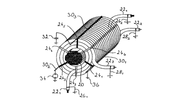
Figure 2 shows a perspective view of windings with one
earthing point per winding turn. Figure 2 shows a core leg
designated by the numeral 20 within a power transformer or
inductor. Two windings 221 and 222 are arranged around the
core leg 20 which are formed from the high-voltage cable
(10) shown in figure 1. With the aim of fixing windings 22,
and 222 there are, in this case, four radially arranged
spacer members 241, 242, 243, 24q per winding turn. As shown
in figure 2 the outer semi conducting layer is earthed at
both ends 261, 262, 281, 282 of each winding 221, 222. Spacer
member 241, which is emphasised in black, is utilized to
achieve one earthing point per winding turn. The spacer mem-
ber 241 is directly connected to one earthing element 301,
i.e, in the form of an earthing track 301, which is con-
nected 32 to the common earth potential at the periphery of
the winding 222 and along the axial length of the winding
222. As shown in Figure 2 the earthing points rest (one
point per winding turn) on a generatrix to a winding.
Figure 3 shows a perspective view of windings with two
earthing points per winding turn according to a first em-
bodiment of the present invention. In Figures 2 and 3 the
same parts are designated by the same numerals in order to
make the Figures more clear. Also in this case the two wind-
ings 221 and 222, formed from the high-voltage cable 10 shown
in Figure l, are arranged around the core leg 20. Spacer
CA 02276399 1999-06-29
WO 98/34245 PCT/SE98/00153
12
members 241, 242, 243, 249 are also in this case radially ar-
ranged with the aim of fixing the windings 221 and 222. At
both ends 261, 262, 281, 282 of each winding 221 and 222 the
second semiconducting layer (compare with Figure 1) is
earthed in accordance with Figure 2. Spacer members 241, 243
which are marked in black, are used in order to achieve
two earthing points per winding turn. Spacer member 241 is
directly connected to a first earthing element 301 and
spacer member 243 is directly connected to a second earthing
element 302 at the periphery of the winding 222 and along the
axial length of the winding 222. Earthing elements 301 and
302 may be in the form of earthing tracks 301 and 302 which
are connected to the common earth potential 32. Both earth-
ing elements 30~, 302 are coupled by means of an electric
connection 341 (cable). The electric connection 341 is drawn
into one slot 361 arranged in the core leg 20. The slot 361
is arranged such that the cross-section area A1 of the core
Ieg 20 (and thereby the magnetic flow cb) is divided into two
partial areas A1, A2. Accordingly, the slot 361 divides the
core leg 20 into two parts, 201, 202. This entails that cur-
rents are not magnetically induced in connection with earth-
ing tracks. By earthing in the above-mentioned way the
losses in the second semiconducting layer are kept to a
minimum.
Figure 4 shows a perspective view of windings with three
earthing points per winding turn according to a second em-
bodiment of the present invention. In Figures 2-4 the same
parts are designated by the same numerals in order to make
the Figures more clear. Also here two windings 221 and 222,
formed from the high-voltage cable 10 shown in Figure 1, are
arranged around the core leg 20. Spacer members 241, 242,
243, 24q, 245, 246, are also radially arranged with the aim
of fixing windings 221 and 222 . As shown in Figure 4 there
... ~_. ~ _t._~.. i
CA 02276399 1999-06-29
WO 98/34245 PCT/SE98/00153
13
are 6 spacer members per winding turn. At both ends 261, 262;
281, 28z of each winding 221, 22z the outer semi conducting
layer (compare with Figure 1) is earthed as in accordance
with Figures 2 and 3. Spacer members 241, 243, 245 which are
marked in black are used to achieve three earthing points
per winding turn. These spacer members 241, 243, 245 are ac-
cordingly connected to the second semiconducting layer of
the high power cable 10. Spacer member 241is directly con-
nected to a first earthing element 301 and spacer member 243
is directly connected to a second earthing element 302 and
spacer member 245 is directly connected to a third earthing
element 303 at the periphery of the winding 22zand along the
axial length of the winding 222. Earthing elements 301, 302,
303, may be in the form of earthing tracks 301, 302, 303 which
are connected to the common earth potential 32. All three
earthing elements 301, 302, 303 are joined by means of two
electric connections 341, 342 (cables). The electric connec-
tion 341 is drawn into a first slot 361 arranged in the core
leg 20 and is connected to earthing elements 30z and 303. The
electric connection 392 is drawn into second slot 362 ar-
ranged in the core leg 20. Slots 361, 362 are arranged such
that the cross-section area A, of the core leg 20 (and
thereby the magnetic flow cp) are divided into three partial
areas A1, A2, A3. Accordingly slots 361, 362 divide the core
leg 20 into three parts 201, 20z, 203. This entails that cur-
rents are not magnetically induced in connection with
earthing tracks. By earthing in the above-mentioned way
losses in the second semiconducting layer are kept to a
minimum.
Figures 5a and 5b respectively, show a perspective view re-
spectively a sectional view of a winding on an outer leg of
a three phase transformer with three legs with three earth-
ing points per winding turn according to a third embodiment
CA 02276399 1999-06-29
WO 98/34245 PCT/SE98/00153
14
of the present invention. In Figures 2 - 5 the same parts
are designated the same numerals in order to make the Fig-
ures more clear. A winding 221, formed from the high-voltage
cable 10 shown in Figure 1, is arranged around the outer leg
20 of the transformer. Additionally in this case spacer mem-
bers 241, 242, 243, 244, 245, 256 are arranged radially with
the aim of fixing the winding 221. At both ends of the wind-
ing 22z the second semiconducting layer(compare with Figure
1) is earthed (not shown in Figures 5a and 5b respectively).
Spacer members 241, 243, 295, which are marked in black, are
used to achieve three earthing points per winding turn.
Spacer member 241 is directly connected to a first earthing
element 301, spacer member 243 is directly connected to a
second earthing element (not shown) and spacer member 245 is
directly connected to a third earthing element 303 at the
periphery of the winding 221 and along the axial length of
the winding 221, Earthing elements 301 - 303 rnay be in the
form of earthing tracks which are connected to the common
earth potential (not shown). The three earthing elements 301
- 303 are joined by means of two electric connections 341,
342 (cables). The two electric connections 341, 342 are
drawn in two slots 361, 362, arranged in a yoke 38 connect-
ing the three earthing elements 301 - 303 to each other. The
two slots 361, 362 are arranged such that the cross-section
area A of the yoke 38, (and thereby the magnetic flux ~) is
divided into three partial areas A1, A2, A3. The electric
connections 391, 342 are threaded through the two slots 361,
36~ and over the front and back side of the yoke 38. By
earthing in the above-mentioned way the losses are kept to a
minimum.
Figure 6a and 6b respectively, show a perspective view re-
spectively a sectional view of a winding, on a central leg
of a three phase transformer with three or more legs, with
_.._._.-~..~..~~.._._.....~_~_.__
CA 02276399 1999-06-29
WO 98/34245 PCT/SE98/00153
three earthing points per winding turn according to a fourth
embodiment of the present invention. In Figures 2 - 6 the
same parts are designated the same numerals in order to make
the Figures more clear. A winding 22~, formed from the high-
5 voltage cable 10 shown in Figure 1 is arranged around the
central leg 20 of the transformer. Additionally in this case
spacer members 241 - 246 are arranged radially, three of
which 241, 243, 245 are used to achieve three earthing points
per winding turn. The spacer members 241, 24;, 245 are di-
10 rectly connected to the earthing elements 301 - 303, of which
only two are shown, in the same way as described above in
connection with Figures 5a, and 5b. The three earthing ele-
ments 301 - 303 are connected by means of two electric con-
nections 341, 342 (cables). The two electric connections 341,
15 342 are drawn into two slots 361, 362 arranged in a yoke 38.
The two slots 361, 362 are arranged such that the cross-
section area A of the yoke 38 (and thereby the magnetic flux
is divided into three partial areas A1, A2, A3. The two
electric connections 341, 34z are threaded through slots 361,
362 on both sides of the central leg 20 relative to the yoke
38. By earthing in the above-mentioned way the losses in the
second semiconducting layer are kept to a minimum.
The principles used above may be used for several earthing
points per winding turn. The magnetic flux, ~, is located in
the core with a cross-section area A. This cross-section
area A can be divided into a number of partial areas A1, Az,
... , An so that;
n
A=~A;
The circumference of a winding turn with length 1 can be di-
vided into a number of parts 11, 12, ... , In so that;
CA 02276399 1999-06-29
WO 98!34245 PCT/SE98/00153
16
n
No extra losses due to earthing are introduced if the elec-
tric connections are made in such a way that the ends of
every part li are electrically connected so that only the
partial area Ai is encompassed by a coil consisting of an
electric connection 66i and the segment li and the condition,
_~, _ _l;
1
is fulfilled, whereby ~ is the magnetic flux in the core and
~i is the magnetic flux through the partial area Ai.
If the magnetic flux density is constant throughout the en-
tire cross-section of the core, then ~ - B*A leads to the
ratio:
_A, _ _l;
A l
The power transformer/inductor in the above shown figures
comprises an iron core consisting of a core leg and a yoke.
It should however be understood that a power transformer/
inductor may also be designed without an iron core (air-
cored transformer).
The invention is not limited to the shown embodiments since
several variations are possible within the frame of the at-
tached patent claims.
.__.~_.._. T _.