Note: Descriptions are shown in the official language in which they were submitted.
.' ' CA 02276408 1999-06-24
15XZ04550
Method And Apparatus For Processing Partial Lines Of Scanned Images
Technical Field
This invention relates to the processing of sequences, particularly
partial lines of an image, such as X-ray images, and, more particularly, to a
technique for converting half lines of image pixel data to full-lines for
subsequent processing and display.
Background Art
Images generated by X-ray and other imaging systems are acquired
iri a variety of manners, depending upon the structure and configuration of
the detecting subsystems. In general, a detector is employed for receiving
image information divided into a matrix of pixels, which, together, deFne an
overall image of interest. The matrix of pixels is commonly ~ divided into
rows which are scanned and analyzed sequentially or in a pre-established
sequential pattern. The rows of pixels are then reassembled by processing
circuitry to reconstitute the useful image, which may be displayed or printed
for use by an attending physician or technician.
Various scanning formats and matrix sizes are commonly employed
in X-ray and other image processing modalities. In a number of these
techniques, the overall image is not only divided into rows of pixels, but
each row is further subdivided into half lines of pixels. For efficient
. 25 processing of the image data, the half lines of pixels may be detected
and
processed in various orders. For example, in a given matrix of image pixels,
half lines of pixel data may be acquired and processed beginning at upper
and lower outer edges of the image and proceeding toward a center line of
the image parallel to the half lines of pixels. In other processing
techniques,
half lines of pixel data may be processed from a center line of the overall
1
CA 02276408 1999-06-24
15XZ04550
image matrix, proceeding towards upper and lower edges. Moreover, half
lines of pixel data may also be acquired and processed progressively in
sequential half lines beginning at an upper comer of the image and
continuing to an opposite lower comer.
Depending upon the pixel data acquisition sequence utilized, pixel
data processed by the imaging system may arrive to signal processing
circuitry in interlaced half lines of data which must be sorted to produce a
meaningful image. In particular, where alternating half lines of data arrive
from opposite upper and lower portions of an image, the half lines of data
must be sorted and grouped into adjacent full-lines proceeding from one side
o~ the image to the other. In addition, the full-lines are arranged from an
upper or lower edge of the image to the opposite edge to reproduce the
arrangement of the pixels representative of the body or object scanned.
In addition to the sorting and reassociation functions performed on
interlaced half lines of image data, it is sometimes desirable to produce
scanned image data having different matrix dimensions (i.e., rows .of pixels
by columns of pixels), depending upon the type of feature being imaged and
the detail desired. Accordingly, circuitry employed for processing and
sorting half lines of pixel data would advantageously accommodate the
variety of matrix formats envisioned.
Disclosure of the Invention
In an exemplary embodiment, the invention provides an approach to
sorting partial or half lines of image data produced by an imaging detector.
The half lines of data are received by processing circuitry and are assigned
memory storage addresses. The memory storage addresses for each half line
of data are determined by a half line counter with reference to a base address
table. Values corresponding to output locations are stored in the base
2
CA 02276408 1999-06-24
15XZ04550
address table. The values are changed by reference to offsets. As the half
line counter is incremented for sequentially received half lines of data, the
memory addresses in which the data are stored are determined uniquely, by
reference to the base address table and offsets. The resulting sequence of
storage addresses orders the half lines of data to associate the data into
sequential full-lines for reconstitution of the scanned image.
The technique facilitates the use of various scan modes and matrix
sizes. By altering the base addresses and offsets used to generate the output
memory address locations, various scatuling modes may be employed,
including outside-to-inside scanning and inside-to-outside scanning.
lV~oreover, by setting the proper values in the base address table and by
using
appropriate offsets, a variety of pixel matrix dimensions may be
accommodated by the same system, in a computationally efficient manner.
Brief Description of the Drawings
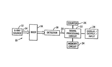
Fig. 1 is a diagrammatical representation of an X-ray imaging
system including circuitry for acquiring and processing half lines'of image
data;
Fig. 2 is a diagrammatical representation of an X-ray image divided
into half lines of pixel data in accordance with an outside-to-inside scan
mode;
Fig. 3 is a diagrammatical representation of a re-ordered sequence
of half line data for the image of Fig. 2, properly sorted to reconstitute the
image;
Fig. 4 is a base address table for assigning base addresses to half
lines of image data for the image illustrated in Fig. 2;
Fig. 5 is an offset table for applying relevant offsets to the base
addresses of the table of Fig. 4;
3
CA 02276408 1999-06-24
15XZ04550
Fig. 6 is an output memory address location table generated by
reference to the base address table of Fig. 4 and the offset table of Fig. 5
for re-ordering the half lines of image data from the scanned order of Fig.
2 to the order represented in Fig. 3; and
Fig. 7 is a flow chart illustrating exemplary control logic for
reordering partial-lines of image pixel data for subsequent storage and
processing.
Best Mode for Carrying Out the Invention
Referring now to Fig. 1, the primary components of an imaging
system 10 are illustrated as including an X-ray source 12 which is configured
to emit a stream 14 of X-rays upon demand. The X-rays are directed to a
body or subject 16. A portion of the X-rays pass through the body and
impact a detector 18. Detector 18 is configured to 'isolate discrete picture
elements or pixels and to generate signals representative of the intensity of
the radiation impacting the detector within each pixel. These signals are
transmitted from detector 18 as a data stream, represented by reference
numeral 20, to a signal processing circuit 22.
Signal processing circuit 22 conditions the data received from
detector 18, and refines the data to produce ordered data which can be
interpreted by an attending physician or technician. Signal processing circuit
22 is coupled to a memory circuit 24 which, for the present purposes, serves
to store partial lines of data for reconstitution of the image. Signal
processing circuit 22 is also coupled to a counter 26 which aids in reordering
data received from detector 18 as summarized below. A display/output/input
station 28, typically including a monitor or printer and an input station,
such
as a keyboard, is coupled to signal processing circuit 22 for producing a
reconstituted image which is available for interpretation by the attending
physician or technician. The physician or technician may also input
4
CA 02276408 1999-06-24
15XZ04550
operational parameters into circuit 22 via station 28, such as the image
matrix size and scanning pattern as discussed below. In general, such
parameters may be input by selection of an image or application type or of a
general examination configuration. It should be noted that signal processing
circuit 22 and counter 26 may be defined as appropriate code in a general
- purpose or application-specific microprocessor or computer. Moreover,
signal processing circuit 22 may perform functions in system 10 in addition
to those described below, such as image processing, analysis and
enhancement functions.
Fig. 2 illustrates an image generated by system 10 in the form of an
image pixel matrix 30. Matrix 30 includes a series' of discrete pixels
arranged in parallel rows 32 and parallel columns 34. The rows and columns
of pixels form an overall image having a width 36 and a height 38. The
particular dimensions of matrix 30 may be varied depending upon the type
of tissue or subject being scanned, and the types of features of interest
within
the image. For example, matrix 30 may have dimensions of 2,048 pixels by
2,048 pixels as a standard format, or may have a smaller format 1,024 pixels
by 1,024 pixels, such as for cardiac radiographs, or still different
dimensions,
such as 1920 pixels by 2304 pixels for mammograms.
In addition to accommodating various matrix or image sizes, system
10 may be configured to scan pixel data collected by detector 18 in various
modes. In particular, the modes may subdivide matrix 30 into regions
defined by a vertical center line 40 and a horizontal center line 42. Within
' these regions, scanning may progress in accordance with the predefined
modes. For example, in the embodiment illustrated in Figure 2, scanning
begins at a left edge 44, adjacent to an upper edge 46. Scanning then
progresses from left edge 44 in the direction of a right edge 48. Subsequent
data is scanned beginning from left edge 44, adjacent to a lower edge 50,
5
CA 02276408 1999-06-24
' 15XZ04550
proceeding from left edge 44 in the direction of right edge 48. The
information scalilled within the regions defined by the edges and the center
lines form half lines of pixel data, designated by reference numeral 52 in
Fig. 2. Each half line of pixel data includes signals or values representative
of the intensities within adjacent pixels in a row across matrix 30.
In one scanning mode illustrated in Fig. 2, which may be referred to
as an outside-to-inside scanning mode, a first half line of pixel data,
designated "1" is scanned in an upper left position in matrix 30. The
subsequent half line of pixel data, designated "2" extends along a lower left
comer of matrix 30. Due to the configuration of detector 18, the subsequent
half line "3" of pixel data extends from center line 40, adjacent to upper
edge 4G, toward right edge 48. Next, a half line "4" of pixel data is scanned
from center line 40 adjacent to lower edge 50, in the direction of right edge
48. In this mode, scanning proceeds in accordance with the foregoing order
until the rows of matrix 30 adjacent to horizontal center line 42 have been
scanned.
It should be noted that the information received from detector 18 by
signal processing circuit 22 may not only include interlaced half or partial-
lines of pixel data, but may include data in which pixels of partial lines are
further interlaced. However, the technique described below proceeds based
upon partial-lines in which individual pixels have been pre-sorted to fon~n
contiguous sequences or series of pixel data defining half lines, or more
generally, partial-lines. Moreover, it should be noted that the technique
described herein is not limited to the particular scanning sequence
illustrated
in Fig. 2. Rather, the technique may be applied to partial-lines of pixel data
scanned in both symmetrical and asymmetrical patterns, and in outside-to-
inside sequences, inside-to-outside sequences, or in progressive scanning
sequences. The particular scanning mode or sequence, and the particular
6
CA 02276408 1999-06-24
15XZ04550
matrix size may be configured as parameters recognizable by signal
processing circuit 22 which may be input by an operator or technician via
display/output/input station 28 (such as by selection of an image or
examination type as mentioned above).
Referring again to Fig. 2, depending upon the scanning sequence
selected, it will be apparent that the partial-lines of pixel data received by
signal processing circuit 22 will not correspond to the proper ordering of the
data in a reconstituted image matrix 30. To permit the data to be reordered
for presentation in a reconstituted image, signal processing circuit 22, in
conjunction with memory circuit 24 and counter 26, organizes the partial-
l~nes of data in an appropriate sequence as illustrated in Fig. 3. This
reordered sequence 54 may be conveniently configured in memory circuit 24
by assigning unique addresses 56 to the individual partial-lines of data. The
l5 sequence 54 illustrated ~in Fig. 3 corresponds to the appropriately ordered
half lines of pixel data illustrated in the scanning sequence of Fig. 2. The
reordered sequence thus penmits contiguous full lines of pixel data to be
defined for subsequent processing and display.
Figs. 4, 5, and 6 illustrate an exemplary technique employed by
signal processing circuit 22 for reordering the half lines of pixel data of
Fig.
2 into the desired sequence 54 of Fig. 3. In particular, Fig. 4 represents a
base address table 58 stored within memory circuit 24. Base address table
58 includes data associating specific element numbers 60 to base addresses
62. Fig. 5 represents an offset table 64, also stored within memory circuit
' 24, and associating element numbers 66 with offset values 68. Fig. 6
represents a half line storage address table 70, generated by reference to
base
address table 58 and offset table 64 as described below.
7
CA 02276408 1999-06-24
15XZ04550
To determine the half line storage addresses 74 of table 70, signal
processing circuit 22 executes control logic designed to assign unique
addresses to each partial-line of image data. This logic may proceed by
combining the base storage addresses of table 58 with offsets of table 64.
Exemplary steps in such control logic are illustrated in Fig. 7. As shown in
Fig. 7, the control logic begins at step 76 and proceeds to step 78 where the
first half line storage address is assigned to the first element by setting
the
half line storage address equal to the corresponding base address of table 58.
Hence,. the first half line storage address receives a value of BASE 0.
Thereafter, circuit 2~ proceeds to step 80 where the assigned value
&,om the base address table 58 is altered by combining the original base
address with an offset of table 64. In the illustrated embodiment,
programming code may be provided to reassign each base address value G2 a
new value corresponding to the previous value plus the offset for the
corresponding element found in table 64. Thus, following step 80, in the
illustrated embodiment, as elements 0-3 of table 58 are assigned to data,
these will be sequentially altered to contain values of BASE_0 +
OFFSET 0, BASE 1 - OFFSET 1, BASE 2 + OFFSET 2, and BASE_3
OFFSET 3, respectively.
Following step 80, counter 26 is incremented as illustrated at step 82.
At step 84 signal processing circuit 22 determines whether the counter value
has reached a predetermined modules value. In the illustrated example, a
modules value of 4 is used due to the four quadrants defined by center lines
40 and 42 in matrix 30 (see Fig. 2). So long as the counter value has not
reached the modules value, circuit 22 returns to step 78 to assign the next
base address value from table 58 to the subsequent half line of pixel data.
8
CA 02276408 1999-06-24
15XZ04550
Once the modulus value is attained by the counter 2G, circuit 22
proceeds to step 86 where it is determined whether the entire matrix has been
converted. This step may be performed by reference to half line counter
values as denoted by reference numeral 72 in Fig. 6. The total number of
half line counter values will correspond to the number of partial lines within
the image matrix 30, in turn dependent upon the dimensions 36 and 38 of the
matrix (see Fig. 2) and the selected scanning mode or sequence.
When the response at step 8ti is negative, circuit 22 proceeds to step
88 where counter 2G is reset. Thereafter, circuit 22 returns to step 78 to
assign the next group of half line pixel data the altered addresses then
stored
irl table 58. This control logic proceeds until the entire matrix 30 has been
converted, and is thereafter exited, as noted at step 90.
Although half line storage addresses 74 may be associated with the
pixel data to provide for reordering of the data, each set of pixel data is
preferably stored in the memory circuit 24 in an address location
corresponding to that dictated by table 70. It should also be noted that,
while
the foregoing technique reference has been made to tabulated data, those
skilled in the art will readily appreciate that the addresses, offsets and
resulting storage addresses could either be embodied in look-up tables as
described, or could be embedded in appropriate code executed by signal
processing circuit 22.
Those skilled in the art will also recognize that by altering the base
address and offset values utilized in determining the half line storage
addresses, the present technique can easily be adapted to accommodate
various image matrix dimensions, as well as various scanning modes,
including both inside-to-outside sequences and outside-to-inside sequences.
Moreover, the technique provides a particularly computationally efficient
9
CA 02276408 1999-06-24
~5XZ04550
system wherein contiguous full lines of pixel data can be obtained in real-
time as the half lines of data are transmitted to the signal processing
circuitry. The system is easily reconfigurable by inputting specific matrix
size selections and scanning mode selections via display/output/input station
28.