Note: Descriptions are shown in the official language in which they were submitted.
CA 02276726 1999-07-OS
WO 99/25159 , PCT/IB98/01743
Parallel-storage series-drive electronic ballast.
The invention relates to ballasts for lamps and, in particular, to electronic
ballasts for discharge lamps.
It has been estimated that over 25% of all electrical energy consumed in the
world is utilized
to power artificial lighting. Thus, the importance of efficient electrical
lighting sources cannot
be understated.
The most efficient electrical lighting sources, that are commonly ,available,
are
gaseous low-pressure and high-pressure discharge lamps, e.g. fluorescent and
high-intensity-
discharge (HID) lamps, respectively. These types of lamps typically have a
negative-
resistance characteristic and are driven by current-limiting circuits known as
ballasts.
Two general types of lamp ballasts, i.e. electromagnetic and electronic, are
in
common usage for driving discharge lamps. Electromagnetic ballasts have only
passive circuit
components and typically drive lamps at power-line frequencies. Electronic
ballasts include
both passive and active circuit components and typically drive lamps at
frequencies much
higher than power line frequencies. Generally, the electromagnetic ballast is
less expensive.
However, the electronic ballast is smaller and lighter, operates discharge
lamps more
efficiently) with less audible noise and with no visible flicker, and
contributes to a longer lamp
life. Additionally, electronic ballasts can regulate discharge-lamp power more
effectively than
electromagnetic ballasts in response to changing power-line and lamp-operating
conditions.
Figure 1 schematically illustrates a typical electronic ballast for driving a
discharge lamp L from an AC voltage vas provided by a power source PS, such as
power lines
from a local utility. The ballast includes an electromagnetic interference
filter EMI, a full-
wave rectifier bridge BR, a power-factor correction circuit, an energy-storage
capacitor C~,
and a half bridge resonant inverter, all electrically connected in series
between the power
source and the lamp L.
The filter EMI prevents electromagnetic interference generated by the ballast
circuitry and the discharge lamp from being conducted back to the power
source. The ballast
generates EMI in the form of high harmonic currents which, if conducted back
to the power
source, could cause problems such as excessive neutral currents, overheated
transformers, and
interference with any sensitive electronic equipment which also receives
electrical energy
CA 02276726 1999-07-OS
WO 99/25159 PCT/IB98/01743
2
from the power source. Discharge lamps can generate both electromagnetic and
radio-
frequency interference.
The power-factor correction circuit is a well-known boost-converter type,
including an inductor Lea, a switching transistor Q,o and a diode D,o. It
functions to increase
the power factor at the AC power source and to boost the DC voltage provided
to the energy-
storage capacitor C~ by the bridge BR.
The energy-storage capacitor C~ performs two functions. First, it acts as a DC
voltage source for the resonant inverter. Second, it balances the energy flow
between the load
and the power source.
When the AC power source PS is instantaneously supplying less power than the
load is consuming, C~ must deliver energy to the load. Conversely, when the AC
power
source is instantaneously supplying more power than the load is consuming, C~
must store
energy.
The resonant inverter output stage converts the DC voltage on the energy
storage capacitor Cr to a high frequency sinusoidal drive for the lamp L. Two
transistor
switches Q> > and Q,z are electrically connected in a half bridge
configuration and operate at a
50% duty cycle to chop the DC voltage into a high-frequency square wave. A
capacitor Cb is
provided for blocking DC components from reaching a transformer T, which is
provided for
both isolation and impedance matching. An inductor Lf and a capacitor Cf form
a second-
order filter for filtering the high-frequency square wave so that a sinusoidal
voltage and
current, at the fundamental switching frequency, are applied to the discharge
lamp L.
It is an object of the invention to provide an electronic ballast which
optimizes
the drive current for a discharge lamp to improve the radiation efficiency of
the lamp. For
maximum radiation efficiency, a constant DC drive current would be supplied.
This is not
practical, because a power-dissipating ballast resistor would be required.
Also, in fluorescent
lamps this would cause a unidirectional migration of ions in the discharge
column and the light
produced at one end of the lamp would be brighter than at the other. The
sinusoidal AC
current supplied by the prior art ballast of Figure 1 is a compromise. It
periodically reverses
the polarity of the drive current to achieve uniform brightness along the
length of the discharge
column) but the magnitude of the drive current is never constant.
It is another object of the invention to provide an electronic ballast which
is
compact and which does not contribute to electromagnetic interference
production by a .
CA 02276726 1999-07-OS
WO 99/25159 3 PCT/IB98/01743
discharge lamp. In the prior art ballast of Figure l, the size of the passive
filter components in
the resonant inverter can be reduced by increasing the operating frequency.
However,
increasing the operating frequency of the discharge lamp also increases
electromagnetic
interference energy radiated by the lamp.
It is yet another object of the invention to reduce the size of the energy
storage
capacitor required for a lamp ballast. The electronic ballast of Figure 1
supplies full-wave
rectified sinusoidal power to the capacitor C~ at twice the power source
frequency. At this
relatively low frequency, the power supplied to the capacitor is well below
peak amplitude for
relatively long intervals. In order to provide low-ripple power to the
resonant inverter) the
capacitor C~ must be physically large.
It is still another object of the invention to provide an electronic ballast
which
does not require the use of a transformer. The transformer utilized in an
electronic ballast such
as that shown in Figure 1 not only increases the size and weight of the
ballast, it also
contributes to electrical losses in the ballast.
It is a further object of the invention to provide an electronic ballast which
takes
advantage of improvements in semiconductor technology. The electronic ballasts
which are
commonly available to the lighting industry do not take full advantage of the
efficiencies in
size, power consumption and cost that are increasingly possible by utilizing
state-of the-art
integrated circuit technology, particularly in the power semiconductor field.
In accordance with the invention, an electronic ballast is provided for
converting an alternating voltage and current of predetermined wavefortn and
frequency)
supplied by a power source, to an alternating square-wave voltage and current
of said
frequency for supply to a discharge lamp. The ballast comprises at least one
capacitive
storage means, bridge switching means and high-frequency duty-cycle switching
means. The
bridge switching means and high-frequency duty-cycle switching means cooperate
to
periodically:
electrically connect the at least one capacitive storage means in parallel
with the
power source;
electrically connect the at least one capacitive storage means in series with
the
power source and the discharge lamp; and
regulate the average current provided to and from the at least one capacitive
storage means to effect production of said square-wave voltage and current.
The alternating square-wave DC drive voltage, and corresponding DC drive
current, produced by the ballast maximizes radiation efficiency of the
discharge lamp without
CA 02276726 1999-07-OS
WO 99/25159 4 PCT/IB98/01743
the need for a power-dissipating resistor while avoiding the unidirectional
ion migration that
would occur in fluorescent lamps if driven with a unidirectional DC current.
By utilizing duty-cycle switching at a very high periodic rate while producing
an alternating DC Lamp driving voltage at a low frequency, the ballast can be
made compact
without increasing electromagnetic interference energy radiated by the lamp.
By providing a switching arrangement for intermittently connecting a storage
capacitor in series with the power source and the discharge lamp, such that
the storage
capacitor combines with the power source in powering the lamp, rather than
independently
providing the full energy requirement of the lamp, the size of the storage
capacitor may be
much smaller than in prior art ballasts.
By producing the lamp drive power by utilizing the above described switching
and capacitive storage means, the need for a cumbersome and lossy transformer
is avoided.
Further, the switching means utilized in a ballast in accordance with the
invention are especially suitable for construction with power integrated
circuits.
Embodiments of the invention will be illustrated making use of a drawing. In
the drawing is
Figure 1 a schematic diagram of a prior art electronic ballast circuit.
Figure 2 is a schematic diagram of a discharge lamp system employing an
electronic ballast in accordance with the invention.
Figures 3a - 3d are waveform diagrams illustrating operation of the system of
Figure 2.
Figure 4 is a schematic diagram showing the electronic ballast of Figure 2 in
greater detail.
Figures Sa - Sf are waveform diagrams illustrating energy characteristics of
storage elements of the electronic ballast of Figure 2.
Figures 6a-6c are timing diagrams illustrating operation of bridge switches in
various embodiments of the invention.
Figure 7 is a schematic diagram showing a more-detailed embodiment of the
electronic ballast of Figure 4.
Figure 8 is a schematic diagram of a discharge lamp system incorporating
another embodiment of an electronic ballast in accordance with the invention.
CA 02276726 1999-07-05
WO 99/25159 5 PCT/IB98/01743
Figures 9a-9f are timing diagrams illustrating operation of high-frequency
switches in the embodiment of Figure 8.
Figure 10 is a schematic diagram of a discharge lamp system incorporating
another embodiment of an electronic ballast in accordance with the invention.
Figures 11 a-11 a are timing diagrams generally illustrating operation of the
embodiment of Figure 10.
Figures 12a-12f are timing diagrams illustrating operation of high-frequency
switches in the embodiment of Figure 10.
Figwe 13 is a schematic diagram of a discharge lamp system incorporating
another embodiment of an electronic ballast in accordance with the invention.
Figure 2 illustrates a discharge lamp system employing an electronic ballast
in
accordance with the invention. As shown, the ballast includes a shunt energy-
storage element
1 S 10, electrically connected in parallel with an AC power source PS, and a
series energy-storage
element 12, electrically connected in series with a discharge lamp L. The
power source
supplies sinusoidal voltage and current at a standard power utility frequency,
e.g. 60 Hz. Note
that the polarity symbols + and - indicate voltage polarities during positive
half cycles of the
power source voltage va~. The aaows indicate current directions as follows:
~ ie~ represents the AC power source current during positive half cycles;
i,st"P represents the lamp current during positive half cycles; and
lshunt and i$~rits represent the respective shunt and series storage element
currents
when electrical energy is being delivered to these elements.
Figures 3a - 3d generally illustrate operation of the ballast.
The shunt and series energy-storage elements, respectively, function to
capacitively charge
and discharge such that a sinusoidal source voltage v,~ and current i,~,.
supplied by the power
source PS, is converted to a square-wave current i~a",P and voltage vi$",~)
for driving the
discharge lamp L in synchronism with the source voltage and current. Thus,
during each hal f
cycle the lamp current and voltage remain at a constant DC value. Driving the
discharge lamp
with square-wave power yields a radiation efficiency which is equivalent to DC
operation,
which is significantly better than that obtainable with sinusoidal operation
at the power source
frequency.
CA 02276726 1999-07-OS
WO 99/25159 6 PCT/1B98/01743
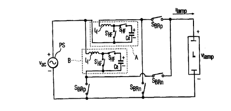
Figure 4 illustrates more completely the electronic ballast shown in Figure 2.
The ballast includes, in addition to the power source PS and the discharge
lamp L, two energy-
storage elements A and B, two bridge switches SBRp and two bridge switches
SBR". The bridge
switches function to alternately switch each of the elements A and B to the
shunt and series
electrical connections shown in Figure 2.
Specifically, during each positive half cycle of the AC source voltage vex,
the
two bridge switches SBRp are closed, thereby electrically connecting storage
element A in
parallel with the power source PS and storage element B in series with the
discharge lamp L.
Conversely, during each negative half cycle of the AC source voltage v~, the
two bridge
switches SBK" are closed, thereby electrically connecting storage element B in
parallel with the
power source PS and storage element A in series with the discharge lamp L.
Figures 2, 3a-3d, 4, Sa-Sf and 6a-6c collectively show how the shunt-connected
energy-storage element 10 operates to continually accumulate energy from the
power source
PS while the series-connected energy-storage element 12 continually delivers
energy to the
discharge lamp L.
During each positive half cycle Tp of the AC source voltage va~:
the voltage vsn"", across the shunt storage element 10 (momentarily storage
element A) is positive and has a magnitude equal to vas, the shunt current
lshunt is also positive,
except near the zero crossover of vsn""t, and net energy delivery to the shunt
storage element
(represented by the area under the power curve Psnunt) is positive; and
the voltage vs«~~$ across the series storage element 12 (momentarily storage
element B) is positive and adds to the positive-polarity source voltage vas to
produce the
positive half cycle DC lamp voltage v,""P, the series current i~~~s is
negative and has a
magnitude equal to that of the DC lamp current i,a,T,p, and net energy
delivery to the series
storage element (represented by the area under the power curve Ps~ries) is
negative.
During each negative half cycle T" of the AC source voltage v~:
the voltage vsn""t across the shunt storage element 10 (now momentarily
storage
element B) is negative and has a magnitude equal to v,~, the shunt current
isn"~, is also
negative, except near the zero crossover of vSn"~~, and net energy delivery to
the shunt storage
element (represented by the area under the power curve Psnunc) is positive;
and
the voltage vseri~ across the series storage element 12 (now momentarily
storage
element A) is negative and adds to the negative-polarity source voltage v8~ to
produce the
negative half cycle DC lamp voltage v~s",p) the series current is~;~s is
positive and has a
CA 02276726 1999-07-OS
WO 99/Z5159 ~ PCT/IB98/01743
magnitude equal to that of the DC lamp current i,a,m,, and net energy delivery
to the series
storage element (represented by the area under the power curve Ps~~~s) is
negative.
Note that, during the complete cycle encompassed by the time periods Tp and
T", the polarities of the voltages v~ and vB on the energy-storage elements A
and B,
respectively, never reverse. This simplifies construction of the storage
elements A and B.
Figure 7 shows the lamp system of Figure 4, but includes more-detailed
embodiments of the storage elements A and B. Each of these elements is
identical and
includes a charge-storage capacitor C~, two high-frequency duty-cycle switches
SHF and S'HF
and a filter inductor Lf. All switches in the ballast, including the bridge
switches SBRp and
SBR", are indicated schematically only and will be implemented in actual
circuitry by solid-
state semiconductor switches, such as power MOSFETs.
Each of the two capacitors Ce alternately charges from the power source PS and
discharges to the lamp L, while maintaining the polarity shown. The two high-
frequency
duty-cycle switches SHF and S'HF in each storage element operate alternately
during each of
successive periods THF which occur at a very high periodic rate (e.g. 100 kHz)
relative to the
periodic switching rate (e.g. 60 Hz) of the bridge switches Seap and SHR". The
f lter inductor
L~ in each storage element blocks high-frequency switching components from
reaching the
power source and the lamp.
With respect to each of the storage elements A and B:
~ When the bridge switches electrically connect the storage element in
parallel
with the power source) the closing of switch SHF in the respective element
places the
respective capacitor C~ in parallel with the power source (via the respective
filter elements Lf),
but the alternate closing of switch S'HF bypasses the capacitor. During each
period T,~F {e.g. 10
0 sec), switch SHF closes for the duration (DP)THF and switch S'HF closes for
the duration ( 1-
DP)THF, where Dp = Ov~O / v~~. Thus, the capacitor tends to be connected to
(and charged by)
the power source a large portion of periods THF when the instantaneous power
source voltage
vas has a large magnitude relative to the capacitor voltage v~~, but to be
bypassed a large
portion of periods THF when the instantaneous power source voltage vas has a
small magnitude
relative to the capacitor voltage.
~ When the bridge switches electrically connect the storage element in series
with
the discharge lamp, the closing of switch SHF in the respective element places
the respective
capacitor C~ in series with the lamp (via the respective filter inductors Lf),
but the alternate
closing of switch S' f,F bypasses the capacitor. Now, during each period THF
switch SHF closes
for the duration (DS)THF and switch S'HF closes for the duration (1-DS)THF,
where DS = Gv,amp -
CA 02276726 1999-07-OS
WO 99/25159 o PCT/IB98/01743
v,~~ / vie. Thus, the capacitor tends to be connected in series with the lamp
a large portion of
periods THF When the instantaneous power source voltage va~ has a lower
magnitude relative to
the desired lamp voltage, but to be bypassed a large portion of periods THF
when the
instantaneous power source voltage vas has a larger magnitude relative to the
desired lamp
voltage.
Note that the voltage drop across each of the filter inductors L,~ at the
relatively
low frequency of the voltages vA and vB is considered to be substantially
equal to zero. Note
further that, although no specific circuitry is described for duty-cycle
modulating the switches
SHF and S'HF in response to variations between the voltages vas) v,,mP and
vie, many suitable
circuits are well known in the art. See, for example, Principles of Power
Electronics by John
G. Kassakian, Martin F. Schlecht & George C. Verghese, pages 268-269, Addison-
Wesley
Publishing Company,1991.
Figure 8 shows a lamp system including an embodiment of an electronic ballast
in which only a single charge-storage capacitor is used to produce the voltage
and current
1S waveforms shown in Figures 3a-3d. As shown, the ballast includes a first
filter inductor Lf in
series with a power source PS, a second filter inductor Lf in series with a
discharge lamp L, the
charge-storage capacitor C~, two bridge switches SBRp, two bridge switches
SBR", and three
high-frequency duty-cycle switches SHFa SHF2 and SHF3. The four bridge
switches function to
alternate the polarity with which the capacitor C~ is connected in the ballast
during positive
and negative half cycles of the power source voltage v,~. The three high-
frequency switches
function to successively switch the capacitor C~ to each of three different
states of connection:
electrically connected in parallel with the power source PS (via the
respective
filter inductor Lf);
electrically connected in series with the lamp L (via the respective filter
inductor L~) and in the same polarity direction such that the voltages v,~ and
v~~ complement
each other;
operatively disconnected.
The two filter inductors Lf block high-frequency switching components from
reaching the
power source and the lamp. The filter inductor connected in series with the
lamp L also
ensures that the lamp voltage v~""P is affected by the duty-cycle or average
value of the storage
capacitor voltage vie in each of the above-listed states of connection where
the capacitor is
electrically connected to the lamp.
Operation of the bridge switches is in accordance with the timing shown in.
Figures 6a-6c. Specifically, during each positive half cycle of the AC source
voltage va~, the
CA 02276726 1999-07-OS
WO 99!25159 PCT/IB98l01743
9
two bridge switches SBRP are closed, thereby electrically connecting the
negative electrode of
the storage capacitor C~ to the terminal of the power source PS which is
momentarily negative.
Conversely, during each negative half cycle of the AC source voltage vas, the
two bridge
switches SBw, are closed, thereby electrically connecting the positive
electrode of the storage
capacitor to the terminal of the power source PS which is now momentarily
positive.
Operation of the three high-frequency duty-cycle switches is in accordance
with
the timing shown in Figures 9a-9f. Figures 9a-9c illustrate operation during
each positive
half cycle of the AC source voltage, while Figures 9d-9f illustrate operation
during each
negative half cycle. The periods TnF shown repeat at a very high periodic rate
(e.g. 100 kHz)
relative to the periodic switching rate (e.g. 60 Hz) of the bridge switches.
Each period THF is
divided into three successive sub-periods during which two of the three high-
frequency
switches always remain closed, to avoid interrupting current flow through the
lamp and the
power source. Specifically, in this exemplary embodiment:
switches SHF~ and SHFZ are closed during a respective sub-period T~z;
~ switches SHF~ and SHFS are closed during a respective sub-period T,3;
switches SHF2 and SHF3 are closed during a respective sub-period T23.
Referring to Figures 8 and 9a-9c together, it can be seen that during each
positive half cycle of
the source voltage va~, with the two bridge switches SgRp closed, the high-
frequency switch
pairs close in the sequence:
~ SHF1 ~d SHF3 clOSed simultaneously, thereby electrically connecting the
storage
capacitor C~ in series with the power source and the lamp;
~ SHF2 ~d SHF3 clOSed simultaneously) thereby electrically connecting the
storage
capacitor in parallel with the power source;
~ SHFI ~d SHF2 ~I~Sed simultaneously, thereby operatively disconnecting the
storage capacitor from the power source and the lamp.
Similarly, referring to Figures 8 and 9d-9f together, it can be seen that
during
each negative half cycle of the source voltage vex, with the two bridge
switches SgRn closed,
the high-frequency switch pairs close in the sequence:
SHFZ and SHF3 clOSed simultaneously, thereby electrically connecting the
storage
capacitor C~ in series with the power source and the lamp;
,SHF~ and SHF3 clOSed simultaneously, thereby electrically connecting the
storage
capacitor in parallel with the power source;
*rB
CA 02276726 1999-07-OS
WO 99/25159 1 O PCT/IB98/01743
~ SHFI ~d SHF2 clOSed simultaneously, thereby operatively disconnecting the
storage capacitor from the power source and the lamp.
The durations of the sub-periods depend on the state of connection of the
storage capacitor. Specifically:
When the capacitor is electrically connected in parallel with the power source
(during sub-period T23 in the positive half cycles and T13 in the negative
half cycles), the
duration of these sub-periods is (D~~uei)THF, where Dpanuei = wac 0 / v~. Thus
the capacitor
tends to be connected to (and charged by) the power source a large portion of
periods THF
when the instantaneous power-source voltage v,~ has a large magnitude relative
to the
capacitor voltage v~~.
When the capacitor is electrically connected in series with the discharge lamp
(during sub-period T, 3 in the positive half cycles and T23 in the negative
half cycles), the
duration of these sub-periods is (Ds~ries)THF~ where Ds~,.;~s = 0 vi,r"p - v,~
D / vie: Thus the
capacitor tends to be connected in series with the lamp a large portion of
periods THF when the
instantaneous power-source voltage vas has a lower magnitude relative to the
desired lamp
operating voltage v,amP.
When the capacitor is operatively disconnected (during sub-period T~z in both
the positive and negative half cycles), the duration of this sub-period is
(Dd;s~~nnect)THF~ where
Ddisconnect = v~~ - ~viame0 ~ v~~. The disconnected state enables independent
control of the
duty-cycle ratios Dpa~i,~, and D~~~g. NOte that Dp,~0e1 + Dseries +
Ddisconnoct ' 1.
One of the limitations of the ballasts of Figures 7 and 8 is that the power-
source
voltage must be lower than the lamp voltage, unless some modification is made.
Figure 10
illustrates one possible modification of the Figure 8 ballast which is capable
of producing a
lamp voltage that is not limited by the power source voltage. The ballast of
Figure 10 is
capable of both up-conversion and down-conversion of the power-source voltage
v,~. This
ballast is identical to that of Figure 8, except for the addition of:
a pair of up-conversion switches S~ for electrically connecting the storage
capacitor C~ and the high-frequency switches in an up-conversion mode during a
portion of
each half cycle of the power source voltage; and
~ a pair of down-conversion switches SD for electrically connecting the
storage
capacitor C~ and the high-frequency switches in a down-conversion mode during
a different
portion of each half cycle of the power source voltage.
CA 02276726 1999-07-OS
WO 99/25159 PCT/IB98/01743
11
Figures 11 a-11 a illustrate the operation, during a complete cycle of the
power
source voltage, of the up and down conversion switches S~ and So and of the
positive and
negative bridge switches SBRp ~d Sg~,. Note that the up-conversion switches Su
close when
the AC source voltage v,~ is lower than the desired operating voltage of the
lamp Viemp~
Conversely, the down-conversion switches SD close when the AC source voltage
ve~ is higher
than the desired operating voltage of the lamp v,a",P.
Whenever the up-conversion switches are closed) the ballast configuration is
identical to that of Figure 8 and operation is also identical to that
described for the Figure 8
embodiment.
Whenever the down-conversion switches are closed, the ballast configuration
and operation changes with respect to the high-frequency duty-cycle switches
SHF,, SHF2 ~d
SHF3~ Now the three high-frequency switches function to successively switch
the capacitor C
to each of three different states of connection:
electrically connected in parallel with the lamp L (via the respective filter
inductor Lf);
electrically connected in series with the power source PS (via the respective
filter inductor Lf) but in the opposite polarity direction such that the
voltages v,~ and vie work
against each other to decrease (from vex) the voltage applied to the lamp;
operatively disconnected.
Operation of the three high-frequency duty-cycle switches is in accordance
with
the timing shown in Figures 12a-12f. Figures 12a-12c illustrate operation
during each positive
half cycle of the AC source voltage) while Figures 12d-12f illustrate
operation during each
negative half cycle.
Referring to Figures 10 and 12a-12c together, it can be seen that during each
positive half cycle of the source voltage vas, with the switches So and SBRP
closed, the high-
frequency switch pairs close in the sequence:
SHF2 ~d SHF3 ClOSed simultaneously, thereby electrically connecting the
storage ,
capacitor C~ in parallel with the lamp;
SHF, and SHF3 closed simultaneously, thereby electrically connecting the
storage
capacitor in series with the power source and the lamp, with the polarities of
vas and v~~
opposing each other;
SHF, and SHFi closed simultaneously, thereby operatively disconnecting the
storage capacitor from the power source and the lamp.
CA 02276726 1999-07-OS
WO 99/25159 PCT/IB98/01743
12
Similarly, referring to Figures 10 and 12d-12f together, it can be seen that
during each negative half cycle of the source voltage vas, with the switches
Sp and SBA) closed,
the high-frequency switch pairs close in the sequence:
SHFI ~d SHF3 ~lOSed simultaneously, thereby electrically connecting the
storage
capacitor C~ in parallel with the lamp;
SHF2 ~d SHF3 ~lOSed simultaneously, thereby electrically connecting the
storage
capacitor in series with the power source and the lamp, with the polarities of
vas and vie
opposing each other;
SHp~ and S~(F2 clOSed simultaneously, thereby operatively disconnecting the
storage capacitor from the power source and the lamp.
The durations of the sub-periods depend on the state of connection of the
storage capacitor. Specifically:
When the capacitor is electrically connected in parallel with the lamp (during
sub-period TZ3 in the positive half cycles and T~3 in the negative half
cycles), the duration of
these sub-periods is (DParanel)THF, where Dpe~net = Dv~ar~,~D / v~~. Thus the
capacitor tends to be
connected to (and charged by) the power source a large portion of periods THF
when the
instantaneous lamp voltage v,a",p has a large magnitude relative to the
capacitor voltage v~~.
When the capacitor is electrically connected in series opposition with the
power source (during
sub-period T~3 in the positive half cycles and T23 in the negative half
cycles)) the duration of
these sub-periods is (Ds~ri~s)THF, where Ds~~es = D va~ - vi,ma D / v~~. Thus
the capacitor tends to
be connected in series opposition with the power source a large portion of
periods TNF when
the instantaneous power-source voltage vs~ has a higher magnitude relative to
the desired lamp
voltage.
When the capacitor is operatively disconnected (during sub-period T,2 in both
the positive and negative half cycles), the duration of this sub-period is
(Dd;sconnect)THF~ where
Ddisconnect - (Vce - DvacD) / vce.
As in the embodiment of Figure 10, Dp"~na + DS~,;~s ~' Ddisconnect = 1.
Figure 13 shows a lamp system including another embodiment of an electronic
ballast in which only a single charge-storage capacitor is used to produce the
voltage and
current waveforms shown in Figures 3a-3d. As shown, the ballast includes a
first filter
inductor L~ in series with a power source PS, a second filter inductor L~ in
series with a
discharge lamp L, the charge-storage capacitor C~, a bridge switch SBRp, a
bridge switch SBRn,
a first pair of alternately-closed) high-frequency, duty-cycle switches SHFa
and S'HF~, and a
second pair of alternately-closed, high-frequency, duty-cycle switches SHE,
atld S'HFh- The two
CA 02276726 1999-07-OS
WO 99/25159 13 PCT/IB98/01743
bridge switches function to alternate the polarity with which the capacitor C~
is connected in
the ballast during positive and negative half cycles of the power source
voltage v,~. The two
pairs of high-frequency switches function to switch the storage capacitor Ce
to any of four
different possible states of connection, i.e. with switches SHFa and SHFb
closed, switches SHFa
S and S'H~ closed, switches S'HFa and SHE, closed, and switches S'HFe and
S'Hn, closed.
Operation of the bridge switches is in accordance with the timing shown in
Figures 6a-6c. Specifically; during each positive half cycle of the AC source
voltage vas, the
bridge switch SBA is closed, thereby electrically connecting the negative
electrode of the
storage capacitor C~ to the terminal of the power source PS which is
momentarily negative.
Conversely, during each negative half cycle of the AC source voltage v,~, the
bridge switch
SBR" is closed, thereby electrically connecting the positive electrode of the
storage capacitor to
the terminal of the power source PS which is now momentarily positive.
The two pairs of high-frequency duty-cycle switches operate independently of
each other. They all operate continually, during both the positive and the
negative half cycles
of the AC source voltage, at a very high periodic rate (e.g. 100 kHz) relative
to the periodic
switching rate (e.g. 60 Hz) of the bridge switches. However, at any instant in
time, only one
of the switches in each pair is closed.
Note that the ballast of Figure 13 may be operated either in an up-converter
(va~
0 v,~",p) mode or in a down-converter (ve~ 0 v,amP) mode. Both modes of
operation are
described:
Up-converter Mode
During each of the high-frequency periods THF (e.g. 10 D sec) that occurs when
v,~ is in a positive half cycle:
~ switch SHFa is closed for the duration (Dw)THF and switch S'HFa is closed
for the
remainder of the respective period, i.e. for the duration (1 - DPa)THF) where
Dp~ = Cva~G / v~r;
and
~ switch SHFb is closed for the duration (DPb)THF and switch S'HFb is closed
for the
remainder of the respective period) i.e. for the duration (1 - DPb)THF, where
Dpb = OV~amP~ /
v.
Similarly, during each of the high-frequency periods THF that occurs when va~
is
in a negative half cycle:
~ switch S'HF~ is closed for the duration (D~,)THF and switch SHF, is closed
for the
remainder of the respective period, i.e. for the duration (1 - D"~)THF, where
D"a = Ova~O /.v~~;
and
CA 02276726 1999-07-OS
WO 99/25159 14 PCT/IB98/01743
. switch S'H~ is closed for the duration (Dnb)THF and switch SHFn is closed
for the
remainder of the respective period, i.e. for the duration (1 - D"b)THF, where
Dnb = O ViBmp~ ~
Vce.
Three important states of connection of the storage capacitor C~ exist:
a parallel state, when the capacitor is electrically connected in parallel
with the
power source PS (via respective filter inductor Lf);
. a series state, when the capacitor is electrically connected in series with
the
discharge lamp (via respective filter inductor Lf), and in the same polarity
direction, such that
the voltages va~ and v~~ complement each other;
~ operatively disconnected.
The parallel state occurs onlv when:
in positive half cycles SHFa is closed, i.e. for the duration (Dpe)THF, where
Dpa =
0 vac O / vc~; and
in negative half cycles S'HF8 is closed, i.e. for the duration (D"~)THF, where
D~e =
D vec 0 / vc~.
Thus the capacitor tends to be connected in parallel with (and charged by) the
power source during portions of both the positive and negative half cycles
when the
instantaneous power-source voltage v,~ has a large magnitude relative to the
capacitor voltage
v~~.
The series state occurs onlv when:
. in positive half cycles S'HFa ~d SH~n ~'e closed simultaneously, i.e. for
overlapping sub-periods having the durations (1-Dp,)THF (where Dp$ = Ova~O /
v~~) and
(Dpb)THF (where Dpb = OViamp~ I Vie); and
in negative half cycles SnFe and S'Hn, are closed simultaneously, i.e. for
overlapping sub-periods having the durations (1-D"a)TH~ (where D"e = Ov8~0 /
v~~) and
(Dnb)THF (where Dnb = 0 V~amp~ / Vce)
Thus the capacitor tends to be connected in series with the lamp and the power
source when
the magnitude of the instantaneous power source voltage tends to be small
relative to the
magnitude of the lamp voltage.
The disconnected state occurs g~jy when:
CA 02276726 1999-07-OS
WO 99/25159 15 PCT/IB98/01743
. in positive half cycles S'HFa ~d S~HFb ~'e closed simultaneously, i.e. for
overlapping sub-periods having the durations ( 1-Dpa)THF (where Dpa = D vas 0
/ vie) and ( 1-
Dpb)THF (where Dpb = ~V~""p0 / Vie); and
in negative half cycles SHF, and SHF~ are closed simultaneously, i.e. for
overlapping sub-p eriods having the durations ( 1-Dne)THF (where Dna = D va~ ~
/ vee) and ( 1-
Dnb)THF (where Dnb = ~V~ampO / Vce)~
Down-converter Mode
During each of the high-frequency periods THF (e.g. 10 sec) that occurs when
va~ is in a positive half cycle:
. SWItCh SHFa is closed for the duration (Dp,)THF and switch S'HFe is closed
for the
remainder of the respective period, i.e. for the duration (1 - Dpa)THF, where
Dpe = Ove~~ / v~~;
and
switch S'HFb is closed for the duration (Dpb)THF and switch S'IiFb is closed
for the
1 S remainder of the respective period, i.e. for the duration ( 1 - Dpb)THF,
where Dpb = O Vamp O /
Vce~
Similarly, during each of the high-frequency periods THF that occurs when vas
is
in a negative half cycle:
~ switch S'HFe is closed for the duration (Dn,)THF and switch SHFa is closed
for the
remainder of the respective period, i.e. for the duration (1 - Dna)THF, where
Dn~ = Ova 0 / v~e;
and
. switch S'HFb is closed for the duration (Dnb)THF and switch SHF,, is closed
for the
remainder of the respective period, i.e. for the duration (i - Dnb)THF, where
Dnb = ~Vlamp~) /
Vce~
Three important states of connection of the storage capacitor Ce exist:
a parallel state) when the capacitor is electrically connected in parallel
with the
Tamp (via respective filter inductor L~); and
. a series state, when the capacitor is electrically connected in series with
the
power source (via respective filter inductor L f)) but in the opposite
polarity direction, such that
the voltages v,e and vee work against each other to decrease (from v~~) the
voltage applied to
the lamp;
~ operatively disconnected.
The parallel state occurs only when:
CA 02276726 1999-07-OS
WO 99/25159 PCT/IB98/01743
16
in positive half cycles SHn, is closed, i.e. for the duration (DPb)THF, where
Dpb =
O v,a",~ 0 / v~~; and
in negative half cycles S'Hn, is closed, i.e. again for the duration (D"b)THF~
where D"b = D viamp 0 / Vce~
Thus the capacitor is connected in parallel with the lamp for sub-periods that
are proportional
to the lamp voltage.
The series state occurs g~,ly when:
in positive half cycles SH~a and S'Hn) are closed simultaneously, i.e. for
overlapping sub-periods having the durations (Dpa)THF (where DPa = way 0~ I
v~~) and ( 1-
lO Dpb)THF (where DPb = w,8",p0 / v~~); and
. in negative half cycles S'HFe and SHn, are closed simultaneously, i.e. for
overlapping sub-periods having the durations (D"a)THF (where D"a = 0 v,~ 0 /
v~~) and ( 1-
Dnb)THF (where D~b = Ova""P~ / v~~).
Thus the capacitor tends to be connected in series with the lamp and the power
source when
the magnitude of the instantaneous power source voltage tends to be large
relative to the
magnitude of the lamp voltage.
The disconnected state occurs fly when:
. in positive half cycles S'HFa and S'Hn, are closed simultaneously, i.e. for
overlapping sub-periods having the durations (1-DPa)THF (where Dpa = Ov8~0 /
vie) and (1-
2O Dpb)THF (where Dpb = Oviemp0 / v~~) ~d~
in negative half cycles SHFa and SHE are closed simultaneously, i.e. for
overlapping sub-periods having the durations (1-D"e)THF (where D"a = Ov8~0 /
v~e) and (1-
Dnb)THF (where Dr,b = CJV~amp~ I v~~).