Note: Descriptions are shown in the official language in which they were submitted.
CA 02276836 2007-02-08
1
MODULAR HIGH SPEED CONNECTOR
Background of the Invention
1. Field of the Invention:
This invention relates to electrical connectors. More specifically, but not
exclusively, the
present invention relates to high speed, modular cable connectors.
2. Brief Description of Prior Developments:
US Patent No. 5,924,899 granted on July 20, 1999 to the assignee of the
present
patent application discloses high speed cable connectors having terminal
carriers
mounted on circuit substrates. These connectors are modular and provide high
performance. However, there is a desire to maintain such performance but
reduce
manufacturing costs.
Summary of the Invention
According to the present invention, there is provided an electrical connector
comprising:
a) an insulative body having opposed first and second major surfaces and a
plurality of
edge members extending between the first and second major surfaces; b) an
access
opening in the insulative body to allow access to an end portion of a
flexible conductor with at least two wires into an interior portion of the
insulative body; c)
at least one electrically conductive terminal; and d) a circuit substrate
adapted to be
mounted on one of the first and second major surfaces, in overlying
relationship with
terminal receiving cavities and the access opening, the circuit substrate
having
electrically conductive traces extending between the terminal receiving
cavities and the
CA 02276836 2007-02-08
la
access opening. The electrical connector further comprises a plurality of
conductor
receiving cavities, one for each wire, adapted to receive the flexible
conductor and
formed in the insulative body at a location spaced apart from a mating
interface.
The present invention also relates to a method of making a connector
comprising: a)
providing a circuit substrate having at least one conductive trace; b)
providing an
insulating body having a plurality of terminal receiving cavities and a
plurality of conductor
receiving cavities; c) inserting and retaining a terminal in the terminal
receiving cavities;
d) mounting the circuit substrate on the body with a first portion of the
conductive trace
adjacent the terminal and a second portion of the trace adjacent the conductor
receiving
cavities; and e) establishing an electrical connection between the terminal
and the
conductive trace.
The foregoing and other objects, advantages and features of the present
invention will
become more apparent upon reading of the following non-restrictive description
of an
illustrative embodiment thereof, given by way of example only, with reference
to the
accompanying drawings.
Brief Description of the Drawings
In the appended drawings:
Figure 1 is an isometric view of a first embodiment of a cable connector in
accordance
with the invention;
Figure 2 is an exploded view of the connector shown in Figure 1;
CA 02276836 1999-07-05
2 6186
Figure 3 is a top view of the frame of the connector shown in Figures 1
and 2;
Figure 4 is a side cross-sectional view taken along line 4-4 of Figure 3;
Figure 5 is a plan view of the opposite side of the frame shown in Figure
3;
Figure 6 is an end view taken from the left-hand side of Figure 3;
Figure 7 is an isometric view of a contact terminal used in the
connector illustrated in Figure 1;
Figure 8 is a side elevational view, partially in cross-section, of the
terminal shown in Figure 7 mounted in a terminal cavity;
Figure 9 is an isometric view of the opposite side of the connector
shown in Figure 1;
Figure 10 is an isometric view of a partially assembled modular cable
connector using a plurality of modules of the type shown in Figure 1;
Figure 11 is an isometric view of a second embodiment of cable
connector frame;
Figure 12 is an exploded isometric view showing an assembly of
elements utilizing the frame of Figure 11;
Figure 13 is an isometric view showing the insertion of terminals into
the frame of Figure 11;
Figure 14 is an isometric view of the assembly shown in Figure 13 with
terminals retained in the frame;
Figure 15 is an isometric view of the opposite side of the frame shown
in Figure 11;
Figure 16 is an exploded isometric view of a third embodiment of the
invention;
CA 02276836 1999-07-05
~ =/
3 6186
Figure 17 is an isometric view of the assembly formed from the parts
shown in Figure 16;
Figure 18 is an exploded isometric view of the elements depicted in
Figure 16 and a shield plate;
Figure 19 is an isometric view of a terminal used in the embodiment
illustrated in Figures 16-18;
Figure 20 is a side elevational view of the terminal shown in Figure 19;
Figure 21 is a top plan view of the terminal illustrated in Figures 19
and 20; and
Figures 22 and 23 are cross-sectional views illustrating attachment of
wires to circuit substrates.
Detailed Description of the Preferred Embodiments
Several embodiments are explained in the following description.
Similar elements in each embodiment are identified by the same reference
numeral, differentiated between embodiments by the use of single or
multiple prime designations.
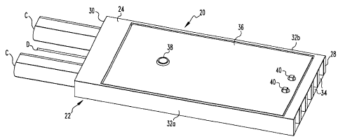
Figure 1 illustrates a cable connector module 20 embodying the
invention. The module 20 is formed of an insulative or dielectric body 22
that has a generally frame-like configuration defined by two opposed
major surfaces 24 and 26 (Figure 4) that are joined by a front edge
member 28, a back edge member 30 and a pair of side edge members 32a
a.nd 32b. The body 22 is preferably formed by molding a polymeric resin
having appropriate strength and heat resistant characteristics. The front
edge member 28 defines a mating interface for receiving terminals of a
mating connector through a plurality of openings 34. For example, the
module 20 could mate with one column of an array of terminal pins
arranged in rows and columns in a pin header backplane connector, with
CA 02276836 1999-07-05
4 6186
such pins generally be inserted into the openings 34 in a direction parallel
to the longitudinal axis of the module 20.
A circuit substrate 36, preferably a generally planar printed circuit
board, is received on one of the major sides 24 of the frame 22. The circuit
substrate 36 is retained and located with respect to the frame 22 by a
securing/locating post 38 receivable in opening 39 (Figure 2) and a pair of
locating lugs 40 received in openings 41. The post 38 and lugs 40 can also
function as stand-offs to achieve a desired terminal pitch distance
between adjacent stacked modules 20, as later explained. The outer
surface of the circuit substrate 36 is preferable coplanar with surrounding
portions of the frame 22. If shielding is desirable, the substrate 36 may be
of multi-layer construction, incorporating a ground plane.
Cables C, which may or may not be accompanied by an associated
drain wire D are introduced into the interior of the frame 22 through the
rear edge member 30. As shown, each of the cables C preferably
comprises a two wire, differential pair conductor. Such cables may
include shielding (not shown).
Referring to Figures 2-6, the frame 22 includes shoulder surfaces 42
along each of the side edge members 32a and 32b. The circuit substrate
36 rests on these shoulder surfaces as well as other surfaces within the
frame that are coplanar with shoulder 42.
' A plurality of terminal receiving cavities 44 are formed along the front
edge of the frame for receiving terminals 58 that are described below in
more detail. Each of the cavities 44 is aligned with one of the openings 34
along the front edge member 28. Each cavity includes a terminal retention
section such as a recess 46. The back ends of the cavity 44 are partially
closed off by pairs of wall members 47. As illustrated in Figure 2, the
CA 02276836 1999-07-05
6186
terminals 58 are inserted in the cavities 44 generally in the direction of
arrow F. That is, generally in a direction that is perpendicular to the plane
formed by the major surface 24.
A plurality of wire receiving cavities 48 are formed adjacent the rear
5 edge member 30 of the frame 22. Dividing walls 50 form two cavities 48,
one for each wire W of cables C. The cavities 48 communicate with cable
entry openings 52 formed through the end member 30. If a drain wire D is
present, the frame 22 will also include a drain wire cavity 54. The drain
wire D enters the cavity 54 through a drain wire slot 56 (Figure 5). When
the circuit substrate 36 is mounted on the frame 22, access to wires W
can be obtained from major surface 26 to secure the wires W onto the
circuit substrate 36, as by soldering, welding, conductive adhesives or
other means commonly used for obtaining electrical continuity between
wires W and appropriate contact pads of circuit substrate 36.
Figure 7 is an enlarged view showing a typical receptacle terminal 58.
The terminal preferable includes a generally U-shaped base/securing
section 60 having a generally flat base member 62 and two opposed arms
64a and 64b extending from each end of the base 62. Each arm 64a and
64b includes a distal mounting portion 66. Each distal mounting portion
is bounded by a rear edge 65 and a front edge 67. Preferably a retention
element, such as a barb 68, is carried on one or both of the edge surfaces
65 and 67. The bottom surface 70 of the base 62 is preferably flat and is
plated or prepared in a manner that is receptive to solder. A pair of
cantilever beams 72 extends from the base section 66 and carry opposed
contact surfaces 74 that are adapted to engage a mating pin. The terminal
58 is preferably formed as a one piece stamping of suitable electrical
CA 02276836 1999-07-05
--- ~.J
6 6186
terminal material, such as beryllium copper alloys and phosphor bronze
alloys.
Figure 8 illustrates the manner in which a terminal 58 is secured into
a terminal cavity 44. The back end of the cavity includes a pair of end
walls 47 and an intermediate retaining wall 49. The distance between the
front surface 47a of each wall 47 and the rear surface 49a of the retaining
wall 49 is substantially equal to the length, in the longitudinal direction of
cavity 44, of the distal portion 66 of each terminal arm so that the distal
portion 66 is received in an interference fit relationship in the slot 46
formed between front surface 47a and rear surface 49a. The retention
barbs 68 engage the surfaces 49a of the retaining walls 49 for additional
securing of the terminal 58 in the cavity 44.
The terminal 58 is retained in the frame 22 in a manner such that the
surface 70 of the terminal is either coplanar with or spaced slightly by a
distance t (Figure 8)from the support plane formed by the supporting
surfaces 25, such surfaces generally comprising the shoulder surface 42
and the top surfaces of the walls between cavities 44 and cavities 48.
Such positioning is desirable to accommodate the presence of an
adequate amount of solder paste disposed between the surfaces 70 and
the facing surface of the circuit substrate 36. A complete connected
module 20 is made by inserting a plurality of terminals 58 into terminal
cavities 44. A quantity of solder paste is applied to the circuit substrate
36 by conventional means, such as through a solder mask. Then, the
circuit substrate 36 is pressed onto the frame 22 and is held into position
by the peg 38 and lugs 40. Thereafter, the assembly comprising the frame
22, circuit substrate 36 and terminals 58 undergoes a re-flow operation to
effect a solder connection between the terminals 58 and contact pads (not
CA 02276836 1999-07-05
7 6186
shown) at the front ends of circuit traces T (Figure 9) of the circuit
substrate 36. Such an assembly can then be affixed to cables to form a
cable assembly by soldering the stripped portions R of wires W (Figure 1)
to contact pads (not shown) at the rear ends of tracks T.
Such a cable assembly is illustrated in Figure 9. As shown, each of the
conductors or wires W from one of the cables C is positioned in one of the
wire cavities 48 by inserting the cable end through an opening 52 in the
end member 30. Each of the wires W is arranged on one or the other side
of wall 50. The stripped ends of wires R are positioned over appropriate
contact pads formed at the ends of circuit traces T on the circuit
substrate 36. By reason of the fact that the cavities 48 are open to the
major surface 26, there is ready access to the wires W for purposes of
soldering, welding or otherwise securing such conductors to the circuit
traces T. If a drain wire D is present, in a similar fashion it is introduced
into an appropriate cavity 54 through grove 56. The cavity 54 provides
access for soldering or otherwise affixing the drain wire D to an
appropriate trace on the circuit substrate 36. The surface 26 of the frame
22 is provided with locating features, such as the circular boss 75 (Figure
9) and locating lugs 77. The boss 75 is sized and positioned to engage the
peg 38 of an adjacent stacked module and the locating lugs 77 are sized
and positioned to receive and locate the lugs 44 of an adjacent stacked
rriodule, thereby facilitating alignment of the modules 20. The module to
module terminal pitch distance, for example 2 mm to match the 2mm
centerline pitch between adjacent columns of a pin header, be regulated
by the axial length of post 38 and the height of lugs 40 andJor the height
of boss 75 and lugs 77. As a result, these elements may create a stand-off
CA 02276836 2007-02-08
8
distance or air gap between adjacent stacked modules, that can influence
impedance
of the connector.
Referring to Figure 10, a multi-conductor shielded cable connector can be
formed by
stacking a plurality of modules 20 and enclosing the stack within mating
halves 76 of a
shield. Mating shields of this type have previously been described in
published PCT
Patent Application WO 97/47058 filed in the name of the assignee of the
present patent
application.
In Figures 11, 12, 13 and 14, a second embodiment of connector module 20' is
illustrated. Referring to Figure 11, the frame or body member 22' has many of
the
features of the frame 22 previously described. It differs primarily in the
addition of
locating/guidance bodies 78a, 78b and 78c formed on side member 32a' and
locating/guidance members 78d, 78e and 78f formed on side member 32b' (Figure
12).
The members 78a-d primarily provide a means for locating the modules in
correct
orientation in a shield, such as shield 76, and provide guidance structures
extending
beyond the shield for guiding a cable connector into a mating header, as
described in
the patent applications identified in the previous paragraph.
The bodies 78a-78d are arranged so that the distance S (Figure 12) is just
slightly
greater than the width of module 20. Thus module 20 as shown in the previous
embodiment, can be located and aligned in stacked relation to a module 20'
formed
from the frame member 22'. Terminal
CA 02276836 1999-07-05
~
9 6186
pitch between modules can be controlled by the height of boss 75' and
standoffs 41' (Figure 12).
As illustrated in Figures 12 and 13, the terminals 58 are inserted into
terminal cavities 44' and are retained therein by structure as illustrated
in the previous embodiment. Once the assembly of the frame 22' and
terminals 58 is completed, that assembly is associated with a circuit
substrate 36. Under preferred manufacturing conditions, the individual
circuit substrates 36 are formed in multiples from a larger sheet
represented by the numera180. The individual substrates 36 are held in
the larger sheet by narrow bridging elements 82 that are designed to be
easily ruptured. Each of the substrates includes terminal contact pads 84
and wire contact pads 86 formed at each end of continuous circuit traces
(not shown). Substrate 86 also includes a ground contact pad 88 that
includes a generally width-wise extending portion 89. The ground pad 88
may have a ground wire, if present, soldered to it. Also, shields, if present
in the cables C, can be soldered or otherwise electrically associated with
the width-wise extending portion 89. The ground pad 88 may be
connected to a ground plane (not shown) formed within the circuit
substrate 36. A connector module is assembled in the manner previously
described, using a preferred technique of applying solder paste through a
mask to the terminal contact pads 84. The assembly comprising the frame
22' and terminals 58 is then pressed onto the circuit substrate and the
resulting assembly thereafter undergoes a reflow operation to solder the
terminals onto circuit substrate 36.
As in the previous embodiment, the frame 22' includes openings 52'
and 56' for the cables and drain wire, as previously described. As shown
in Figure 14, the terminals 58 are assembled in the frame 22' with the
CA 02276836 1999-07-05
~- ~
6186
solder receiving surfaces 70 of the terminals coplanar or slightly spaced
from the plane formed by the surfaces 25'.
Figures 16-18 illustrate a third embodiment of connector module 20".
This embodiment differs from the previous embodiments by elirninating
5 the need for the circuit substrate 36, 36'. In this embodiment, the frame
22" includes a plurality of terminal receiving cavities 44' that
communicate with pin receiving openings 34". The contact terminals 90
are inserted into the cavities 44" through the major surface 26" that is
opposite to the major surface 24 and 24' of the previous embodiments. As
10 in previous embodiments, the end member 30" includes cable receiving
openings 52' for receiving cables in cable receiving cavities 48" that are
formed on each side of separating walls 50". The cavities 44" differ from
those previously described by having a pair of flanking terminal securing
walls 91 formed in each cavity (Figure 17). The walls 91 each have a
forwardly disposed surface 92 and a rearwardly disposed surface 94. In
addition, the cavities 44" extend rearwardly and have a floor section 96
extending to the wire receiving cavities 48". Referring to Figures 19, 20
and 21, each terminal 90 includes a U-shaped base section having a
transverse base 62' and a pair of upstanding arms 64a' and 64b' as
previously described. Cantilever beams 72' extend forwardly from the
arms 64a', 64b' and carry contact sections 74' for engaging a pin. Each of
the terminals 90 includes a rearwardly extending neck portion 98 and a
securing plate 100 having laterally extending portions. The laterally
extending portions include locking tabs 102 that preferably are lanced
from plate 100. A terminal tail portion 104 extends from the plate 100.
The base 62, neck 98 plate 100 and tail portion 104 preferably are
substantially coplanar and colinear.
CA 02276836 1999-07-05
~- = ~
11 6186
As illustrated in Figure 17, the terminals 90 are pressed into the
cavities 44'. The terminals 90 are retained by an interference fit formed
between the surfaces 92 and 94 of the securing walls 91 and the rear edge
surfaces 65 and forward surfaces of the locking tabs 102. As shown in
Figure 17, the two pairs of outer terminals 90 are each positioned with
the securing base 100 and tail 104 resting on the floor 96 of the cavity.
Wires are inserted into the wire cavities 48" with insulation stripped
portions overlying the tail portions 104. Attachment of the wires to the tail
portions by soldering, welding, conductive adhesives or other means, such
as IDC connections, crimping etc. can readily be achieved through open
major side 26'.
In this embodiment, the centrally disposed termina190' is meant to
function as a ground terminal. In this case, the cavity 44" receiving the
terrnina190' has a shorter floor section 99 so that the tail portion 104
extends beyond the floor for purposes as will be later described.
Referring to Figure 18, this third embodiment can include a shield
plate 106 disposed on one side of the module. The shield plate 106
includes a pair of upstanding, preferably barbed retaining tangs 108. The
retaining tangs 108 are received in slots 112 (Figure 17) and retained
therein by an interference fit, thereby holding the shield onto the frame
22". As shown in Figure 18 the shield 106 also includes a raised contact
portion 110. When the shield is fixed onto the frame 22, the contact
member 110 engages the underside of the tail section 104 of the ground
terminal 90', thereby establishing an electrical connection between the
ground termina190' and shield. As with previous embodiments, provision
can also be made for ground wires and shielding braids to be attached to
the shield 106.
CA 02276836 1999-07-05
12 6186
As previously described and with reference to Figures 22 and 23, the
stripped portions R of wires W are affixed to contact pads 114 of the
traces by suitable means. One particular means that has been found
particularly useful is to pre-tin the strands of the wires w and then solder
them onto the pads 114 by means of an appropriately shaped tool 116,
that essentially comprises a heated electrode. Of course, other means may
be utilized for soldering, welding or otherwise electrically and
mechanically fixing the wires W onto the contact pads 114.
While the present invention has been described in connection with the
preferred embodiments of the various figures, it is to be understood that
other similar embodiments may be used or modifications and additions
may be made to the described embodiment for performing the same
function of the present invention without deviating therefrom. Therefore,
the present invention should not be limited to any single embodiment, but
rather construed in breadth and scope in accordance with the recitation
of the appended claims.