Note: Descriptions are shown in the official language in which they were submitted.
CA 02277181 1999-06-25
SPECIFICATION
Card Mounted with Circuit Chip and Circuit Chip Module
Technical Field
The present invention relates to a card mounted with a circuit chip,
and a circuit chip module. Particularly, the present invention relates to a
circuit chip mounted card and a circuit chip module realizing improvement
of reliability and reduction in fabrication cost.
Background Art
A non-contact type IC card is used in automatic examination for lifts
in skiing grounds and railroads, automatic sorting of parcels, and the like.
An example of a conventional non-contact IC card is shown in Fig. 7. An
IC card 2 shown in Fig. 7 is a one-coil type IC card, including a coil 4 used
as an antenna, capacitors C1 and C2, and an IC chip 8.
Capacitors C1 and C2 and IC chip 8 are mounted on a film-like
synthetic resin substrate. The substrate mounted with capacitors C1 and
C2 and IC chip 8 is :referred to as a tab (tape automated bonding) 10.
Fig. 8A is a sectional view of IC card 2. A core member 12 of
synthetic resin is sandwiched by a pair of surface layer members 14 and 16.
Tab 10 mounted with capacitors C1, C2 and IC chip 8 is fixed to surface
layer member 14 exposed within a cavity 18 provided in core membex 12.
The junction between tab 10 and IC chip 8 is covered with an encapsulant 9
formed of epoxy resin and the like.
Coi14 is located between surface layer member 14 and core member
12. Coil 4 and tab 10 are connected by a wire 20.
Fig. 8B shows a circuit diagram of IC card 2. IC card 2 receives an
electromagnetic wave sent from a reader/writer (write/read device) not
shown) by a resonant circuit 22 formed by coil 4 and capacitor C1 as the
power source. It is to be noted that capacitor C2 is the capacitor for
smoothing power.
The transmitted information overlapped with the electromagnetic
wave is decoded by a control unit (not shown) provided in IC chip 8) and
-1-
CA 02277181 1999-06-25
then sent back. This response is effected by altering the impedance of
resonant circuit 22. The reader/writer identifies the contents of the
response by detecting change in impedance (impedance reflectance) of its
own resonant circuit (not shown) corresponding to the impedance change of
resonant circuit 22 of IC card 2.
By using IC card 2, information can be transmitted/received without
power provided in the card and in a non-contact manner.
The above-described conventional IC card has problems set forth in
the following. IC card 2 is often carried in a wallet or pocket of trousers,
easily susceptible to a relatively great bending force, torsional force, or
pressing force. The thickness t of IC card 2 shown in Fig. 8A corresponds
to the standard dimension, and is not so thick. Therefore, the rigidity with
respect to bending, twisting, and compression is not so great. This means
that the strain is extremely great when IC card 2 is subjected to a great
bending force and the like. Accordingly, IC chip 8 will be greatly deformed.
This deformation causes a crack in IC chip 8 to degrade the function as an
IC card.
When an impact is exerted on IC card 2, that impact will be conveyed
to IC chip 8 to damage the same. Thus, there was a problem that the
conventional IC card was di~cult to handle and lacks reliability.
Furthermore, assembling is labor-consuming to increase the
fabrication cost since coil 4 and tab 10 must be connected by wire 20.
Disclosure of the Invention
An object of the present invention is to provide a circuit chip
mounted card and the like of high reliability and low fabrication cost by
solving the above conventional problems.
According to an aspect of the present invention, a circuit chip
mounted card of the present invention achieving the above object includes a
reinforcing body that improves the rigidity of the card in the proximity of a
circuit chip. The card is characterized in that an antenna that
communicates utilizing an electromagnetic wave is provided at the
reinforcing body.
According to the present invention having such a structure, a strong
-2-
CA 02277181 1999-06-25
bending, torsional, or pressing force) when exerted, will not cause the card
to be greatly deformed in the proximity of the circuit chip. Therefore) the
circuit chip per se will not be greatly deformed. When a bending force,
twisting force) pressing force or the like is exerted, the occurrence of the
circuit chip being damaged to degrade the function can be relatively
prevented. In other words, reliability of the circuit chip mounted card can
be improved.
The provision of an antenna that communicates using an
electromagnetic wave at the reinforcing body allows the circuit chip, the
antenna and the like to be connected to facilitate integration. Therefore,
the fabrication cost can be reduced due to improvement of the workability
duizng fabucation.
In a preferable embodiment, a circuit chip mounted card of the
present invention having the above structure includes a frame arranged so
that the reinforcing body surrounds the circuit chip in the direction of the
plane perpendicular to the direction of the card thickness.
According to such a structure, the rigidity of the card in the
proximity of the circuit chip can be improved effectively while maintaining
the space to store the circuit chip.
Further preferably, the reinforcing body includes a tabular body
coupled to at least one side of the cavity surrounded by the frame body in
the thickness direction. The circuit chip is arranged in a cavity of
substantially a recess formed of the tabular body and the frame body.
According to this structure) the rigidity of the card in the proximity
of circuit chip can further be improved. The desired rigidity can be
ensured even when the dimension of the reinforcing body in the plane
direction is relatively increased. When an antenna is provided at the
reinforcing body, for example, a larger antenna can be provided.
In the circuit chip mounted card of such a structure, the circuit chip
is further preferably supported within the card by a buffer member that
alleviates the impact.
According to <~ circuit chip mounted card of such a structure, any
impact, when exerted, will be alleviated in transmission. Therefore,
-3-
CA 02277181 1999-06-25
damage of the circuit chip caused by an impact can be relatively prevented.
According to another preferable embodiment of the inventive circuit
chip mounted card :having the above structure, an antenna for
communication utilizing an electromagnetic wave is provided at the buffer
member.
By such a structure) the circuit chip, antenna, and the like can be
connected integrally. Therefore, the fabrication cost can be reduced by
improving the workability in the fabrication process.
Since the position of the wire connecting the circuit chip and the
antenna can be accommodated within the range of the reinforcing body of
high izgidity, cut off or disconnection of the wire caused by the card being
bent is less likely to occur. Therefore, the reliability of a non-contact type
circuit chip mounted card with an antenna can be improved.
Preferably, the antenna in the circuit chip mounted card is formed of
a looped metal wire fixed to the reinforcing body or buffer member.
By such a structure, the antenna can be formed more easily by
printing or etching. As a result, the fabrication cost can further be
reduced.
According to another preferable embodiment of the circuit chip
mounted card of the present invention having the above structure, the
reinforcing body is formed of ceramic.
According to the circuit chip mounted card of such a structure) the
rigidity of the reinfarcing body can further be improved. Therefore, the
rigidity of the card in the proximity of the circuit chip can be further
improved.
An insulator does not have to be used in providing the antenna at
the reinforcing body since ceramic is highly insulative. Therefore, an
antenna can be directly provided at the reinforcing body by punting and
the like to allow reduction in the fabrication cost.
According to another aspect, a circuit chip mounted card of the
present invention includes a first substrate, a reinforcing body arranged on
the first substrate and having a through hole in the thickness direction of
the card, a second substrate arranged on the reinforcing body) a buffer
-4-
CA 02277181 1999-06-25
member arranged on the first substrate in the through hole, a circuit chip
arranged on the buffer member in the through hole, and a core member
external to the reinforcing body) and arranged between the first and second
substrates.
According to the present invention of such a structure, the card will
not be greatly deformed in the proximity of the circuit chip even when a
strong bending, torsional, or pressing force, and the like is exerted on the
car d. Therefore, the circuit chip itself will not be greatly deformed. Thus,
the occurrence of the circuit chip being damaged to degrade the function
can be relatively prevented even when a bending, torsional, or pressing
force and the like is exerted. In other words, the reliability of the circuit
chip mounted card c;an be improved.
Even when an impact is exerted on the card, transmission of that
impact to the circuit; chip can be alleviated by the function of the buffer
member. Therefore, damage of the circuit chip caused by an impact can be
relatively prevented.
According to an aspect of the present invention, a circuit chip module
of the present invention configures a card mounted with a circuit chip.
The circuit chip mounted in the card and a reinforcing body to improve the
ugidity of the card where the circuit chip is mounted are integrally coupled.
The reinforcing body includes a frame arranged so as to surround the
circuit chip in a plane direction perpendicular to the direction of thickness
of the card, and a tabular member covering at least one side of the cavity
surrounded by the frame in the thickness direction. The circuit chip is
arranged in a substantially recess cavity formed by the tabular member
and the frame.
According to the circuit chip module of the present invention having
such a structure, the card will not be greatly deformed in the proximity of
circuit chip even when a strong bending force, twisting force, compression
and the like is exeWed on the chip. Therefore, the circuit chip itself will
not be greatly deformed. The occurrence of the circuit chip being damaged
to degrade the function can be relatively prevented even when a bending,
torsional, or pressing force and the like is exerted. In other words, the
-5-
CA 02277181 1999-06-25
reliability of the circuit chip mounted card can be improved.
According to another aspect, a circuit chip module of the present
invention configures a card mounted with a circuit chip. The circuit chip
mounted in the card and a reinforcing body to improve the rigidity of the
card where the circiut chip is mounted are integrally coupled. The circuit
chip is supported in a resting manner within the card via a buffer member
that alleviates an impact.
According to a fuWher aspect, a circuit chip module of the present
invention configures a card mounted with a non-contact type circuit chip
that communicates in an electrically non-contact manner. The circuit chip
mounted in the card and a reinforcing body to improve the izgidity of the
card where the circuit chip is incorporated are integrally coupled. An
antenna that communicates utilizing an electromagnetic wave is provided
at the reinforcing body.
According to still another aspect of the present invention, a circuit
chip module of the present invention configures a card mounted with a non-
contact type circuit chip that communicates in an electrically non-contact
manner. The circuit chip mounted in the card and the reinforcing body to
improve the rigidity of a card where the circuit chip is incorporated are
integrally coupled. An antenna that communicates utilizing an
electromagnetic wave is provided at the buffer member.
Bizef Descuption of the Drawings
Fig. 1 shows the appearance of a non-contact type IC card 30
according to an embodiment of the present invention.
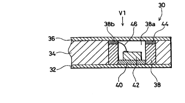
Fig. 2 is a seci;ional view taken along sectional plane II-II of Fig. 1.
Fig. 3 is a plan view of IC card 3 viewed from the direction of Vl of
Fig. 2 with a surface layer member 3G removed.
Fig. 4 is sectional view showing a sectional structure of a non-contact
type IC card 50 according to another embodiment of the present invention.
Fig. 5 is a sectional view showing a sectional structure of a non-
contact type IC card 170 according to a further embodiment of the present
invention.
-5/1-
CA 02277181 1999-06-25
Fig. 6 shows the appearance of a non-contact type IC card 60
according to still anather embodiment of the present invention.
Fig. 7 shows an example of a conventional non-contact type IC card.
Fig. 8A is a sectional view taken along line VIVA-VIIIA of Fig. 7) and
Fig. 8B is a circuit diagram of IC card 2.
Best Modes for Carrying Out the Invention
Fig. 1 shows an appearance of a non-contact type IC card 30 as a
circuit chip mounted card according to an embodiment of the present
invention. IC card 30 is a one-coil type IC card used in the automatic
examination for a ski lift at skiing grounds and railways, automatic sorter
of parcels) and the like.
Fig. 2 is a sectional view taken along line II-II of Fig. 1. IC card 30
has a structure of sequential layers of a surface layer member 32 which is
the first substrate) a core member 34, and surface layer member 36 which
is the second substrate. Synthetic resin such as vinyl chloride, PET
(polyethylene terephthalate) and the like are used for surface layer
members 32 and 36. Core member 34 is formed of synthetic resin.
A ceramic frame 38 is embedded in the layer formed of core member
34. Cer amic frame 38 is formed of ceramic in a cylindrical configuration.
Cer amic frame 38 carresponds to the frame of a reinforcing body. In the
present embodiment:, the reinforcing body is formed only of the frame.
~'he interior 38a of ceramic frame 38 forms a cavity. An elastic
member 40 which is a buffer member is layered in contact with surface
layer member 32 at the bottom end of interior 38a of ceramic frame 38.
Adhesive silicon rubber is used for elastic member 40. An IC chip 42
which is the circuit chip is supported on elastic member 40. In the present
embodiment, a capacitor for a resonant circuit and a capacitor for
smoothing the power source are incorporated in IC card 42.
By embedding ceramic frame 38 in the layer of core member 34, the
bending rigidity) torsion rigidity) and compression rigidity of IC card 30 in
the proximity of ceramic frame 38 can be improved significantly.
Even if a strong bending, torsional) or pressing force is exerted on
the IC card, IC chip 42 located at interior 38a of ceramic frame 38 will not
-6-
CA 02277181 1999-06-25
be greatly deformed. Therefore, damage of IC chip 42 will seldom occur
even when a bending) torsional, or pressing force and the like is exerted.
In other words, the reliability of IC card 30 can be improved.
By fixing IC chip 42 via elastic member 40, any impact on IC card 30,
when exerted) will not be directly transmitted to IC chip 42. Therefore,
the damage of IC chip 42 caused by an impact can be alleviated.
In the present; embodiment, the thickness of both surface layer
members 32 and 36 :is O.lmm) and the entire thickness of IC card 30 is
0.768mm. IC chip 42 is a square having the sides of 3mm in length and
0.25mm in thickness. Elastic member 40 has a thickness of 0.118mm.
The height of ceramic frame 38 is 568mm including a coil 44 that will be
described afterwards) adjacent to an upper end face 38b. - The inner
diameter of ceramic frame 38 is set so that the clearance from the
incorpor ated IC chip 42 is approximately 0.2-0.3mm. The outer diameter
of ceramic frame 38 :is approximately 23mm. It is to be noted that the
present invention is not limited to these dimensions and materials.
Coil 44 forming an antenna is provided at the upper end of ceramic
frame 38. Fig. 3 shows IC card 30 viewed from the direction of Vl of Fig. 2
with suuace layer member 36 removed. Coil 44 is formed of a looped
metal wire provided by printing or etching on upper end face 38b of
cylindrical ceramic frame 38. The terminal of coil 44 is connected to IC
chip 42 by a wire 46..
The provision of coil 44 at upper end face 38b of ceramic frame 38
allows the preparation in advance of a unitary element of the connection of
IC chip 42) ceramic flame 38 and coil 44. Therefore, the fabizcation cost
can be reduced by virtue of improvement in the workability of fabrication.
Since wire 46 connecting IC chip 42 and coil 44 is located within the
range of highly rigid ceramic frame 38, cut off or disconnection of wire 4G
caused by IC card 30 being bent is less likely to occur. Therefore, the
reliability of non-contact type IC card 30 including coil 44 can be improved.
By forming th.e reinforcing body with ceramic, high rigidity can be
obtained. It is not necessary to use an insulator in providing coil 44 at
ceramic flame 38 by virtue of the high insulation of the ceramic. Coil 44
?_
CA 02277181 1999-06-25
can be directly provided at ceramic frame 38 by printing and the like to
reduce the fabrication cost.
The operation of IC card 30 is similar to that of conventional IC card
2. More specifically, an electromagnetic wave sent from a reader/writer
(write/read device, not shown) is received by a resonant circuit (not shown)
formed of coil 44 and a capacitor (not shown) incorporated in IC chip 42.
The received electromagnetic wave corresponds to the power source. A
capacitor (not shown) for smoothing the power is incorporated in IC chip 42.
The obtained information overlapped with the electromagnetic wave
is decoded by a control unit (not shown) provided in IC chip 42. The
decoded information is sent back. This response is effected by altering the
impedance of the resonant circuit. The readerlwriter can identify the
contents of the response by detecting the impedance change of its own
r esonant circuit (not shown) in actor dance with the impedance change of
the resonant circuit of IC card 3.
Thus, information can be transmitted/received with the card absent
of a power source, and in a non-contact manner.
Although the above embodiment is configured so that IC chip 42 is
fixed to surface layer member 32 via elastic member 40 as shown in Fig. 2,
IC chip 42 can be directly fixed to surface layer member 32 without elastic
member 40.
Fig, 4 shows a sectional view of a non-contact IC card 50 as a circuit
chip mounted card according to another embodiment of the present
invention. The appearance of the structure of IC car d 50 is similar to that
of IC card 30 (refer to Fig. 1). The view from Vl of Fig. 4 is substantially
similar to that for IC card 32 (refer to Fig. 3).
It is to be noted that the configuration of ceramic frame 52 in IC card
50 as shown in Fig. 4 differs from that of ceramic frame 38 of IC card 32
(refer to Fig. 2). More specifically, ceramic frame 52 differs from ceramic
fi ame 38 formed only of a cylindrical frame body in that it includes a
cylindrical section 52a which is a frame body, and a bottom section 52b
which is tabular provided integrally continuous to the lower end of
cylindrical section 52a.
_g_
CA 02277181 1999-06-25
As shown in Fig. 4) IC chip 42 is configured to be directly fixed to
bottom section 52b of recess cavity 52c formed by cylindrical section 52a
and bottom section 52b of ceramic frame 52.
By providing a bottom section 52b integrally continuous to the lower
end of cylindrical section 52a, the rigidity of ceramic frame 52 can be
further improved. Therefore, the desired rigidity can be ensured even
when the dimension of ceramic frame 52 in the plane direction (the X
direction and Y direction in Fig. 1) is relatively increased. Therefore, the
diameter of coil 44 can be set greater.
As shown in Fig. 4, IC chip module 54 which is the circuit chip
module is formed of ceramic frame 52) IC chip 42 fixed to ceramic frame 52,
coil 44 formed by being panted or etched at ceramic frame 52, and wire 46
connecting coil 44 and IC chip 42. By providing such a module, the
workability in the fabrication process can be improved to allow reduction in
the fabrication cost.
Although the present embodiment is configured so as to directly fix
IC chip 42 at bottom. section 52b of ceramic frame 52, an elastic member 40
as shown in Fig. 2 can be provided between IC chip 42 and bottom section
52b of ceramic frame 52. Accordingly, the impact exerted on the card can
be alleviated.
Each of the above embodiments is configured so as to form coil 44 at
the upper end face of ceramic frame 38 or 52. However) the coil can be
provided at the lower end, side plane) or both ends of ceramic frame 38 or
52. Furthermore, ceramic frame 38 or 52 can be divided into two or more
pieces in the thickness direction so as to sandwich the coil between the
divided ceramic frames.
Although coil 44 is directly formed at ceramic frame 38 or 52 by
printing or etching, a coil can be formed by etching and the like at a
synthetic resin film and connect that film formed with a coil to ceramic
frame 38 or 52. Furthermore) the coil can be wound around ceramic frame
38 or 52.
Fig. 5 shows a sectional structure of a non-contact type IC card 170
which is a circuit chip mounted card according to another embodiment of
-9-
CA 02277181 1999-06-25
the present invention. The appearance of IC card 170 is similar to that of
IC card 30.
As shown in Fig. 5, the configuration of ceramic frame 172
corresponding to a fr. ame body in IC card 170 differs from ceramic frame 38
(refer to Fig. 2) in IC, card 30. More specifically) ceramic frame 172 has the
outer side formed of a unit cylinder, likewise ceramic frame 38, and the
inner side formed in a stepped cylindrical shape.
As shown in F'ig. 5, a stepped portion 172a of ceramic dame 172 has
a coil 44 formed functioning as an antenna. A support film 174 forming a
buffer member is arranged on coil 44. Support film 1?4 is a synthetic
resin film formed as a hollow cylinder with a panted wiring (not shown)
applied. The printed wiring of support film 174 and a terminal 44a
provided at the end of coil 44 are coupled by soldeizng or bumping
technology (terminal junction technique) and the like. Therefore, support
film 174 is supported in a resting manner on step portion 172a of ceramic
frame.172 via coil 44 within inner cavity 172b of ceramic frame 172.
An IC chip 42 is provided substantially at the center of support film
174. The printed wiring of support frame 174 and terminal 42a of IC chip
42 are coupled by soldering or bumping techniques. Therefore, IC chip 42
is supported by support film 174 in a suspending manner within internal
cavity 172b of ceramic frame 172.
Terminal 44a of coil 44 and terminal 42a of IC chip 42 are
electrically connected through the aforementioned printed wiring provided
at support film 174.
By such a structure, an impact exerted on the card can be reliably
alleviated. No wire is required in electrically connecting coil 44 and IC
chip 42. Therefore, the event of disconnection or cut off of the wir a will
not
occur. As shown in. Fig. 5) ceramic frame 172, coil 44) suppoW film 174 and
IC chip 42 form IC chip module 176 as a circuit chip module. By such a
modular form, the workability in fabrication is improved to reduce the
fabizcation cost.
The present embodiment is configured so as to connect the printed
wiring of support film 174 with terminal 42a of IC chip 42 by means of
-10-
CA 02277181 1999-06-25
soldering or bumping techniques. However, support film 174 and IC chip
42 can be coupled via an isotropic conductor (not shown). An anisotropic
conductor is a conductor having conductivity in only one direction, and is
adhesive. Anisolum (Hitachi Chemical Company Limited) that is a
thermosetting adhesive can be used as the anisotropic conductor.
The usage of such an anisotropic conductor allows the printed wiring
of support film 174 to be electrically connected to terminal 42a of IC chip
42.
Since the anisotropic conductor is applied so as to fill up the gap between
support film 174 and IC chip 42, the bonding strength between support film
174 and IC chip 42 can be increased significantly. By the formation of
entirely covering top surface 42b of IC chip 42 by the anisotropic conductor,
introduction of moisture into IC chip 42 can be prevented. Therefore,
corrosion of the aluminum wiring (not shown) in IC chip 42 can be
prevented.
According to the present embodiment, printed wiring is provided at
support film 174 and. electrical connection established between coil 44 and
IC chip 42 via the printed wiring. However, coil 44 and IC chip 42 can be
electrically connected via a wire as in the embodiment shown in Figs. 2 and
4. Although a synthetic resin film of a hollow cylindrical shape is used as
the buffer member, the shape and the material of the buffer member are
not limited to the aforementioned.
Coil 44 is provided at a stepped section 172a of ceramic frame 172 in
the present embodiment. However, coil 44 can be provided at the top
surface, bottom surface) side surface, end surface and the like of ceramic
frame 172. Also, ceramic frame 172 can be divided into two or more pieces
in the direction of the thickness, and insert the coil between the divided
ceramic frames.
Coil 44 is formed at ceramic frame 172 by printing or etching.
However, the coil can be directly formed by a printed wising and the like at
support film 174. Also) the coil can be round around ceramic frame 172.
Furthermore, coil 64 can be provided external to ceramic flame 62 as
in an IC card 60 of Fig. 6. Such a structure allows coil 64 to be increased
in size without increasing the dimension of ceramic frame 62. Therefore,
-11-
CA 02277181 1999-06-25
information can be transmitted/received even when the distance from the
reader/writer is great.
A through cylindrical or a cylinder with a bottom is used as the
reinforcing body in each of the above embodiments. However, the outside
or inside configuration of the cylinder is not limited to the cylinclizcal
shape.
For example, a rectangular tubular form can be used as the reinforcing
body. Also, the reinforcing body is not limited to a cylinclizcal form, and a
tabular form, for example, can be used. Furthermore) a plugality of
reinforcing bodies can be provided. For example) a reinforcing body can be
provided above and below so as to sandwich the circuit chip.
The reinforcing body is formed of ceramic in each of the above
embodiments. However, a material other than ceramic can be used as long
as it is rigid. For example, a metal material such as stainless steel or hard
synthetic resin and the like can be used.
The capacitor for a resonant circuit and the capacitor for power
smoothing are incorporated in IC chip 42 in each of the above embodiments.
However, these capacitors do not have to be incorporated in IC chip 42. In
such a case, IC chip 42 and the capacitor are mounted on a tab) which is
installed within ceramic frame 38 or 52) as shown in Fig. 8A. In the
embodiment of Fig. !i, the capacitor can be mounted at support film 174.
Each of the above-described embodiments is exemplified with the
present invention applied to a one-coil type non-contact IC car d. However)
the present application is also applicable to the so-called multi-coil type
non-contact IC card. Furthermore) the present invention is applicable to a
contact type IC card besides the non-contact type IC card. Furthermore)
the present invention is applicable to the entire module incorporating the
circuit chip and the entire card in addition to an IC card. Here) a card
implies a substantially tabular member, such as a credit card, a
commutation ticket, a common ticket of the railway, and the like.
-12-