Note: Descriptions are shown in the official language in which they were submitted.
CA 02277322 1999-07-09
SWITCHING APPARATUS OF TIME DIVISION MULTIPLEXING
SYSTEM FOR CONTROLLING DATA TRANSMISSION THROUGH
MESSAGE MEMORY SHARED BETWEEN PLURAL CHANNELS,
METHOD FOR DATA TRANSMISSION AND INFORMATION STORAGE
MEDIUM FOR THE METHOD
This invention relates a to a time division multiplexing system and, more
particularly, to a switching apparatus incorporated in the time division multi-
plexing system for controlling the data transmission, a method for controlling
the data transmission and an information storage medium storing a program
sequence for the method.
Conventionally, the switching apparatus is connected to a message line,
and messages are transferred from the switching apparatus to the message line
through a time division multiplexing. Time on the message line is divided
into frames, and each frame is further divided into time slots. A time slot
starts at a certain timing in one of the frames, and forms a channel together
with the time slots at the same timing in the other frames. The messages are
not constant in length. A message may require the time slots different from
those to be required for another message. The message is divided into pieces,
and the pieces of message are assigned to the time slots of a channel.
1
CA 02277322 1999-07-09
The prior art switching apparatus includes message memories for storing
the messages and message transmitters for delivering the messages to the
channels. Each of the message memories is exclusively used for one of the
channels, and the message transmitters are also assigned the channels, re-
spectively. Thus, the prior art switching apparatus requires plural combina-
dons of the message memories and the message transmitters equal in number
to the channels. This feature is uneconomical. The message memories and
the message transmitters increase the production cost of the prior art switch-
ing apparatus. Thus, a problem inherent in the prior art switching apparatus
is the high production cost.
It is therefore an important object of the present invention to provide a
switching apparatus, which is low in production cost.
It is also an important object of the present invention to provide a method
for transferring messages in a time division multiplexing fashion which is re-
peated in the switching apparatus.
It is also an important object of the present invention to provide an infor-
mation storage medium for readably storing programmed instructions for the
method.
To accomplish the object, the present invention proposes to share a mes-
sage memory between channels.
In accordance with one aspect of the present invention, there is provided a
switching apparatus for supplying pieces of data information to plural chan-
2
CA 02277322 1999-07-09
nets defined on a data line through a time division multiplexing comprising a
first memory having first memory areas storing first pieces of data informa-
tion to be selectively transferred to the plural channels and responsive to a
first address signal for selectively outputting the first pieces of data
informa-
tion, a second memory having second memory areas storing second pieces of
data information to be selectively transferred to the plural channels and re-
sponsive to a second address signal for selectively outputting the second
pieces of data information, a selector connected between the first and second
memories and the data line and responsive to a control signal so as to selec-
tively transfer the first pieces of data information and the second pieces of
data information to the plural channels, a channel controller including a
third
memory having third memory areas associated to the plural channels, respec-
tively, and storing pieces of address information each assigned to one of the
first memory areas for storing one of the first pieces of data information to
be
transferred to associated one of the plural channels or one of the second
memory areas for storing one of the second pieces of data information to be
transferred to the associated one of the plural channels together with first
pieces of flag information each used for controlling the data transfer from
the
first and second memories to associated one of the plural channels and a con-
troller connected to the first memory, the second memory, the third memory
and the selector, and sequentially accessing the third memory areas for con-
trolling the data transfer from the first and second memories through the se-
3
CA 02277322 1999-07-09
lector to the output line with the control signal, the first address signal
and
the second address signal.
In accordance with another aspect of the present invention, there is
provided a method for transferring pieces of data information to plural chan-
nels through a time division multiplexing comprising the steps of a) storing
first pieces of data information, second pieces of data information and plural
combinations of pieces of address information and first pieces of flag infor-
mation in first memory areas of a first memory, second memory areas of a
second memory and third memory areas of a third memory, respectively, b)
deciding a timing to be given for a data transfer to one of the plural
channels,
c) checking one of the third memory areas assigned to the aforesaid one of the
plural channels to see whether the first piece of flag information is
indicative
of a data transfer from the first memory to the aforesaid one of the plural
channels or from the second memory to the aforesaid one of the plural chan-
nels and d) instructing either first memory or second memory to transfer one
of the first pieces of data information or one of the second pieces of data in-
formation to the aforesaid one of the plural channels.
In accordance with yet another aspect of the present invention, there is
provided an information storage medium for storing a set of programmed in-
structions representative of a method for transferring pieces of data informa-
tion to plural channels through a time division multiplexing comprising the
steps of a) storing first pieces of data information, second pieces of data in-
formation and plural combinations of pieces of address information and first
4
CA 02277322 1999-07-09
pieces of flag information in first memory areas of a first memory, second
memory areas of a second memory and third memory areas of a third memory,
respectively, b) deciding a timing to be given for a data transfer to one of
the
plural channels, c) checking one of the third memory areas assigned to the
aforesaid one of the plural channels to see whether the first piece of flag in-
formation is indicative of a data transfer from the first memory to the afore-
said one of the plural channels or from the second memory to the aforesaid
one of the plural channels and d) instructing either first memory or second
memory to transfer one of the first pieces of data information or one of the
second pieces of data information to the aforesaid one of the plural channels.
The features and advantages of the switching apparatus, the method and the
information storage medium will be more clearly understood from the fol-
lowing description taken in conjunction with the accompanying drawings in
which:
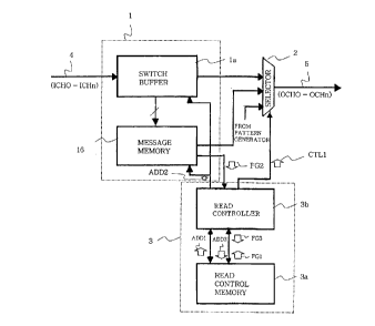
Fig. 1 is a block diagram showing the arrangement of a switching appara-
tus incorporated in a time division multiplexing system according to the pre-
sent invention;
Fig. 2 is a view showing plural memory areas defined in a switch buffer
1 a;
Fig. 3 is a view showing plural memory areas defined in a message memo-
ry unit;
CA 02277322 1999-07-09
Fig. 4 is a view showing plural memory areas defined in a read control
memory; and
Fig. 5 is a flow chart showing a program sequence executed by a read
controller incorporated in the switching apparatus.
Referring to figure 1 of the drawings, a switching apparatus embodying
the present invention largely comprises a memory unit 1, a data transmitter 2
and a channel controller 3. The switching apparatus is incorporated in a time
division multiplexing system. An input message line 4 is connected to the
memory unit 1, and the data transmitter 2 is connected to an output message
line 5. Input channels and output channels are respectively defined on the in-
put message line 4 and the output message line 5 as similar to the prior art.
The input channels are respectively assigned to different messages, and each
of the messages is represented by an input data byte or input data bytes.
Similarly, the output channels are respectively assigned to the messages, and
one of the output messages is represented by output data bytes. The messages
are temporarily stored in the memory unit 1, and are delivered from the data
transmitter 2 to the output channels under the control of the channel
controller
3. In this instance, the input message line 4 and the output message line 5
are
assumed to have n+1 input channels ICHO- ICHn and n+1 output channels
OCHO- OCHn, respectively.
The memory unit 1 includes a switch buffer la and a message memory lb.
Plural addressable memory areas M10/ M11/ .../ Mln are defined in the
6
CA 02277322 1999-07-09
switch buffer la, and are assigned to the input data bytes transferred through
the input channels ICHO- ICHn, respectively, as shown in figure 2. The data
bytes stored in the addressable memory areas M10- Mln are representative of
pieces of different messages "0" - "n".
The message memory lb includes plural addressable memory areas M20/
M21/ ... / M2k/ 2K+1/ ... / M2j/ ... ., and each addressable memory areas has
a
data sub-area 1c assigned to the data byte representative of a piece of
message
and a flag sub-area ld assigned to an end flag bit E representative of the
final
data byte of a message as shown in figure 3. If the data byte is non-final,
the
end t7ag bit E is "0". When a final data byte is stored, the final data byte
is
labeled with the end t7ag bit E of "1". The input channels ICHO/ ICH1 are as-
sumed to supply message "0" represented by k+1 data bytes and the message
"1" represented by j+1 data bytes to the memory unit 1. The data byte 0 to
the data byte k are respectively stored in the memory areas M20- M2k, and
data byte 0 to the data byte j are respectively stored in the memory areas
M2k+1 - M2j. The data bytes 0 to k-1 representative of the pieces of message
"0" are non-final, and the end flag bit E is "0". However, the data byte k is
representative of the final piece of the message "0", and is labeled with the
end flag bit E of "1". Similarly, the data bytes 0 to j-1 are non-final, and
are
labeled with the end flag bit E "0". The data byte j is the final byte for the
message "1", and is labeled with the end flag bit E "1". Thus, the final data
bytes of the messages are discriminative with the end flag bit E of "1".
7
CA 02277322 1999-07-09
If the data bytes are not transferred from the switch buffer la through the
data transmitter 2 to the output message line S, they are supplied to the mes-
sage memory lb upon completion of each frame, and are written into the mes-
sage memory 1b under the control of a controller (not shown) incorporated in
the switching apparatus. As a result, the message memory lb stores the data
bytes of a message or messages not delivered to the output message line 5 yet.
The data transmitter 2 is implemented by a selector, and the selector 2 is
connected to three data sources, i.e., the switch buffer la, the message mem-
ory 1b and a pattern generator (not shown). The pattern generator supplies a
data byte representative of an idling pattern to the selector 2. The selector
2
is responsive to a control signal CTLl so as to selectively transfer the data
byte from the three data sources to the output message line 5.
Turning back to figure 1, the channel controller 3 includes a read control
memory 3a and a read controller 3b. The read control memory 3a includes
plural memory areas M30- M3n as shown in figure 4. The memory areas
M30- M3n are respectively assigned to the output channels OCHO- OCHn,
and are divided into a data sub-area 3c and a flag sub-area 3d. Pieces of ad-
dress data are stored in the data sub-area 3c, and flag bits C/ S/ I/ SYNC are
stored in the flag sub-area 3d. Each piece of address data is indicative of an
address assigned to one of the memory areas M10- Mln or a memory area for
storing the origin of the message such as, for example, the data byte 0 of the
message "0".
8
CA 02277322 1999-07-09
The flag bit C is indicative of the permission to access the message mem-
ory lb or the prohibition from the access to the message memory 1b.
The flag bit S is indicative of whether the data byte or bytes stored in the
message memory lb are valid or invalid. If the flag bit S is "1 ", the data
bytes in the message memory lb are valid, and the message has not been de-
livered to the output channel, yet. On the other hand, if the final data byte
is
delivered to the output channel, the flag bit S is changed to "0".
The flag bit I is indicative of the idling pattern to be delivered to the out-
put channel. If the flag bit I is "1", the read controller 3b produces the con-
trol signal CTLl indicative of the idling pattern, and supplies the control
sig-
nal CTL1 to the selector 2. This means that the read controller 3b selects the
switch buffer 1a on the basis of the remaining combination of the flag bits S
and I, i.e., S = 0 and I = 0. In this instance, the flag bit S has the
priority to
the flag bit I as will be described hereinlater.
Although the flag bit SYNC is not used in this instance, the flag bit SYNC
is changed between an active level and an inactive level. When the flag bit
SYNC is in the active level, the read controller 3b is requested to make the
data transfer in synchronism with an external signal. In other words, the read
controller 3b ignores the flag bit C until the external signal is changed to
ac-
tive.
The read controller 3b accesses the read control memory 3a in synchro-
nism with the time slots in each frame, and sequentially fetches the pieces of
address data and the flag bits C/ S/ I from the memory areas M30- M3n for
9
CA 02277322 1999-07-09
transferring the data bytes to the time slots of the output channels OCHO-
OCHn. The pieces of address data and the flag bits C/ S/ I are supplied from
the read control memory 3a through an address signal ADD1 and a flag signal
FG1 to the read controller 3b. The read controller 3b selectively enables the
switch buffer la and the message memory lb, and supplies the address signal
ADD1 to selected one of the switch buffer la and the message memory lb.
The read controller 3b gives the control signal CTLl a value representative of
one of the three data sources, and causes the selector 2 to connect the
selected
data source to the output message line 5. The read controller 3b fetches the
end flag bit E from the message memory lb, and increments the address by
one. The read controller 3b writes the new address into the read control
memory 3a through an address signal ADD3. The read controller 3b fetches
the end flag bit E through a flag signal FG2 to see whether the data transmis-
sion for a message is completed or not. When the data transmission is com-
pleted, the read controller 3b changes the flag bit S through a flag signal
FG3.
The read controller 3b repeats a program sequence shown in figure 5 so as
to deliver the data bytes representative of the messages "0" - "n" to the
output
channels OCHO- OCHn. In other words, the read controller 3b once executes
the program sequence for one of the output channel, and repeats it for the oth-
er output channels. In the following description, the read controller 3b is as-
sumed to execute the program sequence for the output channel OCHO. In or-
der to make the description simple, the data transmission is described as if
all
CA 02277322 1999-07-09
the data bytes 0 to k are transferred to the output channel 0 without any
inter-
ruption.
The read controller 3b checks the time to see whether or not the timing for
the output channel OCHO comes as by step S1. If the answer at step Sl is
given negative, the read controller 3b waits for the timing by repeating the
step S1. When the timing for the output channel OCHO comes, the answer at
step S1 is changed to affirmative, and the read controller 3b proceeds to step
S2.
The read controller 3b accesses the memory area M30 at step S2, and reads
out the piece of address data and the flag bits S/ I from the memory area M30
through an address signal ADD2 and a flag signal FG1. The read controller
3b checks the flag bit S to see whether the message "0" in the message mem-
ory lb is valid or invalid as by step S3. If the flag bit S is "1", the
message
"0" is valid, and the answer at step S3 is given affirmative. Then, the read
controller 3b makes the message memory lb accessible, and supplies the ad-
dress signal ADD2 indicative of the head address of the memory area 20 to
the message memory lb. The read controller 3b supplies the control signal
CTLl indicative of the message memory lb to the selector 2, and the selector
2 becomes ready for transferring the data byte from the message memory lb
to the output channel OCHO. The message memory lb is responsive to the
address signal ADD2 so as to supply the data byte 0 and the end flag bit E "0"
to the selector 2 and the read controller 3b, respectively, as by step S4. The
data byte 0 is transferred to the output channel OCHO. The end flag bit E is
11
CA 02277322 1999-07-09
transferred from the message memory lb to the read controller 3b through the
flag signal FG2.
The read controller checks the end flag bit E to see whether the read-out
data byte is final or non-final as by step S5. The data byte 0 is labeled with
the end flag bit E "0", and the end flag bit E "0" indicates that the data
byte 0
is non-final. Then, the answer at step SS is given negative, and the read con-
trolley 3b increments the address represented by the piece of address data as
by step S6. The read controller 3b writes the piece of address data represen-
tative of the new address into the memory area M30 through the address sig-
nal ADD3 as by step S7. The piece of address data is now indicative of the
head address of the memory area M31.
The read controller 3b repeats the loop consisting of steps S1 to S7 until
the data byte k is transferred to the selector 2. The data byte k is labeled
with
the end flag bit E of "1", and the answer at step SS is changed to
affirmative.
Then, the read controller 3b proceeds to step S8, and changes the flag bit S
to
zero through the flag signal FG3. The flag bit S indicates that the message
"0" is invalid, and does not permit the read controller 3b to transfer the mes-
sage "0" to the output channel OCHO twice. Thus, the switching apparatus
completes the data transmission of the message "0" from the message memory
lb to the output channel OCHO through repetition of the loop consisting of
steps S1 to S8.
On the other hand, if the flag bit S is zero, the message "0" is invalid, and
the answer at step S3 is given negative. Then, the read controller 3b proceeds
12
CA 02277322 1999-07-09
to step S9. The read controller 3b checks the flag bit I to see whether or not
the idling pattern should be transferred to the output channel OCHO. When
the flag bit I is "0", the switch buffer 1a stores a data byte to be
transferred to
the output channel OCHO, and the answer at step S9 is given negative. Then,
the read controller 3b makes the switch buffer la accessible, and supplies the
address signal ADD2 representative of the head address of the memory area
M10 to the switch buffer la. Concurrently, the read controller 3b changes the
control signal CTLl to a value representative of the switch buffer la, and
supplies the control signal CTL1 to the selector 2. The switch buffer la sup-
plies the input data byte from the memory area M10 to the selector 2, and the
selector 2 transfers the data byte to the output channel OCHO as by step S10.
On the other hand, if the flag bit I is "1 ", there is not any data byte to be
transferred to the output channel OCHO, and the answer at step S9 is given af-
firmative. The read controller 3b changes the control signal CTLl to a value
representative of the pattern generator (not shown), and supplies the control
signal CTL1 to the selector 2. The selector 2 transfers the idling pattern to
the output channel OCHO as by step S11.
Upon execution of one of the steps S7/ S8/ S10/ S11, the read controller
3b returns to step S1, and repeats the program sequence for the data transfer
to the output channel OCHO. As described hereinbefore, the above-
description is made on the assumption that the data transfer is performed for
the output channel OCHO. The read controller 3b also executes the program
sequence S1 to S11 for each output channel OCH1- OCHn.
13
CA 02277322 1999-07-09
A set of instruction codes represents the program sequence shown in figure
5, and is stored in an information storage medium such as, for example, a hard
disk incorporated in or associated with the read controller 3b. The set of in-
struction codes may be supplied to a built-in memory of the read controller 3b
through a communication network.
As will be understood from the foregoing description, the read controller
3b is associated with the read control memory 3a, and the control memory 3a
stores the flags and the addresses for the data bytes to be transferred to the
plural output channels OCHO- OCHn. This feature is desirable, because the
message memory 1 is shared between the output channels OCHO- OCHn.
This results in the simple memory unit 1. The simple memory unit 1 reduces
the production cost of the switching apparatus.
Even though the messages are different in length, the end flag bit E teaches
the read controller 3b the final data byte, and the message memory lb can
store variable-length messages.
Although a particular embodiment of the present invention has been shown
and described, it will be apparent to those skilled in the art that various
changes and modifications may be made without departing from the spirit and
scope of the present invention.
For example, when the final data byte is transferred from the message
memory lb to the associated output channel, the read controller 3b may ter-
urinate the data transmission by using the flag bit C instead of the flag bit
S.
14
CA 02277322 1999-07-09
The t7ag C may indicate the data source to be accessed, i.e., the switch
buffer la, the message memory lb or the pattern generator. When the flag C
is set to value "1", the switch buffer 1a supplies the data byte to the
selector 2.
The message memory lb is indicated by the flag C of "2", and the pattern
generator is indicated by the flag C of "3".
One than one byte may be stored in the memory area M20- M2j.