Note: Descriptions are shown in the official language in which they were submitted.
CA 02277422 1999-07-09
TOPOLOGY-INDEPENDENT PRIORITY ARBITRATION
FOR STACRAHLE FRAME SWITCHES
Technical Field
This invention provides a priority arbitration
mechanism for selecting a "master" frame switch from a
plurality of atacked frame switches. The mechanism is
independent o:E the topology used to interconnect the
switches.
Background
"Stackable" Ethernet switches are emerging as a
possible alternative to chassis-based modular Ethernet
switches, offering some of the same expandability and
unified management capabilities as chassis-based systems
without the concomitant start-up cost and configuration
problems. These switches usually consist of one or more
identical boxes, "stacked" one on top of another, and
interconnected by means of cables carrying Ethernet packet
data as well as control information. Switches intercon
nected in thi:~ fashion perform as a single entity (with
respect to management protocols) rather than as a collec
tion of isolated units. This simplifies the network
manager's task by facilitating presentation of a unified
view of a large network.
Each of the individual units constituting a stack
of switches normally contains a stack controller central
processing unit (CPU) that serves to configure and manage
the system. Because the individual units are identical, a
stacked system contains multiple stack controller CPUs. It
is necessary to prevent conflicts and contention among the
multiple CPUs by allowing only one CPU to function as a
controller (for the entire stack) at a time, and by pre-
venting the other CPUs from interfering with the management
operations. Support for stackable switches thus typically
involves implementing some means whereby only one of
several CPUs :in the stack is permitted to operate at a
time.
CA 02277422 1999-07-09
- 2 -
It is possible to manually select a particular
stack controller CPU to act as the overall stack control-
ler, or "mast:er". However, this can create problems
stemming from 'user error or CPU failure. It is preferable
to implement some farm of autonomous process whereby each
of the multiple stack controller CPUs contend with one
another in an "'election" or priority arbitration scheme for
control of thEa stack, with a single "winner" being per-
mitted to assume stack mastership and perform the required
configuration and management operations. This has the
further advantage of allowing an automatic switchover of
mastership from one CPU to another in the event of a CPU
failure. Thus, if a previously determined "winner" fails
during operation, then a new "winner" can be automatically
"elected", wit.hout human intervention, to take over the
management of 'the stack.
Current implementations of stackable switches use
some form of auxiliary hardware, requiring special connec-
tions or support logic, to resolve contention between
multiple stack controller CPUs in a single system. This
has the disadvantage of increased cost, as well as render-
ing the election process dependent on the specific system
topology (i.e., the pattern of interconnections between
units in a st:ack). In addition, these approaches are
difficult to scale, and hence restrict the number of units
that may be placed in a single stack. Examples of such
prior art implementations include "Futurebus+ Logical
Protocol Specification", ISO/IEC 10857:1994 (IEEE 896.1,
1994); and, The Philips Semiconductors "12C-Bus Specifica-
tion", Version 2.0, December, 1998.
A preferable priority arbitration process for
implementing the stack controller CPU election process
should satisfy the following objectives:
1. The proce ss must be completely automatic, requiring no
manual intervention or configuration.
2. The process must function properly with unknown stack
interconnect topologies, because the topology may be
CA 02277422 1999-07-09
- 3 -
unknown a.t the time that a stack controller CPU is
required to begin performing its duties.
3. The proce:~s must support automatic switchover from any
"winner" stack controller CPU to a backup CPU if the
"winner" CPU fails for any reason during switch
operation.
4. The process must be capable of dealing with the
addition or removal of new stack controllers at random
times without failure. This may occur, for example,
as individual units within the same stack are powered
on at slightly varying intervals, or when a new unit
is added i.o a stack and interconnected to the existing
units.
5. The process must be robust in the face of errors, and
must not rely on any precise timing relationships
between signals in different units in the stack. In
particular, the process should not rely on any cen
tralized mechanism, but should use a completely
distributed approach to avoid creating a single point
of failure that could potentially prevent a backup CPU
from taking over from a failed CPU.
6. The process algorithm should be simple and reliable,
and the implementation should not be expensive in
terms of :hardware or bandwidth resources.
7. The procEass algorithm should be capable of being
implemented without consuming a large amount of
interconnect bandwidth (in the form of additional
physical interconnects, or data transfer capacity
within existing interconnects) during the arbitration
process.
The present invention satisfies the foregoing objectives.
Summary of Invention
The invention provides a topology-independent
priority arbitration mechanism for realizing the stack
controller arbitration process, and is preferably imple
mented as a combination of hardware and software. The
CA 02277422 1999-07-09
- 4 -
hardware perfarms basic, primitive operations respecting
the transfer of individual bits of information between
stack controller CPUs. The software utilizes the hardware
to perform the actual priority arbitration process and
"elect" a single CPU to be the "master" of the stacked
system.
The priority arbitration mechanism is implemented
in a distributed manner, with each stack controller CPU
running an identical copy of the software and possessing an
identical set of hardware resources. This eliminates the
possibility of a single point of failure that would prevent
a backup CPU from taking over "mastership" of the stack in
the event of a catastrophic failure of the current stack
master. To deal with the situation where the currently
elected stack controller CPU is removed from the stack
(either by system failure, or by the removal of the unit
containing the CPU), the priority arbitration procedure is
continuously repeated while the stack is powered on. A
resolution mechanism is provided to determine when a backup
stack controller CPU should be allowed to assume mastership
if the current stack master is no longer present, or is not
functioning. In addition, this simplifies the process of
dealing with the insertion or removal of units containing
stack controller CPUs at arbitrary times; the removal of a
unit may be 'treated equivalently to the failure of a
controller, and no special considerations are required to
handle this event.
The general architectural model within which the
priority arbitration mechanism is expected to operate is
that of a set of stack controller CPUs (typically, one CPU
is located within one unit within the stack) interconnected
by means of a switching fabric. The fabric is required to
switch data from one physical port to another, to fulfil
the functions of a network switching system. The priority
arbitration mechanism consumes a very small portion of the
transfer bandwidth of the switching fabric in order to
CA 02277422 1999-07-09
- 5 -
transfer control information between CPUs and implement the
controller arbitration algorithm.
Brief Description of Drawings
Figure lA is a block diagram illustration of a
star stacking topology for interconnecting stacked Ethernet
switches.
Figure 1B is a block diagram illustration of a
bus stacking topology for interconnecting stacked Ethernet
switches.
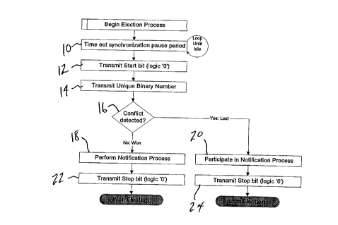
Figure 2 is a flowchart illustrating the basic
procedural steps in a priority arbitration process for
implementing a stack controller CPU arbitration process in
accordance with the invention.
Figures 3, 4 and 5 are flowcharts which respect
ively illustrate the procedural steps of the synchroniz
ation, ID broadcast, and trailing synchronization sequence
phases of a priority arbitration process for implementing
a stack controller CPU arbitration process in accordance
with the invention.
Description
In t:he EXACTTM Ethernet system, the switching
fabric is realized using dedicated silicon devices inter
connected in a variety of ways. In addition, the inter
faces between the physical Ethernet ports and the switching
fabric are contained within other hardware devices called
"port controllers". The port controllers implement special
hardware functions that permit the stack controller CPUs to
exchange information over the switching fabric.
Figures 1A and 1B depict two exemplary configur-
ations of the EXACTTM system. Figure 1A essentially depicts
a "star" stacking topology, in which a hierarchy of fabric
devices is used to interconnect the Ethernet port control-
lers in the three stacking units depicted. Figure iB
depicts a "bus''' stacking topology, which employs a cascaded
interconnect <~pproach to provide data transfer paths
CA 02277422 1999-07-09
- 6 -
between the three stacking units depicted. The priority
resolution mechanism described herein is capable of dealing
with both of these topologies, as well as others such as
meshes, rings, etc. Note that each of the stacking units
depicted in Figures lA and 1B has at least one stack
controller CPU, attached to one of the stacking unit's port
controllers. The stack controller CPUs implement the
software portion of the mechanism. It is also possible for
one or more (but not all) of the stacking units to contain
no stack controller CPUs. Stacking units without CPUs do
not participate in the priority resolution mechanism and
always act as lave units.
The priority arbitration mechanism requires
certain hardware characteristics to support communications
between stack controller CPUs. These are:
1. A dedicated hardware register, containing at least 1
bit of data, that is associated with each stack
controller CPU in the system. In the EXACTTM system,
this register is contained within each port control-
ler, and may be accessed by a stack controller CPU
attached to the port controller. However, alternative
embodiments are possible, provided that the register
is used for no ather purpose and is readily accessible
to the stack controller CPU. There should be one
register ;her stack controller CPU.
2. A means whereby a stack controller CPU can read and
write data to its associated hardware register at any
time. It is only necessary for each stack controller
CPU to have free access to its own associated regis-
ter; the registers associated with other stack con-
troller C'.PUs may not be accessible except via the
broadcast mechanism described below.
3. A general broadcast mechanism, whereby any stack
controller CPU may write pre-determined data to all of
the hardware registers associated with all of the
stack controller CPUs in the system. This mechanism
is typically implemented within the fabric devices,
CA 02277422 1999-07-09
- 7 -
and (in the preferred embodiment of the invention)
consists of a special data write request message that
can be sent by any stack controller CPU to its nearest
fabric device, causing the fabric device to replicate
the request message to all of its ports, and so on,
until the write request message has been transferred
by the fabric devices to every stack controller CPU in
the system. The broadcast mechanism is principally
used by a. stack controller CPU to write data to the
hardware registers associated with all of the other
stack controller CPUs in the system at the same time.
Note that the messages used to implement this capabil-
ity are handled in the same manner, using the same
interconnect paths, as those carrying packet data
required for switch operation.
4. A broadcast message hold-down timer built into each
fabric device to prevent "broadcast storms" from
occurring in looped topologies as a result of the
general broadcast mechanism described above. The
hold-down timer is activated whenever a fabric device
forwards a broadcast message to all of its ports; once
activated, it prevents additional broadcast messages
from being forwarded until a pre-specified time
interval has elapsed. If additional broadcast mess-
ages are received within this interval, they are
simply discarded. This eliminates the possibility of
infinite broadcast message replication caused when
loops are created in the fabric topology.
5. A globally unique binary number, of arbitrary length,
that is permanently configured into each and every
stack controller CPU. This binary number must be
unique to the stack controller, and is used to imple
ment the priority resolution process. The provision
of such a binary number is standard practice for
Ethernet :witches, which normally have a unique 48-bit
Ethernet address assigned to them permanently at the
time the switch unit is manufactured. Other means of
CA 02277422 1999-07-09
- g -
providing such a unique binary number are also poss-
ible.
The above hardware characteristics facilitate
stack controller election using a completely topology-
independent priority arbitration mechanism implemented in
software executed by the various stack controller CPUs. As
previously noted, all stack controller CPUs run identical
copies of the software, which function in an identical
manner. Therefore, a description of the operation of the
software operating on one stack controller CPU will enable
persons skilled in the art to comprehend the operation of
the entire system.
The priority arbitration (election) process
consists of three different phases:
1. A "synchronization" phase, in which all of the active
stack controller CPUs in the system attempt to
synchronize their election sequences with each other.
This phase is required to ensure that the election
process takes place in a coherent manner, regardless
of disparate types of stacked units and variance in
unit power-on intervals.
2. An arbitration or "ID broadcast" phase, in which each
stack controller CPU broadcasts its unique binary
number, or ID number, to all other controllers, and
checks to see whether it possesses the lowest ID. The
stack controller with the numerically lowest ID "wins"
the election at the culmination of this phase.
3. A "notification" phase, used by the "winning" stack
controller CPU to obtain status information from the
previous election winner (if any) and also to broad
cast information to all of the other controllers.
This phase may be omitted if the only purpose of the
election process is to select a particular controller
as being 'the "master".
The election process is constantly repeated as
long as one or more units are powered on. A stack control-
ler CPU must "win" at least N consecutive elections, where
CA 02277422 1999-07-09
- 9 -
N is some number greater than one, prior to taking control
of the stack, and must continue to win all future elections
to retain control. "Loss" of any election requires the
stack controller CPU to immediately cease controlling the
stack resources, to avoid conflict with the new "winner".
During the synchronization phase (Figure 2, block
10) a period of silence, of some fixed duration, is imposed
during which :no stack controller CPU may broadcast any
messages that may affect the dedicated hardware registers
of other stack controller CPUs. Each stack controller CPU
.monitors its J.ocal dedicated hardware register to detect
data written into such registers by another stack control-
ler CPU. Detection of such data implies that an election
process is currently running. If such data is detected,
then the non--participating stack controller CPUs must
restart their synchronization phases. This continues until
after the required silence period has been is observed,
after which all of the stack controller CPUs first transmit
a start bit fo:r global synchronization purposes (Figure 2,
block 12) and then enter the ID number broadcast phase.
The purpose of the synchronization phase is to ensure that
all active stack controller CPUs enter the ID number
broadcast phase at nearly the same instant.
After the synchronization phase has been com
pleted, a sE~rial bit transfer process (hereinafter
described in greater detail) is used by each stack control
ler CPU to transmit its unique ID number (Figure 2, block
14), starting from the most significant bit and working
downwards, during the ID broadcast phase of the election
process. If, at any point in this phase, a particular
stack controller discovers (Figure 2, block 16) that its
individual ID number contains a '1' but some other control-
ler has written a ' 0' to its dedicated hardware register
(indicating that such other controller has a '0' in the
corresponding bit position of the other controller s ID
number), then that particular stack controller is con-
sidered to have "lost" the election. That particular stack
CA 02277422 1999-07-09
- 10 -
controller continues to participate in the election
sequence (by accepting data written to its dedicated
hardware register by other controllers) but must refrain
from writing any more data to the dedicated hardware
registers of the other CPUs in the system. Note that if
there is only one stack controller in a system, it will
always "win" every election.
It c:an thus be seen that the "winner" of the
election process is the stack controller CPU that has the
lowest value assigned as its unique binary ID number. The
"winning" stark controller is required to continue the
process into the (optional) notification phase (Figure 2,
block 18), in which the same serial bit transfer process is
used to notify the remaining controllers, if any, (Figure
2, block 20) that the "winning" stack controller has "won"
the election, :indicate any desired status information, and
possibly present an opportunity for the previous election
winner to transfer additional status information. Finally,
all of the controllers (both "winning" and "losing")
transmit a stop bit (Figure 2, block 22 or 24), indicating
that the election process has completed. The controllers
then repeat the entire election procedure in its entirety
commencing with Figure 2, block 10.
The priority arbitration mechanism will now be
described in greater detail. The basic bit-transfer
process used to convey information between stack controller
CPUs (via the dedicated hardware registers) is discussed
first, followed by the details of the three phases used in
the arbitration sequence.
Bit Transfer Process
In general, information is exchanged between
stack controller CPUs as a serial stream of bits that are
broadcast to all of the dedicated hardware registers
associated with the various CPUs. The interval between two
consecutive bits is referred to as a "bit period". The
CA 02277422 1999-07-09
- 11 -
transfer of each bit takes place in three distinct steps,
bounded by the start and end of the corresponding bit
period:
1. At the start of each bit period, every stack control
s ler CPU is expected to set its own dedicated hardware
register to a logic '1'. As all stack controller CPUs
are expected to have free access to their own dedi
cated hardware registers, this is accomplished simply
by directly writing to the register. Stack controller
CPUs are not permitted to write to the dedicated
hardware registers of other stack controller CPUs at
the start of each bit period.
2. After a fixed, constant delay interval, each stack
controller CPU determines the value ('0' or '1') of
the relevant data bit to be transmitted to the other
CPUs, and performs the following actions:
(a) All stack controller CPUs that must write a logic
'0' do so, using the general broadcast mechanism
to write a '0' to the dedicated hardware regis-
ters associated with every stack controller CPU
in the system. This forces every dedicated
hardware register in the system to a logic '0'.
The broadcast hold-down timers prevent broadcast
storms, regardless of the system topology (i.e.
if the system contains loops).
(b) All stack controller CPUs that must write a logic
' 1' refrain from writing any data to the dedi-
cated hardware registers, because the registers
were already set to '1' in step (1) above.
(c) At the completion of step 2(b), the dedicated
hardware registers will thus have been set to the
logical-AND of the bits to be written by the
stack controllers. That is, if anv controller
writes a ' 0' , then all of the registers will hold
a '0'. The registers will hold a '1' only if all
of the controllers determine that the value of
CA 02277422 1999-07-09
- 12 -
the relevant data bit to be transmitted to the
other CPUs is '1'.
3. At the end of the bit period (another constant delay
internal following completion of step 2), each stack
controller reads the contents of its assigned dedi
cated hardware register to obtain the result of the
information exchange. The process is then repeated,
starting 'with step 1, for the next bit of data to be
exchanged.
It is readily seen from the above that each of
the dedicated hardware registers need only be 1 bit wide,
as only a single bit of data is sent during a particular
bit period. Each bit period is considered to last for a
precise time interval: the permissible error in the bit
period interval, the time of data transmission, as well as
in the sampling of the contents of the dedicated hardware
registers, is bounded by the total number of bits sent and
the length of each bit period. In addition, the data
transmission and sampling points must not fall outside the
boundaries of 'the associated bit period.
The bit periods may be timed using either auton-
omous hardware timers in the stack controller CPUs or
software timing loops. The accuracy of the bit period
timing will ultimately determine the size of the bit period
and the number of bits that may be transmitted during each
arbitration sequence.
Svnchronization Phase
The ;synchronization phase is designed to ensure
that all of the active stack controller CPUs in the system
will enter the ID broadcast phase as nearly simultaneously
as possible, and also to prevent any newly powered-up
controller from interfering with an ongoing election (as
could happen, for example, if a unit was plugged into an
operating stack in the middle of a running election
sequence). The synchronization phase utilizes a "listen-
before-transmit" approach, wherein the stack controller
CA 02277422 1999-07-09
- 13 -
CPUs are required to ensure that no election activity is
occurring for a specified duration prior to beginning the
election process. In addition, the synchronization phase
gives the stack controller CPUs time to ensure that the
system is in a state that permits the subsequent arbitra-
tion and notification phases to operate properly.
As shown in Figure 3, the synchronization phase
incorporates t:he following steps:
1. Each stack controller CPU sets its own dedicated
hardware register to a logical '1' (Figure 3, block
30) .
2. Each stack controller CPU then starts (Figure 3, block
32) a "synchronization period timer" for timing a
large, fixed "synchronization period". The duration
of the synchronization period is selected such that it
is greater than the maximum interval between '0' bits
in any election sequence; in the worst case, the
duration :should be set to the product of the number of
bits of data being transferred and the bit period.
3. During the synchronization period, all of the stack
controller CPUs constantly sample their local dedi-
cated hardware registers (Figure 3, block 34). If any
stack controller CPU detects (Figure 3, block 36) that
its dedicated hardware register has gone to a logic
'0' during the synchronization period (indicating that
some other stack controller CPU has broadcast a '0'
bit as part of an ongoing election process), then that
CPU resets its dedicated hardware register back to a
logical '1' and restarts its synchronization period
timer (i.e. processing by that CPU branches to and
resumes at Figure 3, block 30). Each stack controller
CPU repeats the foregoing process until at least one
synchronization period has elapsed during which the
CPU's local dedicated hardware register has not been
set to a logical '0' (Figure 3, blocks 38 & 40).
4. All of the stack controller CPUs then wait one-half
bit period (Figure 3, block 42) to bring the stack
CA 02277422 1999-07-09
- 14 -
controller CPUs into the middle of the bit period, and
then tranamit a "start bit", which is a single logical
'0' (Figure 3, block 44). This signals all stack
controller CPUs participating in a given election
sequence that an election is about to begin. The
start bit is transmitted according to the sequence
laid out in the description of the bit transfer
process above. Note that the duration of the bit
period must be selected to ensure that small vari-
ations in the clock frequencies of the various con-
trollers :in the stack do not cause problems (e.g., by
allowing a stack controller CPU with higher frequency
clocks to lock-out one with a lower-frequency clock,
by always transmitting its start bit prior to the end
of the latter's synchronization period).
5. After the start bit has been transmitted, each con-
troller C'PU waits another one-half bit period, to
reach the end of the bit period, before continuing
(Figure 3, block 46).
Each stack controller CPU that successfully
transmits a start bit as described above is considered to
be a participant in the election process, and must proceed
to the ID broadcast phase described below. If any particu-
lar stack controller CPU fails to transmit a start bit as
described above then that CPU must begin the entire syn-
chronization phase anew.
The sampling interval (i.e., the delay between
successive reads of the local dedicated hardware register)
during the synchronization period is dependent on the state
of the stack controller CPU. If the unit containing the
stack controller CPU has been newly powered up or reset
(i.e., this is its first election sequence since
initialization), then it is required to continuously sample
the register with as little delay as possible between
reads. This is also true if the stack controller CPU
detects that its dedicated hardware register has gone to
zero during some subsequent synchronization period, indi-
CA 02277422 1999-07-09
- 15 -
eating that it. has lost synchronization with the rest of
the stack controllers. If, however, the controller has
successfully performed one or more election sequences, then
it may increase the sampling interval to avoid unnecessary
overhead incurred by the sampling process.
ID Broadcast Phase
In the ID broadcast phase a single stack control
ler CPU is selected from among the set of CPUs in the
various units to manage and configure the stacked system.
During this phase, each stack controller CPU that is
participating .in the election (as determined by the outcome
of the above-described synchronization phase) transmits its
unique binary number, using the broadcast bit transfer
mechanism described previously, and autonomously determines
whether it has won or lost the election.
The 'unique binary number assigned to each stack
controller CPU may be of arbitrary size and content (sub-
ject to limitations imposed by the bit timing requirements)
and may be derived by a variety of means which are well
understood by persons skilled in the art and need not be
described in detail here. One possibility is to concat-
enate a 4-bit configuration code with a 48-bit medium
access control (MAC) address that is associated with each
unit containing an active stack controller, with the
configuration code being placed at the most-significant bit
position of the resulting 52-bit number. The configuration
code may then be used in a system-dependent way to create
a hierarchy of stack controller CPUs, and force higher-
priority members of the hierarchy to be elected in prefer-
ence to lower-priority members. Such a mechanism may be
used, for inst<~nce, to ensure that the most powerful stack
controller CPU present across all of the units is always
permitted to control and configure the system, regardless
of the 48-bit MAC address; this is done by associating
more-powerful CPUs with lower values of the 4-bit configur-
ation code. If multiple stack controller CPUs possess the
CA 02277422 1999-07-09
- 16 -
same configuration code, the 48-bit MAC addresses of these
CPUs will then be used to break the resulting tie.
The .CD broadcast sequence depicted in Figure 4 is
implemented by every active stack controller CPU that has
successfully completed the synchronization phase, as
follows:
1. The unique binary number representing the stack
controller CPU ID number is formed as described above
(Figure 4, block 50). A bit index or counter is also
l0 initialized (Figure 4, block 52) to point at the most
significant bit (MSB) of the ID number (i.e., set
equal to the number of bits in the ID).
2. The dedicated hardware register associated with the
given stack controller CPU is set to a logical '1'
(i.e. a predefined "dismissal value") at the start of
the bit period (Figure 4, block 54).
3. A time duration equal to one-half the bit period is
timed out (Figure 4, block 56), to bring the stack
controller CPUs into the middle of the bit period.
4. If the value of the ID number bit pointed to by the
current value of the bit index is ' 0' for any stack
controller CPU, then that CPU broadcasts a logical ' 0'
(i.e. a predefined "non-dismissal value") to the
dedicated hardware registers of all of the stack
controller CPUs in the system (Figure 4, blocks 58, 60
& 62). c)therwise, the CPU does nothing (Figure 4,
blocks 58, 60 & "No" exit from block 60).
5. Another one-half bit-period is then timed out to reach
the end of the bit period (Figure 4, block 64 or 66).
6. If, in step 4, the stack controller CPU determines
that the ~,ralue of the ID number bit pointed to by the
current value of the bit index is ' 1' ( i . e. if pro-
cessing branches from block 60 to block 66) then the
CPU checks the contents of its local dedicated hard-
ware register (Figure 4, blocks 68 & 70). If the
hardware register contains a logical '1' (i.e., no
other stack controller CPU has attempted to set it to
CA 02277422 1999-07-09
- 17 -
a '0'), then that stack controller CPU is permitted to
stay in the arbitration process (i.e. processing
branches along the "Yes" exit from block 70); other-
wise, it is considered to have "lost" the arbitration
(i.e. processing branches along the "No" exit from
block 70). Note that stack controllers that wrote a
logical '0' in step 4 are always permitted to stay in
the arbitration process for the current bit, and so do
not need to perform this check.
7. If the stack controller is allowed to remain in the
arbitration process, it must now decrement its ID bit
index by one (Figure 4, block 72) to select the next
lowest bit in the ID number, and repeat this process
starting from step 2 above (i.e. processing branches
from block 74's "No" exit back to block 54). If, on
the other hand, the stack controller "lost" the
arbitration and was forced to drop out in step 6, it
must continue to count out bit periods (Figure 4,
block 76) and monitor its local dedicated hardware
register, but is not permitted to perform any more
broadcast writes for the duration of the ID broadcast
sequence.
8. If no more bits remain within the unique ID number
(i.e., the index into the number has become less than
zero, such that processing branches along block 74's
"Yes" exit), then the stack controller terminates the
ID broadcast sequence. At this point, one and only
one stack controller will have "won" the arbitration,
provided that the IDs assigned to the stack control
lers are truly unique.
As the ID numbers assigned to all of the stack
controllers must be unique, one and only one stack control-
ler CPU in the system will "win" the arbitration process.
This will always be the CPU with the lowest numeric value
as its unique. ID number. Every stack controller CPU
automatically knows whether it "won" or "lost" the arbitra-
CA 02277422 1999-07-09
- 18 -
tion after the last bit of the ID number has been broadcast
and checked.
The "winning" controller is required to enter the
notification phase prior to starting any system management
or configuration operations. All other stack controllers
are considered to have "lost" the arbitration process; they
must also enter the notification phase, but are not allowed
to interfere with the setup and management of the stacked
system.
Notification Phase
The notification phase may optionally be used to
interchange ini=ormation between stack controllers (assuming
that there is more than one in a system) and also serves to
establish a timing marker prior to the start of the next
synchronization phase. In general, the "winning" stack
controller may use this phase to signal that it has become
the stack master, and also to obtain information from the
previous stack master (assuming that one existed, and
control has just been handed off from one to the other as
a consequence of the arbitration process). This latter
purpose for thca notification phase is optional; generation
of the timing marker or "trailing synchronization sequence"
is, however, required for proper operation of the priority
arbitration mechanism.
The notification phase comprises an arbitrary
number of bit periods, subject to the limitations imposed
by the previously described bit timing restrictions, during
which information is exchanged between master and slave
stack controller CPUs in the system using the serial bit
transfer process described above. The format of all but
two of the bits transmitted (i.e., excepting those required
for the trailing synchronization sequence) may follow
whatever format is required for proper system operation.
Examples of information that may be transmitted are: the
system address (or other identifying number) for the master
controller CPU, flag bits denoting a hand-over of stack
CA 02277422 1999-07-09
- 19 -
mastership, and the system address of the previous stack
master, if any.
The trailing synchronization sequence serves as
a well-defined. timing marker that is used by all stack
controller CPUs to synchronize among themselves prior to
the start of the next succeeding priority arbitration
sequence. The trailing synchronization sequence consists
of two bits of data, transmitted over two consecutive bit
periods. The first bit is a logical '1', and serves to
impose a recognizable period of inactivity before the
second bit is transmitted. The second bit is set to a
logical '0'; all the active stack controller CPUs in the
system use the transition from the '1' bit to the trailing
'0' to synchronize to each other prior to the next required
synchronization phase.
The purpose of the trailing synchronization
sequence is to bring all of the stack controller CPUs back
into synchronization prior to the next priority arbitration
sequence. Due to small differences in frequency between
the clocks in different stack controller CPUs, it is
possible for the bit period timers in the different CPUs to
differ (i.e., get out of synchronization) by a substantial
fraction of a bit period over each election interval. The
trailing synchronization sequence essentially forces all of
the stack controllers to re-align their bit periods with
the stack controller CPU possessing the fastest clock; as
a result, all of the active stack controller CPUs will
enter the next. election interval at the same time. The
synchronization sequence can compensate a maximum cross-
unit skew of one quarter of a bit period over each election
interval.
More particularly, as shown in Figure 5, the
trailing synchronization sequence commences by setting the
dedicated hardware register associated with the given stack
controller CPU to a logical '1' (Figure 5, block 80). The
stack controller CPU then waits one-quarter bit period
(Figure 5, block 82) to account for the maximum cross-unit
CA 02277422 1999-07-09
- 20 -
skew, as aforesaid. A one-quarter bit period timer is then
started (Figure 5, block 84). As the timer counts down,
the CPU continually monitors (Figure 5, block 86) the
contents of it.s dedicated hardware register to determine
(Figure 5, block 88) whether the contents value has been
changed to a logical '0' (indicating that some other stack
controller CPU having a faster clock has broadcast a ' 0'
bit) . If a lagical ' 1' value remains in the CPU s dedi-
cated hardware register when the timer expires (i.e.
processing branches along the "No" exit from block 88 and
thence along the "Yes" exit from block 90) then that CPU
broadcasts a "start bit", which is a single logical '0'
bit, to all of the other stack controller CPUs (Figure 5,
block 92). After the start bit has been transmitted, each
controller CPU waits another one-half bit period, to reach
the end of thEa bit period, before continuing (Figure 5,
block 94). If any CPU determines (Figure 5, block 88) that
the contents value of its dedicated hardware register has
changed to a logical '0' then that CPU stops monitoring the
contents of its dedicated hardware register and enters the
one-half bit waiting period together with all other CPUs,
thereby synchronizing the CPUs.
As wall be apparent to those skilled in the art
in the light of the foregoing disclosure, many alterations
and modifications are possible in the practice of this
invention without departing from the spirit or scope
thereof. For example, the stack controller CPUs can be
interfaced to the switching fabric by other means. Accord-
ingly, the scope of the invention is to be construed in
accordance with the substance defined by the following
claims.