Note: Descriptions are shown in the official language in which they were submitted.
CA 02277619 1999-07-16
SPECIFICATION
FIELD OF THE INVENTION
The present invention relates in general to the field of analog-to-digital
signal conversion. More particularly, the present invention relates to a sigma-
delta
analog-to-digital conversion where the analog signal being converted is first
translated in
frequency.
-1-
CA 02277619 1999-07-16
J BACKGROUND OF THE INV NTION
Optimal performance of digital radio receivers is achieved when the
analog-to-digital (A/D) conversion of received analog signals is performed as
close as
Possible to the receive antenna. While A/D conversion at the antenna is not
commercially viable due to large bandwidth and high dynamic range
requirements,
conversion at the intermediate frequency (IF) of a superheterodyne receiver is
possible.
Conventional narrowband A/D conversion techniques centered at 10.7 MHZ are
known
using complementary metal-oxide semiconductor (CMOS) and/or CMOS having on
chip
bipolar transistor (BiCMOS) technologies, however conventional signal
conversion at
much higher frequencies remain inadequate and at the very least require
enhancement of
existing CMOS-based A/D converter architectures.
IF frequencies for most wireless receivers typically range from 70 MHZ to
400 MHZ. If the received radio signal is converted to digital form early in
the reception
process, several benefits result. First, digital processing at an earlier
stage permits a high
degree of programmability in the filtering and demodulation process, thus
easing
compatibility with various wireless standards. Second, for in-phase/quadrature
(I/Q)
receivers, demodulation when performed digitally does not suffer degradation
due to
mismatches in the in-phase and quadrature channels as presently occurs with
conventional analog I/Q demodulation techniques. Third, high frequency A/D
conversion
allows for improved manufacturability of a chip having both analog and digital
circuitry
-2-
CA 02277619 1999-07-16
n
because the system solution will have a higher percentage of digital
circuitry. And
finally, once the received signal is converted to a digital signal, logic
circuits processing
the data can operate at relatively low voltages to save power without
suffering a loss in
dynamic range as would be the case with conventional analog circuits.
Various digital receiver architectures have been devised of which a few are
briefly described herein. A first conventional homodyne receiver translates
the incoming
radio frequency (RF) signal to baseband after limited filtering and
amplification at RF.
Channel selection and signal amplification are performed at baseband prior to
the A/D
conversion, and in-phase and quadrature paths are required to separate the
image
frequencies. A digital signal processor (DSP) is then required for signal
demodulation,
symbol timing recovery and maximum likelihood detection to yield the
transmitted
digital data. Four basic problems exist with this architecture: (1) mismatches
between the
analog I/Q paths limit image frequency separation, (2) the frequency of the
local
oscillator is identical to the desired input frequency and can inadvertently
couple to the
antenna and radiate thus causing interference, (3) large DC offset in the
signal path can be
c
generated thus reducing the available dynamic range of the receiver, and (4)
the high
dynamic range required of the baseband filters is extremely difficult to
achieve with
integrated circuit active filters.
To avoid these problems, the most common approach is to use a
superheterodyne receiver. Instead of frequency translating the received analog
signal to
-3-
CA 02277619 1999-07-16
baseband after RF amplification, as with conventional homodyne receivers, a
first local
oscillator translates the spectrum to an IF frequency for purposes of channel
selection and
amplification. I/Q branches are then used in the demodulation process.
Although
performance is beraer as compared with homodyne receivers, I/Q mismatches m
the
analog signal path remain problematical. The difficulty with conventional
superheterodyne receivers is obtaining an adequately high-quality factor (Q)
bandpass
filter and amplifier at IF frequencies. Such a high-Q, high dynamic range
bandpass filter
cannot presently be implemented with analog active filters in very large scale
integration
(VLSI) circuits, but is readily available using off chip with surface acoustic
wave filters.
Other conventional designs for performing A/D conversion at the IF
frequency have shown to alleviate many of the aforementioned problems. For
example,
in a variation of the conventional superheterodyne receiver, mixers and I/Q
paths are
implemented digitally to eliminate frequency "leakage." Channel selection
filters are also
implemented as digital lowpass filters after A/D conversion of the received
signal. Other
designs further include an analog bandpass filter at IF frequencies to
attenuate large out-
of band signals to limit the dynamic range requirements of the A/D converter.
The
bandpass filter serves the additional function of anti-abasing the bandpass
A/D converter,
and as such the resulting lower filter Q eases the filter's frequency accuracy
and noise
requirements.
Conventional discrete-time bandpass sigma-delta (E-D) modulators, for
-4-
CA 02277619 1999-07-16
.:
example, have been used for digitizing narrowband input signals centered at
one fourth
the sampling frequency, fs/4, ofthe A/D converter. See S. Jantzi, R. Schreier
and M.
Snelgrove, "The Design of Bandpass Delta-Sigma ADCs," Delta-Sigma Data
Converters:
Theory, Design, and Simulation, edited by S. Norsworthy, R. Schreier and G. C.
Tc;mes
(IEEE Press 1997). Accordingly, analog filters resonating at fs/4 are used to
suppress the
quantization error in the desired frequency band. This however poses two
primary
problems that limit the resolution of discrete-time bandpass sigma-delta
modulators when
the desired center frequencies are in the order of 10's of MHZ's.
A first problem is due to resonant frequency errors caused by capacitor
mismatches in switched-capacitor implementations of conventional discrete-time
bandpass E-D modulators. These mismatches cause significant quantization noise
to
appear in the signal band, and as such degrade the performance of the E-D
modulator.
N Path filtering techniques have been shown to eliminate resonant frequency
errors in
switched capacitor and other sampled data implementations. See R. Schreier and
G. C.
Temes, "Multibit Bandpass Delta-Sigma Modulators Using N-Path Structures,"
IEEE
International Symposium on Circuits and Systems, pp. 593-596 (1992). However,
resonant frequency errors remain problematical for continuous-time resonators.
Integrated active continuous resonators would require sophisticated self
tuning of the
resonant frequency.
Second, in sampled-data resonators, the front-end circuitry must sample
-5-
CA 02277619 1999-07-16
and hold the input waveform to an accuracy exceeding the A/D requirements. For
example, converting narrowband signals centered at 7U MHZ with the passband of
the
A/D converter centered at fs/4 having an accuracy of 12 bits would require the
sample-
and-hold (S/H) circuitry to sariple at 280 MHZ with an accuracy exceeding 12
bits, e.~.,
13 bits. These are extremely difficult requirements for any conventional
integrated circuit
technology, especially CMOS.
Although conventional continuous-time bandpass E-0 converters can
operate at very high sample rates without the front-end S/H circuitry,
accurately
controlling the center frequency and Q of conventional continuous-time
bandpass E-D
converters can be very di~cult. These converters require high-Q resonators in
order to
obtain adequate quantization error rejection and avoidance of dead zones.
Also, in continuous time E-0 modulators, the shape of the digital-to-
analog pulse feedback to the input of the converter can limit resolution if
excessive
sampling fitter or high frequency noise is present. As such, careful control
of the
feedback signal characteristics is required to control the modulator's
stability and
dynamic range.
Therefore, it is a principle object of the present invention to provide a E-D
modulator having minimal increase of passband quantization noise due to
resonant center
frequency errors.
It is another object of the present invention to provide a E-D modulator
-6-
CA 02277619 1999-07-16
having a continuous-time resonator with moderate Q and center frequency
accuracy
requirements.
It is yet another object of the present invention to provide a E-D modulator
for the direct conversion of radio or intermediate frequencies to baseband or
other low or
intermediate frequencies for use in wireless communication systems and other
digital
receiver systems.
Further objects, features and advantages of the invention will become
apparent from the following detailed description taken in conjunction with the
accompanying figures showing illustrative embodiments of the invention.
SUMMARY OF THE INVENTION
The aforedescribed limitations and inadequacies of conventional analog-
to-digital converters are substantially overcome by the present invention,
which in a
preferred embodiment includes: a summing device for adding an analog input
signal
having an input frequency with a feedback analog signal having the same
frequency, and
for generating a summer output signal representative of the sum of the analog
input signal
and the feedback analog signal; an analog filter coupled to the summing device
for
filtering undesired signal components from the summer output signal; an analog
mixer
having a first mixer frequency coupled to the analog filter for frequency
translating the
filtered summer output signal to a frequency translated summer output signal
having one
-
CA 02277619 1999-07-16
or more frequency components different than the input frequency; a quantizer
coupled to
the analog mixer for sampling the frequency translated summer output signal at
the
sampling frequency and for generating the digital output signal; and a
feedback branch
coupled between the quantizer and summing device for providing the feedback
analog
signal to the summing device. The feedback branch includes: a digital mixer
having a
second mixer frequency coupled to the quantizer for frequency translating the
digital
output signal to a frequency translated digital output signal; and a digital-
to-analog
converter for converting the frequency translated digital output signal to the
feedback
analog signal having a frequency equal to the input frequency.
Another aspect of the present invention is a method for converting an
analog input signal to a digital output signal, which in a preferred
embodiment, includes
the steps of adding the analog input signal with a feedback analog signal for
generating a
combined analog signal representative of the sum of the analog input signal
and the
feedback analog signal; filtering undesired signal components from the
combined analog
1 S signal; frequency translating the filtered combined analog signal to a
first frequency
translated signal having one or more frequency components different than the
frequency
of the analog input signal; sampling the first frequency translated signal at
a sampling
frequency to generate the digital output signal; frequency translating the
digital output
signal; and converting the digital output signal to the feedback analog signal
having a
frequency equal to the frequency of the analog input signal.
_g_
CA 02277619 1999-07-16
BRIEF DESCRIPTION OF THE DRAWINGS
For a complete understanding of the present invention and the advantages
thereof, reference is now made to the following description taken in
conjunction with the
accompanying drawings in which like reference numbers indicate like features
and
wherein:
FIG. 1 is a block diagram of a frequency translating sigma-delta (E-D)
modulator according to a preferred embodiment of the present invention;
FIG. 2 is a block diagram of an I/Q frequency translating E-D modulator
according to another preferred embodiment of the present invention;
FIG. 3 is a block diagram of the I/Q frequency translating E-D modulator
of FIG. 2 showing the in-phase and quadrature components of the feedforward
and
feedback branches;
FIG. 4 is a block diagram of a dual Nyquist rate A/D converter for use as
the complex quantizer in the I/Q frequency translating E-D modulator of FIG.
2;
FIG. 5 is a block diagram of a dual E-D A/D converter for use as the
complex quantizer in the I/Q frequency translating E-0 modulator of FIG. 2;
FIG. 6 is a block diagram of a complex ~-D A/D converter for use as the
complex quantizer in the I/Q frequency translating E-D modulator of FIG. 2;
FIG. 7 is a block diagram of an I/Q frequency translating E-0 modulator
according to yet another preferred embodiment of the present invention;
-9-
CA 02277619 1999-07-16
FIG. 8 is a z-domain representation of the I/Q frequency translating E-0
modulator of FIG. 7;
FIG. 9 shows the output spectrum corresponding to the I/Q frequency
transhting E-D modulator of FIG. 7; and
FIG. 10 shows the output spectrum corresponding to the I/Q frequency
translating E-D modulator of FIG. 7 having a simulated mixer gain mismatch of
approximately 5%.
DETAILED DESCRIPTION OF THE INVENTION
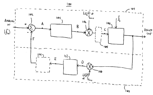
FIG.l shows a preferred embodiment of a frequency translating sigma-
delta (E-D) modulator 100 for converting an analog input signal ("ANALOG IN")
having
an input frequency f.,~ to a digital output signal ("DIGITAL OUT") sampled at
a sampling
frequency f . The E-0 modulator I 00 includes a summing device 102 for adding
the
analog input signal with a feedback analog signal F and for generating a
summer output
signal A representative of the sum of the analog input signal and the feedback
analog
signal. The summer output signal A is filtered by an analog filter 104, which
can be any
frequency selective filter such as a continuous or discrete-time lowpass,
bandpass or
highpass filter. An analog mixer 106 receiving a mixing signal LOa having a
mixer
frequency fe",;x is provided for frequency translating the filtered summer
output signal B
to a frequency translated summer output signal C having one or more frequency
- 10-
CA 02277619 1999-07-16
components, ,e.~., f.,~ t f m~X, different than the input frequency f,.~. As
required, the analog
mixer 106 can be used to translate the frequency spectrum of the filtered
summer output
signal B to higher or lower frequencies within thelfeedforward branch 107 of
the E-D
modulator I 00. The frequency translated summer output signal C is then
converted to the
digital output signal by quantizer I 08, which is coupled to the output of the
analog mixer
106. The quantizer 108 is operated at sampling frequency f and can be any
suitable
Nyquist rate converter, i.e., one-bit comparator or mufti-bit flash converter,
or another E-
D A/D converter. Optionally, the ~-D modulator 100 may also include a second
analog
filter 105, gzg:, a lowpass filter, located between the analog mixer 106 and
the quantizer
108 for filtering undesired frequency components from the frequency translated
summer
output signal.
As shown in FIG. 1, the E-0 modulator 100 further includes a feedback
branch 109 for providing an analog representation of the digital output signal
to the
summing device 102. The feedback branch 109 includes a digital mixer 110
receiving a
mixing signal LOd, i-e., a digital word stream, representing for example a
sine wave
having a second mixer frequency, ff ",;X. The digital mixer 110 takes two
digital sequences,
~,e., the fed-back digital output signal and the local oscillator signal LOd,
and outputs a
signal D whose discrete Fourier transform has a frequency component equal to
the analog
input frequency f". The digital mixer 110 is coupled to the quantizer 108 for
frequency
translating the digital output signal to a frequency translated digital output
signal D,
-11-
CA 02277619 1999-07-16
which is provided to a digital-to-analog converter (DAC) 112 for converting
the
frequency translated digital output signal D to the feedback analog signal F
having a
frequency equal to the input frequency f,.~. Optionally, the feedback branch
109 may also
include an additional fi~ter 114 coupled to the DAC 112 for filtering
undesired signal
f components from the feedback analog signal F.
FIG. 2 shows a block diagram of a E-D modulator 200 similar to the E-D
modulator I 00 of FIG. 1 constructed and arranged as an in-phase/quadrature
("I/Q")
frequency translating E-0 modulator. The I/Q E-D modulator 200 of FIG. 2
includes a
complex analog mixer 206, for frequency translating the individual I/Q
components of the
filtered summer output signal B, and a complex quantizer 208 for sampling the
I/Q
components C, and CQ of the frequency translated summer output signal B at the
sampling frequency fs and for generating I/Q components "I" and "Q" of the
digital
output signal. A complex digital mixer 210 is then provided in the feedback
branch 109
for frequency translating the I/Q components of the digital output signal to a
frequency
1 S translated digital output signal D.
FIG. 3 shows in detail the feedforward and feedback paths 307 and 309,
respectively, of the I/Q ~-D modulator 200 of FIG. 2. FIG. 3 in addition shows
phase
shifters 304 and 310 for creating mixing signals that are 0 degrees and 90
degrees out of
phase corresponding to the in-phase and quadrature phase components,
respectively.
FIG. 4 shows a block diagram of a dual Nyquist rate A/D converter 400
-12-
CA 02277619 1999-07-16
for use as the complex quantizer 208 in the I/Q E-D modulator 200 of FIG. 2.
As shown
in FIG. 4, the A/D converter 400 includes a pair of real A/D converters 402
and 404
corresponding to the individual in-phase and quadrature components C, and CQ,
respectively, of the frequency translated summer output signal. By way of
example and
not limitation, each of the converters 402 and 404 is a one-bit comparator or
a mufti-bit
flash converter for outputting a digital high or low based on a predetermined
voltage
threshold value.
FIG. 5 shows a block diagram of a dual E-D analog-to-digital converter
500 for use as the complex quantizer 208 in the I/Q E-D modulator 200 of FIG.
2. The
converter 500 includes a pair of conventional E-D modulators 501 and 521
corresponding
to the individual in-phase and quadrature components C, and CQ, respectively,
of the
frequency translated summer output signal. Each ~-0 modulator 501 /521
includes a
summer 502/522, an analog filter 504/524, an A/D converter 506/526, and a DAC
508/528 feeding back to the summer 502/522. Preferably, the A/D converters
506/526
are one-bit voltage comparators. Although one-bit comparators are preferred
for
maximum linearity, mufti-bit converters can also be used. In addition, where
the
translated analog signal has two or more frequency components, e_.,g ;, f,." t
f~~X, first-order
I/Q E-D modulators can be used to perform A/D conversion on the low frequency
components only. Optional analog filters 510 and 530 can be provided for
filtering the
DAC 508/528 output for undesired frequency components.
-13-
CA 02277619 1999-07-16
FIG. 6 shows a block diagram of a single ~-0 A/D converter 600 for use
as the complex quantizer 208 in the I/Q E-D modulator 200 of FIG. 2. As shown
in FIG.
6, the E-0 analog-to-digital converter 600 is similar to the converter of FIG.
S, except
that each of the summing devices 602 and 622 include as their inputs both the
fed back
in-phase and quadrature signals. For example, the in-phase summing device 602
includes
as its inputs the analog signal I' from the output of the in-phase A/D
converter 606, and
the analog signal QI' from the output of the quadrature-phase A/D converter
626.
Similarly, the quadrature-phase summer 622 includes as its inputs the analog
signal Q'
and from the output of the quadrature-phase A/D converter 626, and the analog
signal IQ'
from the output of the in-phase A/D converter 606. Each of the analog signals
I', IQ',
QI' and Q' are derived from digital signals I, IQ, QI and Q, respectively, via
DACs 608,
610, 612 and 614, respectively. Each of the DACs 608, 610, 612 and 614 provide
corresponding gains k~, k,Q, lcQ, and 1cQ to the I', IQ', QI' and Q' analog
signals.
FIG. 7 shows a block diagram of a I/Q frequency translating bandpass E-0
modulator 700 utilizing the dual first-order E-D A/D converter 500 of FIG. 5
as the
complex quantizer in the feedforward loop. The I/Q bandpass E-0 modulator 700
uses
direct conversion to baseband within the in-phase and quadrature paths of the
global
feedback loop. The device processes bandpass analog input signals with
continuous-time
circuitry, and I/Q baseband signals with switched-capacitor circuits.
As shown in FIG. 7, the I/Q bandpass E-D modulator 700 includes a
- 14-
CA 02277619 1999-07-16
summing device 702 and an analog filter 704 for filtering the output of the
summing
device 702. Advantageously, the analog filter 704 is a bandpass continuous-
time
resonator, which eliminates the need for front-end S/H circuitry. The analog
filter 704 is
designed to have a low quality factor, or Q, i.e., the ratio of the center
frequency to the 3-
db bandwidth, and as such provides improved performance without significantly
f
impacting resolution of the device when large deviations from the center
frequency are
present.
To obtain high resolution, the A/D converter's gain around the global
feedback loop 750 is kept high at the center frequency for quantization error
attenuation.
The bandpass signal at the resonator output is frequency translated to
baseband by the
analog I/Q mixers 706 and 710, which are coupled to phase shifter 708. The I/Q
signals
are then decimated down, preferably by a factor of two, by decimators 742 and
744 and
processed at baseband by the respective first-order E-D modulators comprised
of the
summing devices 712/714, sampled-data integrators 716/718, A/D converters
720/722,
DACs 724/726 and optional analog filters 728/730. The digital outputs from the
A/D
converters 720 and 722 are then interpolated up by a factor of two by
interpolators 746
and 748, and translated back up to the original center frequency using the
digital I/Q
mixers 732 and 736, which are coupled to phase shifter 734.
Next, the frequency translated in-phase and quadrature digital signals are
combined by summing device 738, and the resulting digital signal is converted
from
-15-
CA 02277619 1999-07-16
digital to analog form using DAC 740. Preferably,~the DAC 740 is a one-bit
DAC. The
converted signal is then fed back to the summing device 702 and subtracted
from the
incoming analog input signal. Local feedback loops, indicated by arrows 751
and 752,
around the baseband first-order sigma-delta modulators are used to stabilize
the system.
Although gain and phase mismatch of the IiQ paths cause image signal
leakage and loss of resolution, the effect of these mismatches is reduced by
the Q of the
analog filter 704 as compared to conventional complex bandpass E-0 modulators.
Seg J.
O. Voorman, U.S. Patent No. 5,157,343, "Electronic Arrangement for Receiving a
Modulated Carrier Signal," issued Oct. 20, 1992; S. Jantzi and K. Martin, "A
Complex
Bandpass Sigma-Delta Converter for Digital Radio," IEEE Custom Integrated
Circuits
Conference, pp. 453-456 (1996). The analog filter 704 of the present
embodiment also
attenuates the effects of mixer non-linearities, particularly third-order non-
linearities.
Translating the spectrum centered at f ~/4 to in-phase and quadrature
signals at baseband is achieved by mixing the resonator output signal with a
local
oscillator having a frequency f m;X = f~/4. The I/Q mixing signals can be, for
example,
sequences (1,0,-1,0...) and (0,1,0; 1...). When the sequence is equal to zero,
there is no
need for the sampled-data integrators 716 and 718 to process the down
converted signals;
hence, the I/Q paths can decimate by a factor of two and operate in a time-
interleaved
fashion. In the feedback path, zeroes are reinserted in both channels in an
interpolation
process and the I/Q signals are added. Alternatively, the DAC 740 can be time
shared by
- 16-
CA 02277619 1999-07-16
both channels rather than directly implementing the summing device 738 of FIG.
7.
Preferably, the DAC 740 is a non-return-to-zero (NRZ), I-bit pulse
shaping DAC and the analog filter 704 is a continuous-time bandpass resonator
having
the fo.lowing transfer function: H(s) = 0.5 * [c~o(wo-s)J/[s-' + c,~~2]. In
the z-domain, as
shown by the block diagram of FIG. 8, the in-phase (p = I) and quadrature (p =
Q) outputs
of the present embodiment can be modeled as:
( I--z 2)( 1 k, i -')NP(z)+k,k3X'p(z)
YF(z) ( 1 )
1 +({k3-I ~k~ ]i 2+(k~k3-k,k3+k,)z-a
where kz = k3 = 0.5, and k2 and k3 control the pole location of the
quantization noise
transfer function. k, represents the effect of the finite Q of the resonator
and is close to
unity. The sigma-delta modulators in the feedforward branch are first-order
sigma-delta
resonators having a sample rate of fs, hence the delays z 2 correspond to i'
at the sample
I 5 rate of f~/2. X'I(z) is the z-transform of the sequence LO[n-2]x[n-4],
where LO[n] is the
local oscillator sequence at the mixers 708 and 734, and is given by the
expression: X',(z)
=-0.5 z~~[X(j z)+X(-j z)]. X'I(z) is X(z) delayed and frequency translated to
baseband.
Similarly, X'Q(z) is the z-transform of the sequence LO[n-3Jx[n-~J and is
given by the
expression: X'Q(z) _ -p.Sj z'~[X(j z)-X( j z)]. NI(z) is the quantization
error of the
in-phase first-order sigma-delta modulator and is modeled as an additive white
noise
sowce. NQ(z) is the quantization error of the quadrature channel.
Forming the output signal, Y(z) = YI(z) + j yQ(z)~ and separating the
- 17-
a
CA 02277619 1999-07-16
transfer functions from the input source X(jz) and the quantization error
sources N,(z) and
NQ(z), the equivalent signal transfer function, STF(z), after frequency
translation to
baseband is:
k,k3 z'~
STF z =
C ) 1 +~(ka_ 1 )-k i ]i z~.(k~k3-k, k3+k, )z'~
Similarly, the noise transfer function NTF(z) is:
(1 z-'-)(1-k, z2)
NTF(z) _ (3)
1+((k~ 1)-k~)iz-~(kzk3 k,k3+kOz-a
NTF(z) corresponds to a second-order conventional baseband sigma-delta with i -
'
replaced by i'. Quantization noise rejection associated with the present
embodiment is
less than a conventional second-order baseband sigma-delta if a finite Q
resonator, i.~., k,
< 1, is used.
The continuous-time resonator of FIG. 7 has been implemented as a
Tow-Thomas active filter having a nominal center frequency of 25 kHz and Q of
10.
Alternatively, other well-known continuous-time active or passive filtering
techniques
can be used. The analog mixers can be realized at the inputs of the first-
order sigma-delta
modulators by controlling the phasing of the sampling switches and using
signal
inversions.
FIG. 9 shows the 2 kHz baseband output spectrum when a 25.5 kHz
-18-
CA 02277619 1999-07-16
sinusoid, with a peak amplitude at 20% of the DAC reference voltage is applied
to a
breadboard prototype operating at a 10 kHz clock frequency. Typical baseband
noise
shaping is shown. The image rejection is 52 dB. FIG. 10 is the simulated
result with. the
same input and a 5% .mixer gain mismatch, which indicates an image 48 dB below
the
desired signal. Both are in good agreement with the calculated value of -20
log,°[0.05/(2Q) ] = 52 dB. This formula is only valid for small
mismatches. To further
verify the image rejection capability of the modulator under large mismatch
conditions,
one of the mixers was given a gain of two while the other one was unity.
Simulation
yields an image rejection ratio of 26 dB while measurement yields 23.3 dB. The
same
quadrature mixer used in an open loop configuration would give an image
rejection of
only 9 dB.
A new bandpass sigma-delta modulator structure has been shown that uses
embedded mixers and performs most of the noise shaping at baseband, with
robust
sampled-data circuitry.
I S The approach utilizes frequency translation inside the feedback loop,
which permits most of the analog signal processing to be performed at baseband
where
circuits can be made robust. Both continuous-time and sample-data circuit
techniques are
used to maximize the center frequency and converter resolution. Use of a low Q
resonator in the feedforward loop attenuates the effect of I/Q mismatches and
mixer non-
linearity in contrast to conventional approaches.
-19-
CA 02277619 1999-07-16
Although the present invention has been described in connection with
particular embodiments thereof, it is to be understood that various
modifications,
alterations and adaptions may be made by those skilled in the art without
departing from
the spirit and scope of the irwention. It is intended that the invention be
limited only by
f the appended claims.
- 20 -