Note: Descriptions are shown in the official language in which they were submitted.
CA 02277717 1999-09-21
AEs, ,3 i,, . w
Title: Circuit and Method for Multiple Match Detection in Content Addressable
Memories
Field of Invention
The present invention generally relates to semiconductor memory devices and
more specifically to detecting multiple matches between search and stored data
in high-
density Content Addressable Memory (CAM) systems.
Background
In many conventional memory systems, such as random access memory, binary
digits (bits) are stored in memory cells, and are accessed by a processor that
specifies a
linear address that is associated with the given cell. This system provides
rapid access to
any portion of the memory system within certain limitations. To facilitate
processor
control, each operation that accesses memory must declare, as a part of the
instruction, the
address of the memory cell/cells required. As the amount of memory increases
the
number of bits per instruction needed to reference a memory cell also
increases. This
diminishes the efficiency of the system. In addition to this drawback,
standard memory
systems are not well designed for a content based search. Content based
searches in
standard memory require a software based algorithmic search under the control
of the
microprocessor. These searches are neither quick nor efficient in using
processor
resources.
To overcome these inadequacies an associative memory system called Content
Addressable Memory (CAM) has been developed. CAM allows cells to be referenced
by
their contents, so it first found use in lookup table implementations such as
cache memory
subsystems and is now rapidly finding use in networking systems. CAM's most
valuable
feature is its ability to perform a search and compare as a single operation.
Specified user
data and stored data can be compared and match and mismatch results can be
returned by
allowing the contents of a comparand register to be compared directly with all
addresses
held in a given memory system's address space simultaneously.
CA 02277717 1999-09-21
In addition to the rows and columns of memory cells, that are common to most
memory systems, CAM also has a matchline and a matchline detection circuit
(DTC). The
DTC is a sense amplifier that senses the changes in the logic state of a
matchline for the
cells in that row. The DTC detects a match or a mismatch during a CAM search
and
compare operation. Though in many early applications it was not a concern,
presently the
detection of multiple matches on a matchline is of great interest.
Distinguishing between a
match and mismatch condition is as simple as declaring a threshold voltage or
current
level between the match and mismatch levels, and determining on which side of
the
threshold the matchline level was. This cannot be done with the presence of
multiple
matches, as the effect that it has is simply to increase the decay rate of the
voltage or
current level.
In a typical CAM system, various memory cells, arranged in a row, are
connected
by a matchline to a detection circuit (DTC). Running orthogonal to the
matchlines are
search lines which carry loaded search data to compare with stored data in the
columns of
CAM cells. Typically, matchlines are precharged to a matchline precharge
voltage, for
example, VDD. If a search result is a match, i.e. search data on the search
line matches
stored data in the CAM cell, then there is no change in the matchline voltage
level, i.e. it
remains at its precharge state, VDD. In the case of a mismatch, a direct
current path is
established between the respective matchline and VSS via the CAM cell and the
voltage
level on that matchline begins to decrease. This voltage drop is then detected
by the
respective DTC. Thus to detect a mismatch, each DTC, associated with each
matchline,
must detect whether a differing voltage level develops as a result of the
search and
compare operation. However, it is advantageous to determine whether a detected
match
has resulted from a single row or from multiple rows.
In order to detect multiple matches, otherwise referred to as hits, the
problem
encountered is one of detecting different voltage levels which can develop on
a line.
United States patent 5,012,448 to Matsuoka et al describes a method for
detecting a
voltage level in a multilevel read only memory (ROM) cell. As shown in Figure
1, the
method and apparatus described therein use a pair of CMOS inverters that are
operated as
small signal amplifiers with an NMOS device used for current sensing. Both
reference
and active side sources are also fed into a current mirror. Though this design
accomplishes the desired task of multilevel sensing, it does so at the cost of
increased heat
2
CA 02277717 1999-09-21
,k x mir
dissipation, and a limited output voltage swing. This increase in heat is a
direct result of
high power consumption by the discrete components and is a limiting factor in
the attempt
to shrink the component size so that it occupies less circuit area.
United States patent 5,446,686 to Bosnyak and Santoro describes a method and
an
apparatus for detecting multiple address matches in a CAM. The described
apparatus, as
shown in Figures 2a, 2b and 2c uses a pair of 'hit' and 'dhit' lines that are
connected to the
power supply terminal (VDD) through a pair of pull-up PMOS transistors. A set
of
NMOS devices NO-N3 on the 'hit' line operate in saturation since the voltages
across the
drain and source terminals are always above a threshold compared to the gate-
to-source
voltage (Vgs) of these devices. The reference transistor has a width to length
ratio that is
1.5 times in dimension relative to any one of the NMOS devices NO-N3 to
provide a 1.5
times saturation current. The reference transistor Nref also operates in its
saturation
region. The Vgs of the Nref device is generated using a rather complex
reference circuit
to ensure appropriate compensation for temperature and voltage
characteristics.
Furthermore, the described apparatus uses a comparator to compare the current
difference
generated on the 'hit' and 'dhit' lines for a single and multiple match
generation. The
comparator is a two-stage area-intensive component that uses bipolar
transistors and
resistors for achieving the desired output.
One limitation of this application is as follows. In order to operate the NMOS
devices NO-N3 and Nref in saturation, the pull-up PMOS devices connecting the
'hit' and
'dhit' lines to the power supply terminal have to have relatively low
resistivity such that
the voltage drop is not significant across them while the devices NO-N3 and
Nref turn on
during sensing. This is required to ensure that the voltage across the drain-
to-source
channel does not change significantly. This is achieved at the cost of
relatively high
current consumption through the 'hit' and 'dhit' lines during the entire
operation, which
presents a limitation for multiple-match detection within high density CAMs.
Furthermore, to operate Nref in saturation, a relatively complex compensating
reference circuit is required to ensure compensation for temperature and
voltage
fluctuations in order to develop a constant reference current. The comparator
itself is area
consuming and consumes constant current. The requirement of bipolar devices
presents a
limitation for use in dynamic random access memories (DRAM), which are
entirely
CMOS based.
3
CA 02277717 1999-09-21
,, ;
In conclusion, the increased demand for large memory systems, and the desire
to
efficiently use these systems for more than simple sequential access requires
a multilevel
sense detector that in an ideal embodiment combines fast sensing with low
power
consumption.
Summary of the Invention
It is an object of this invention to provide a sense amplifier of a relatively
high
efficiency in detecting different voltage levels on a multiple-hit-line of a
content
addressable memory (CAM). It is another object of the invention to achieve
multiple
match detection using a relatively low power and comparatively low circuit
area for
detecting the differences between having multiple hits and non-multiple (zero
or a single)
hit.
Therefore, in accordance with one aspect of the present invention, there is
provided
an apparatus, specifically a signal detection circuit, that comprises a
differential amplifier
having a sense node and a reference node, an activation means for switching
the
differential amplifier between an inactive phase and an active phase, an input
means for
providing the sense node with an input signal permitted to start changing from
a
predetermined precharge level towards a discharge level during said inactive
phase, and a
reference means for providing the reference node with a reference signal that
starts
changing from said precharge level towards a predetermined reference level
during said
inactive phase, whereby the differential amplifier provides a complementary
output
corresponding to the difference between the discharge and the reference levels
when the
difference between the input signal and the reference signal exceeds a
detectable level
during the active phase.
In accordance with one embodiment of the present invention the differential
amplifier comprises a latching circuit for providing the complementary output.
Preferably
the input and reference signals start changing from the precharge level at
approximately
the same time, whereas the active phase begins after a predetermined time
delay from the
time the input and reference signals start changing from the precharge level,
said time
delay being sufficient to permit building up a detectable difference between
the input and
reference signals.
4
CA 02277717 1999-09-21
t,. r ~, ; '~A
The signal detection circuit can be used for detecting a multiplicity of n
match
conditions on a plurality of m matchlines in a high density content
addressable memory,
where 2 <_n<m wherein the input signal is derived from the matchlines. To
achieve this,
the input means is coupled to a plurality of m matchlines, such that the
discharge level is
determined by the number of the match conditions, and the reference level
falls between
discharge level corresponding to n-1 match conditions and that corresponding
to n match
conditions. In a transistor circuit embodiment, the input means comprises a
plurality of
similarly sized m matchline devices connected in parallel to the sense node,
wherein each
matchline device is responsive to a corresponding one of the m matchlines and
the
reference means comprises a reference device and a plurality of m dummy
devices
connected in parallel to the reference node, wherein each dummy device
corresponds to
and has substantially similar electrical characteristics to one of the m
matchline devices,
and wherein the reference device has a size between that of first and second
parallel
combinations of n-1 and n matchline devices respectively. In practical CAM
implementations n=2. The reference device is turned on by an enable signal to
permit a
change in the reference signal from the precharge level, at approximately the
same time as
the matchline devices receive their respective match data. The sense node and
the
reference node are separately coupled to a first power supply terminal through
a pair of
respective clamping devices having substantially similar electrical
characteristics to one
another and a sufficient size for precharging the sense node and the reference
node during
the inactive phase and for preventing the sense node and the reference node
from reaching
a voltage level lower than the threshold voltage of any one of the matchline
devices. The
clamping devices are preferred to have respective sizes suitable for limiting
the current
flow through the matchline devices, the dummy devices and the reference device
substantially below saturation.
Another embodiment of the present invention further comprises a logic circuit
for
turning off the pair of clamping circuits upon the differential amplifier
switching to a
latched state during the active phase. The activation means preferably
comprises a circuit
for enabling the differential amplifier only during the active phase.
In accordance with another aspect of the present invention there is provided
an
apparatus, specifically a signal detection circuit for detecting a
multiplicity of n match
conditions occurring among a plurality of m matchlines within a CAM array
where 25n<
CA 02277717 1999-09-21
~ t
m, comprising a differential amplifier having a sense node for receiving a
time-varying
input signal and a reference node for receiving a time-varying reference
signal, activation
means for switching the differential amplifier between an inactive phase and
an active
phase, precharge means for precharging the sense node and the input node to a
predetermined precharge level, during the inactive phase, input means for
deriving the
input signal from the m matchlines, such that said input signal starts
changing during the
inactive phase from the precharge level to a discharge level determined by the
number of
the match conditions and reference means for generating the reference signal
which starts
changing during the inactive phase from the precharge level towards a
reference level
falling between the discharge levels corresponding to n and n-1 match
conditions
wherein the differential amplifier compares the input signal with the
reference signal
during the active phase and provides a corresponding complementary output that
indicates
whether the number of match conditions is below n or whether it is equal to or
exceeds n.
In accordance with yet another aspect of the present invention there is
provided a
method of detecting a multiplicity of n match conditions occurring among a
plurality of m
matchlines within a CAM array, where 2Sn<m, comprising the steps of providing
a
differential amplifier, turning said differential amplifier into an inactive
state, deriving an
input signal from the m matchlines, such that said input signal starts
changing from a
predetermined precharge level towards a discharge level determined by the
number of the
match conditions, generating a reference signal that starts changing from the
precharge
level towards a reference level falling between the discharge level
corresponding to n
match conditions and that corresponding to n-1 match conditions, and turning
the
differential amplifier into an active state for comparing the input signal
with the reference
signal to obtain an indication whether the number of match conditions is below
n or
whether it is equal to or exceeds n.
The invention avoids the otherwise conventional requirement for operating in
saturation mode the devices driving the multiple hit lines and the reference
line, thereby
minimizing power consumption in the overall circuit.
The differential amplifier detects a difference between voltages on the
multiple-hit
line and the reference line, as opposed to the prior art method of current
detection. Thus
the circuit consumes relatively negligible current without requiring
additional stages for
boosting signal levels to be detected, as in prior art solutions.
6
CA 02277717 1999-09-21
.",
Description of Drawings
Exemplary embodiments of the invention will now be further described with
references to the drawings in which same reference numerals designate similar
parts
throughout the figures thereof, and wherein:
Figure 1 shows a conventional sense amplifier for a multilevel sensing;
Figure 2a, 2b, and 2c show a prior art apparatus for detecting multiple
address
matches in a CAM;
Figure 3 is a schematic diagram illustrating the structure of a multiple-hit-
line to be
sensed and a reference multiple-hit-line; as part of an embodiment of this
invention;
Figure 4 is a schematic diagram illustrating a differential amplifier and
associated
circuits for use with the structure shown in Figure 3, as a first embodiment
of the present
invention; -
Figure 5 is a schematic diagram illustrating a differential application and
associated circuits for use with the structure shown in Figure 3, in a second
embodiment of
the present invention;
Figure 6 is a timing diagram of the multiple match detection operation
performed
by the first embodiment;
Figure 7 is a timing diagram of the multiple match detection operation
performed
by the second embodiment; and
Figures 8a, 8b and 8c are timing diagrams to illustrate the three cases of
multiple,
single and no hit respectively in the second embodiment.
Detailed Description of the Invention
Figure 3 illustrates the structure of a multiple hit line MHL and a reference
line
MHLb as part of one embodiment of the present invention. The multiple hit line
MHL is
coupled to a number (128 in this embodiment) of matchlines ML1-ML128, in
parallel, via
NMOS matchline devices MD1-MD128, which all have similar dimensions and
operating
characteristics. Each of these matchline devices MD1-MD128 is setup so that
its source is
connected to VSS, its drain is connected to MHL, and its gate is connected to
the
7
CA 02277717 1999-09-21
..
respective matchline thereby allowing the voltage level on MHL to be
controlled by the
multiple pull-down paths provided by the matchline devices MD1-MD128. The
number
of matchline devices used in an array of CAM cells is equal to the number of
rows of
CAM cells in that array, which in this embodiment is 128. In turn, each
matchline is
connected to a row of CAM cells, which use the matchline to report the
incidence of a hit
(or a match) and a miss (or a mismatch).
In the above structure, each of the matchlines ML1-ML128 carries match or
mismatch information about the cells in its row. In the event of a mismatch
between
search data and stored data in a CAM cell in a selected row, the corresponding
matchline
is pulled down to VSS (low), from a precharged state of VDD (high) by a
corresponding
matchline sense amplifier (not shown) whereas a match between search and
stored data
will result in that matchline remaining at the precharged VDD level. As long
as at least
one matchline is at the high level, MHL will be discharged towards VSS through
at least
one matchline device. Having more than one matchline reporting a hit (i.e.
remaining at
VDD) results in MHL discharging towards VSS faster. In the event that no
matchline
reports a hit, MHL remains at VDD because all the matchlines are low and none
of the
matchline devices turn on. The purpose of this embodiment is to dintinguish a
multiple hit
condition from a non-multiple hit condition where only one or no match occurs
on MHL.
The second line used by this embodiment is a reference line denoted by MHLb.
This reference line has an equal number (128 in this embodiment) of NMOS dummy
devices DD 1-DD 128 as the number of matchline devices MD 1-MD 128, connected
in a
similar parallel manner, except that the gates are connected to the VSS line
rather than the
actual matchlines ML 1-ML 128, thereby each dummy device simulating a mismatch
condition. These dummy devices DD 1-DD 128 are chosen so as to have electrical
characteristics similar to the matchline devices MD1-MD128 for this purpose,
and thus
provide the same parasitic capacitance and resistive loading on MHLb as is
present on
MHL for noise reduction. As a result, any voltage or temperature variations
will affect
both MHL and MHLb lines equally, and there is no need for a voltage and
temperature
compensation using a reference generator or similar circuits for addressing
this problem.
In addition, there is an NMOS reference device RD on MHLb whose channel width
falls
between one and two times (in this embodiment 3/2) the channel width of any
one of the
matchline devices MD 1-MD 128. The gate of this reference device RD is
connected to a
CA 02277717 1999-09-21
.-
matchline sense enable signal MLSEN which also activates the matchline sense
amplifiers
(not shown) each of which senses and latches relevant matchline data on its
corresponding
matchline. Match data is established on the matchlines ML 1-ML 128 within a
very short
time after MLSEN is driven to VDD. Subsequently, in case of a match, one of
the gates of
the matchline devices MD1-MD128 will be driven to VDD at approximately the
same
time the gate of the reference device RD is driven to VDD by MLSEN. The timing
signal
MLSEN is used to ensure that both MHL and MHLb start to change their voltages
almost
simultaneously. This allows for the current through MHL and MHLb to be
controlled and
limited, as opposed to the prior art solutions, wherein a constant current is
continuously
drawn.
In this first embodiment, MHL and MHLb are both clamped to VDD using two
PMOS voltage clamping devices, shown in Figure 4 as M1 and M2. For a single
hit,
MHL will be pulled down, after a brief settling time, by the matchline that
indicates the hit
to a voltage level slightly higher than MHLb. This is due to the fact that the
matchline
device that indicates the single hit will be on simultaneously with the
clamping device M1
thereby setting up a voltage divider. Since the width of the reference device
RD is 3/2
times the width of any of the matchline devices MD1-MD128, MHLb will be driven
lower
than MHL. In the case of two or more hits (matches), MHL will reach a voltage
level
lower than that of MHLb, after the brief settling time, since the combined
width of the
matchline devices whose gates are at VDD is larger than that of the reference
device RD.
For the case of no matches in the array, the gates of all the matchline
devices MD1-
MD128 are at VSS, thus MHL will stay at the precharged level while MHLb is
driven to a
lower voltage.
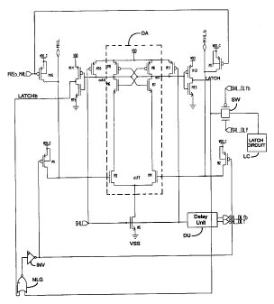
Figure 4 shows a differential amplifier DA and associated circuits used with
the
structure shown in Figure 3 as a first embodiment of this invention. As
indicated above,
the PMOS clamping devices M 1 and M2 are used for clamping MHL and MHLb to
VDD.
The gates of M1 and M2 are connected to VSS making both devices conduct as
soon as
the voltage level on MHL and MHLb drops below VDD-Vtp (the threshold voltage
of a
PMOS device). The source terminals of M1 and M2 are connected to VDD and the
drain
terminal of M1 is connected to MHL while the drain of M2 is connected MHLb.
The
sizes of both M1 and M2 are so chosen as to provide enough current to clamp
MHL and
MLiLb to VDD but M1 and M2 should have such a size as not allow MHL and MHLb
to
9
CA 02277717 1999-09-21
t
reach a voltage level below Vtn, the threshold voltage of NMOS first and
second sensing
devices M3 and M4 used as part of the differential amplifier DA. With this
configuration,
each combination of a PMOS device (M1 or M2) with at least one NMOS device
(MD1-
MD128 or RD, DD1-DD128 respectively) provide a resistive voltage divider that
develops
the respective voltage levels on both MHL and MHLb to be detected by the
differential
amplifier DA. In order to achieve this voltage divider configuration the PMOS
devices are
relatively small thereby reducing the current flow therethrough. The ratio of
transistor
sizes (channel widths) of M1 and any of the matchline devices MD1-MD128 shown
in
Figure 3, determines the voltage level to which MHL will get discharged when a
match
occurs. Similarly, the ratio of transistor sizes of M2 and RD determines the
voltage level
MHLb will reach when RD turns on. These ratios are typically insensitive to
temperature
variations thus eliminating the need for specific measures for temperature
compensation.
A latching circuit of four latch transistor devices M6-M9 together with a pair
of
sensing devices M3 and M4 form the latching differential amplifier DA for
sensing the
level difference developed between MHL and MHLb. An activation circuit that
switches
the differential amplifier DA between an inactive phase and an active phase is
formed by
three activation transistor devices M5, M10, and M11, the gates of which are
connected
together to an activation signal SHL. The inactive phase coincides with SHL
being low
and the MHL and MHLb being precharged to VDD, whereas the active phase
coincides
with SHL being high and MHL and MHLb being sensed. SHL is turned high after
MLSEN is turned high by a specific time delay sufficient to allow the voltage
difference
between MHL and MHLb to reach a level detectable by the differential amplifier
DA.
This is to avoid DA responding to spurious voltages while MHL and MHLb are
discharging towards their respective target levels. It is to be noted that
even during the
active phase, the differential amplifier DA being of a latching type draws
current only
during the switching of the latching circuit M6-M9, and that such switching
occurs rather
rapidly due to the positive feedback connections within the CMOS latching
circuit M6-
M9.
The circuit of Figure 4 also includes an additional conventional output latch
circuit
LC driven by the LATCH signal through a switch SW which is turned on and off
by a
delay unit DU in response to the SHL signal. The delay unit provides two
control signals
SHL- DLY and SHL DLYb which are time delayed versions of SHL. When SHL goes to
CA 02277717 1999-09-21
.. 1 ~~~ v
a low voltage level the path to the latch circuit LC through the switch SW is
disabled,
while a high voltage level MSHL enables the latch circuit.
Figure 6 illustrates the relative timing sequence of the detection operation
performed by the first embodiment combining the circuits of Figures 3 and 4.
During the
inactive phase when SHL is at VSS, first and second output nodes of the
differential
amplifier out and outb respectively, are both precharged to VDD by M10 and Ml
1. SHL
is driven to VDD to switch the differential amplifier DA into the active phase
at the time
when both MHL and MHLb have reached their respective voltage levels as
determined by
the match data on the matchlines ML1-ML12$ which ensure sufficient
differential sensing
margin. After this predetermined delay, SHL goes to VDD and MS turns on with
its gate
driven to VDD. In the case of a multiple hit, MHL settles to a lower voltage
than MHLb,
and the first sensing device M3 being driven by MHL is turned on slightly
while the
second sensing device M4 being driven by MHLb is turned on strongly. This
provides a
higher switching current through M4 and M7 which are connected together in
series, and a
lower current through M3 and M6 which are also connected together in series.
The
resulting differential current in the two paths rapidly switches, i.e. flips
the latching circuit
due to the positive feedback between its four latch transistors M6-M9. As a
result, the
first output node out is driven to VSS while the second output node outb stays
high. Two
pairs of output buffer transistor devices M12, M13 and M14, M15 provide first
and second
inverting buffers BUF l and BUF2 respectively between the first and second
output nodes
out and outb, producing first and second respective output signals LATCH and
LATCHb
to be used in subsequent signal processing. In the case of a single match or
no match,
MHL is at a higher voltage level than MHLb, causing the first sensing
transistor M3 to
turn on harder than the second sensing transistor M4. A differential current
is generated in
an opposite manner as the second output node outb is driven down to VSS while
the first
output node out stays high. The first output node out drives the first
inverting buffer
BUF 1 to provide the first output signal LATCH, which holds the information
for further
processing. It should be noted that the activation signal SHL remains at VDD
only for the
time duration it takes the sensed data to drive the latching circuit M6-M9
(active phase).
Since the first output node out provides the information on multiple hits in a
relatively
short time, current consumption through M 1 and M2 is also for a relatively
short time.
This is clearly shown in Figure 6, which illustrates the timing of a multiple-
hit detection
11
CA 02277717 1999-09-21
'~ , t
operation. As a result, the current flowing through the differential amplifier
DA is only
present during the switching of the latching circuit M6-M9.
Figure 5 shows a differential amplifier and associated circuits used with the
structure shown in Figure 3 as a second embodiment of the present invention
wherein
separate first and second PMOS precharge devices M16 and M17 respectively are
provided in addition to the clamping devices M1 and M2. The differential
amplifier
circuit consisting of M3, M4 and M6-M9 is the same as that shown in Figure 4.
Another
difference between the first and second embodiments is that the pair of
voltage clamping
devices M1 and M2 have their respective gates controlled by the output of an
inverter INV
whose input gate is driven by the output of a NOR logic gate NLG. A first
input of NLG
is connected to the first output signal LATCH provided by the first inverting
buffer BUF 1
formed by the first pair of buffer devices M12 and M13, and a second input of
NLG is
connected to the second output signal LATCHb provided by the second inverting
buffer
BUF2 formed by the second pair of buffer devices M14 and M15. This connection
of the
gates of the voltage clamping devices M 1 and M2 provides self timing to turn
off M 1 and
M2 as soon as the differential amplifier DA has latched the data and switched
from its
precharge state. This provides further reduction in power consumption since M1
and M2
are turned on only for a very limited time during the sensing interval.
Yet another difference from the circuit of the first embodiment shown in
Figure 4
is that instead of using the clamping devices M1 and M2 to precharge MHL and
MHLb,
the precharge devices M16 and M17 are used to precharge the MHL and MHLb lines
using the PREb-MHL signal. Therefore, in this second embodiment as shown in
Figure 5,
the voltage clamping devices M1 and M2 are used only to provide, the logic
levels on
MHL and MHLb and not for precharging as used in the first embodiment. If M1
and M2
were used for precharging as in the first embodiment, the transient current
required for
precharging MHL and MHLb through any PMOS transistor would be larger than the
current needed to develop the voltage levels on these two lines, since in the
second
embodiment, M1 and M2 can be minimum sized transistors. Therefore, if M1 and
M2
were used to perform the precharge, their required larger device sizes would
result in a
larger DC current power dissipation when developing the voltage levels on MHL
and
MHLb during the active phase. In order to address this larger power
dissipation, the
12
CA 02277717 1999-09-21
K
second embodiment of Figure 5 uses the precharge transistors M 16 and M 17 to
perform
the precharge more efficiently.
Figure 7 illustrates the detection operation performed by the second
embodiment
combining the circuits of Figures 3 and 5 in the case of a single hit. As
shown in the
figure, as soon as a difference between MHL and MHLb is detected by the
differential
amplifier DA, both lines begin to be discharged towards VSS by virtue of the
feedback
circuit from the two amplifier outputs out and outb vial the logic gate NLG
and the
inverter INV.
Figures 8a, 8b and 8c illustrate the three possible outcomes of the search and
compare operation on the circuitry described above for the first and second
embodiments
in Figure 6. Figure 8a illustrates the case of a multiple hit where the search
and compare
operation has resulted in more than one hit (or match) between search data and
stored data
in a particular row of the CAM. Note that after a brief period of time, MHL's
voltage
level decreases substantially below that of MHLb, as described earlier, due to
the
combined pull-down action of multiple matchline devices from ML 1-ML 128
(shown in
Figure 3) being turned on simultaneously. These matchline devices
corresponding to the
multiple hits have a combined width which is greater than the width of the
reference
device RD and therefore pull MHL to a voltage level lower than that of MHLb.
Detection
of the voltage difference between MHL and MHLb occurs once the two lines are
sufficiently far apart in voltage to be sensed by the sensing devices M3 and
M4. Shortly
thereafter, the second output node outb obtains a corresponding signal from
the
differential amplifier as described above, MHL and MHLb are both discharged to
VSS,
and then MHL and MHLb are precharged once again in preparation for the next
sensing
operation during the next active phase. Similarly, in Figure 8b, the case of a
single hit is
illustrated. Note that the outcome is opposite to that shown in Figure 8a,
with MHLb
being pulled to a voltage level lower than that of MHL since the single
matchline
transistor that experiences a hit on its associated matchline has a width
which is less than
that of the reference transistor RD. The rest of the sensing operation
proceeds as
described with reference to Figure 8a. Finally, in Figure 8c, the case of no
hits is
illustrated. Here both MHL and MHLb remain at their precharged state since
none of the
matchline devices of Figure 3 are enabled. As can be seen from these three
illustrative
timing charts, the present invention can rapidly distinguish between the three
cases of
13
CA 02277717 1999-09-21
., ~, 1
multiple, single or no hits in a CAM using relatively little power, thereby
permitting the
fabrication of CAM arrays with large cell densities.
Of course, numerous variations and adaptations may be made to the particular
embodiments of the invention described above, without departing from the
spirit and
scope of the invention, which is defined in the claims. Whereas the
embodiments
described above are particularly relevant to high density CAM arrays requiring
detection
of multiple hits, the invention is also applicable to the detection of data
lines having a time
varying voltage level with no pre-set reference.
14