Note: Descriptions are shown in the official language in which they were submitted.
CA 02278161 1999-07-13
- WO 98/34439 PCT/US98/01442
DRIVING CIRCUIT FOR STACKED ORGANIC
LIGHT EMITTING DEVICES
Field Of The Invention
The present invention relates to the field of light
emitting devices, in particular, to stacked organic light
emitting devices (SOLEDs) and to means for driving same.
Background Information
Organic light emitting devices (OLEDs) are light
emitting devices which use organic electrolumi.nescent (EL)
materials excited by electric current to emit light. A plurality
of OLEDs can be arranged :in an array to form a display.
In color disp:la.ys, it is necessary to arrange OLEDs
which emit light of dif:Eerent colors, typically the primary
colors blue, green .and red, in close proximity to each other.
In such an application, it is advantageous to arrange three
OLEDs, each emitting light of one of the three primary colors,
in a stack, thereby forming a true color pixel from which any
color can be emitted. Such a structure is described in PCT
International Application WO 96/19792.
In such a stacked structure, one electrode layer is
provided at the bottom of the SOLED stack and a further electrode
layer is provided between each of the OLEDs in the stack and on
top of the uppermost OLEI) in the stack. The bottom electrode
layer is typically coupled to a ground reference and the
intermediate and top elects rode layers are coupled to either a
positive or negative. driving voltage.
With only one electrode layer being provided in the
SOLED for coupling to a ground reference and with only one
additional electrode: layer being provided for each OLED in the
stack, the problem ~~rises of driving each of the OLEDs in the
stack independently of each other. There is therefore a need for
a means of driving such a configuration of stacked OLEDs or for
1
SUBSTITUTE SHEET (RULE 26)
CA 02278161 1999-07-13
- WO 98/34439 PCT/US98/01442
alternative configurations of stacked OLEDs.
Summary Of The Invention
The present invention is directed to arrangements for
independently driving individual OLEDs arranged in a stacked OLED
structure, or SOLED.
For a conventional SOLED in which only one electrode
is provided between each OLED in the stack and in which only one
electrode, arranged at the bottom of the stack, is coupled to
ground potential, the present invention provides a driving
circuit which generates voltages for application to the
electrodes arranged between the OLEDs in accordance with input
control signals applied to the driving circuit. The brightness
of the light emitted by each OLED of the SOLED is controlled by
the driving circuit in accordance with a respective one of the
input control signals so that there is a direct correspondence
between the level of an input control signal and the brightness
of the light emitted by the corresponding OLED.
The present invention also provides embodiments of
SOLED structures which allow direct control of the individual
OLEDs in the stacked structure with no additional external
circuitry.
In a first such embodiment, each OLED is provided with
a first electrode coupled to a ground reference and a second
electrode coupled to either a positive or negative driving
voltage. An insulating layer is provided between adjacent
electrodes of two of the OLEDs in the stack.
In a further embodiment, each OLED in the stack is
provided with a first electrode for coupling to a ground
reference and a second electrode for coupling to a positive
driving voltage. An insulating layer is provided between
adjacent electrodes of two of the OLEDs in the stack. In
addition, the middle OLED is formed with an inverted structure.
In this embodiment, only driving voltages of the same polarity
are required, thereby avoiding the need for a dual-polarity
voltage source.
In a third embodiment, only one electrode layer is
coupled to ground potential. Each OLED is directly controlled
2
SUBSTITUTE SHEET (RULE 26)
CA 02278161 1999-07-13
- WO 98134439 PCT/US98/01442
and no insulating layers a.re required. The middle OLED is formed
with an inverted structure. Only vcltages of the same polarity
are required.
The circu~_t and SOLEDs of the present invention can be
used in a wide variety of applications, including computer
displays, informational displays in vehicles, television
monitors, telephones, printers, illuminated signs, large-area
screens and billboards.
Brief Descrit~tion O:f The Drawings
Figure 1 ~~hows an exemplary embodiment of a circuit for
driving a conventional stacked OLED structure in accordance with
the present invention.
Figure 2 shows a first embodiment of a stacked OLED
structure in accordance with the present invention.
Figure 3 shows a second embodiment of a stacked OLED
structure in accordance with the present invention.
Figure 4 shows a third embodiment of a stacked OLED
structure in accordance with the present invention.
Detailed Description
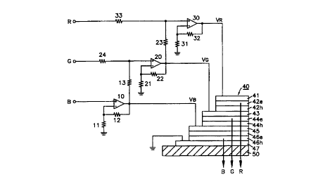
Fig. 1 shows an exemplary embodiment of a circuit for
driving a stacked OLED (SOLED) structure 40. The SOLED structure
of Fig. 1 includes three OLEDs, each emitting one of a red, green
and blue light, represented by arrows labeled R, G and B,
respectively. For the purposes of the present invention, the
actual colors emitted is irrelevant. The primary colors red,
green and blue are preferred in the typical display applications
utilizing SOLEDs so as to allow all possible color combinations.
Furthermore, although a red OLED is shown stacked on a green OLED
which in turn is stacked on a blue OLED, any order of stacking
is possible. The SOLED 40 can be fabricated as disclosed in U.S.
Patent Applications Serial Nos. 08/354,674 and 08/613,207,
incorporated herein by reference in their entirety.
The circuit for driving the OLED stacked structure
includes three driva=rs 10, 20 and 30 which can be implemented,
as shown, with operational amplifiers (op-amps) . Each of the
drivers 10, 20 and 30 has. an input coupled to a terminal, B, G
3
SUBSTITUTE SHEET (RULE 26)
CA 02278161 1999-07-13
- WO 98/34439 PCT/US98/01442
or R, respectively, to which is applied a control signal
indicative of the desired brightness of the light to be emitted
by a corresponding one of the OLEDs in the stacked OLED structure
40.
The stacked OLED structure 40 is fabricated on a
substrate 50 which is composed of a substantially transparent
material such as glass. The bottom layer of the stacked
structure 40 is an electrode layer 47. In the exemplary
embodiment of Fig. 1, the electrode layer 47 acts as an anode and
is coupled to ground. A first OLED which emits blue light is
arranged over the electrode layer 47. The first OLED comprises
a layer 46h of organic material which acts as a hole transporting
layer (HTL). The HTL 46h is deposited on the electrode layer 47.
A further organic layer 46e which acts as an electron
transporting layer (ETL) as well as an electroluminescent layer
(EL) is deposited on the HTL 46h. The ETL and EL can
alternatively be implemented as two distinct layers. A semi-
transparent electrode layer 45 is deposited on the ETL/EL 46e.
A second OLED which emits green light is fabricated
over the first OLED. The second OLED, which is similar in
fabrication to the first OLED, comprises a HTL 44h which is
deposited on the electrode layer 45 and an ETL/EL 44e which is
deposited on the HTL 44h. A semi-transparent electrode layer 43
is deposited on the ETL/EL 44e.
A third OLED which emits red light is fabricated over
the second OLED. The third OLED, which is similar in fabrication
to the first and second OLEDs, comprises a HTL 42h which is
deposited on the electrode layer 43 and an ETL/EL 42e which is
deposited on the HTL 42h. An opaque or semi-transparent
electrode layer 41 is deposited on the ETL/EL 42e.
The electrode 45, which lies between the first and
second OLEDs, is coupled to the output of the driver 10. The
driver 10 generates a voltage VH which drives the first OLED.
The brightness of the blue light emitted by the first OLED is
controlled by the magnitude of the voltage VB.
The electrode 43, which lies between the second and
third OLEDs, is coupled to the output of the driver 20. The
driver 20 generates a voltage V~ which in conjunction with the
4
SUBSTITUTE SHEET (RULE 26)
CA 02278161 1999-07-13
- WO 98/34439 PCT/US98/01442
voltage VB determines the brightness of the green light emitted
by the second OLED. More specifically, the brightness of the
light emitted by th.e second OLED is a function of the voltage
applied across the second OLED. The voltage applied across the
second OLED is the voltage between the electrodes 43 and 45, or
Vc _ VB .
The elect~:ode 41, which lies over the third OLED) is
coupled to the output of the driver 30. The driver 30 generates
a voltage VR which in conjunction with the voltage V~ determines
the brightness of th.e red light emitted by the third OLED. The
brightness of the light emitted by the third OLED is a function
of the voltage applit~d across the third OLED, namely, the voltage
between the electrodes 41 and 43, or VR-V~.
In conjunction with resistors 11 and 12, the op-amp 10
is configured so that the voltage VB generated by the op-amp 10
is equal or proportionate to the voltage of the control signal
applied to the terminal B. The resistor 11 is coupled between
an inverting input of the op-amp 10 and ground and the resistor
12 is coupled between the inverting input and the output of the
op-amp 10. The closed-laop gain of the op-amp l0 thus configured
is determined by the values of the resistors 11 and 12. More
specifically:
Ve = (1 + Rlz/Rii) V (B) ,
where R11 and Rlz are the values of the resistors 11 and 12,
respectively, and V(B) is the voltage of the input control signal
applied to terminal B. 7.f resistor 12 is replaced by a short
circuit, then VA = V(B), i..e., the brightness of the blue OLED is
determined by the voltage applied to the control terminal B.
In conjunction with resistors 13 , 21 , 22 and 24 , the
op-amp 20 can be configured so that the voltage V~ generated by
the op-amp 20 can be made proportionate to the sum of VB and the
voltage applied to the terminal G (V(G)). The terminal G, to
which the control ;signal for the green OLED is applied, is
coupled via the resistor 24 to a non-inverting input of the op-
amp 20. The autput= of the op-amp 10 is coupled to the non-
inverting input of the op-amp 20 via the resistor 13. The
SUBSTITUTE SHEET (RULE 26)
CA 02278161 1999-07-13
- WO 98/34439 PCT/US98/01442
resistor 21 is coupled between an inverting input of the op-amp
20 and ground and the resistor 22 is coupled between the
inverting input and the output of the op-amp 20. In this
configuration, the driver 20 acts as a summing amplifier. If the
values of the resistors 13 and 24 are selected to be equal, then:
V~ _ ~ (1 + Rzz/R2~) [V (G) + VB] .
Furthermore, if the values of the resistors 21 and 22 are
selected to be equal, then V~ - V (G) + V$, in which case the
voltage applied across the green OLED, V~ - VH, is equal to V(G).
In this case, the brightness of the green OLED is controlled only
by the voltage of the signal applied to the terminal G.
The driver 30 is configured with resistors 23, 31, 32
and 33 to operate similarly to driver 20. If the values of
resistors 23 and 33 are selected to be equal to each other and
the values of the resistors 31 and 32 are selected to be equal
to each other, then the voltage applied across the red OLED is
equal to V(R), the voltage of the control signal applied to the
terminal R. In this case, the brightness of the red OLED is
controlled only by the voltage applied to the terminal R.
As a result, the brightness of the light emitted by
each of the OLEDs in the stacked structure 40 can be controlled
independently of the brightness of the other OLEDs, thus
providing a transparent control of the individual OLEDs of the
SOLED from the corresponding input control signals.
It should be noted that if the nominal driving voltage
for an individual OLED in the stacked structure is Vd (typically
approximately 10 volts), the magnitude of the voltage VR applied
to the electrode 41 can be as great as 3Vd (30 volts). As such,
the driver 30 must be capable of developing an output voltage of
3Vd and thus must be powered with a supply voltage of 3Vd or
greater.
Note that in the exemplary embodiment of Fig. l, the
voltages VH, V~ and VR for driving the OLEDs are negative in
polarity. This is due to the ordering of the organic layers of
the individual OLEDs and the grounding of the bottom electrode
47. It should be evident that the circuit of Fig. 1 is also
6
SUBSTITUTE SHEET (RULE 26)
CA 02278161 1999-07-13
- WO 98/34439 PCT/US98/01442
applicable to SOLEDs which require positive driving voltages (as
in the case in which the ETL/EL and HTL of each OLED are
reversed). Moreover, the circuit of Fig. 1 can be readily
adapted to operate with input control signals of either positive
or negative polarit~~.
Fig. 2 shows an embodiment of a stacked OLED structure
60 in which each of the OLEDs in the stack is provided with a
ground reference. 7.n this embodiment, the individual OLEDs in
the stack can be controlled independently of each other without
additional external circuitry such as that of Fig. 1. In this
embodiment, the voltages Vp., V~ and V$ for driving the respective
OLEDs in the SOLED are represented by voltage sources 51, 52 and
53, respectively.
The stacked OLED structure 60 of Fig. 2 is fabricated
on a substantially transparent substrate 70. The first layer
deposited on the sub~~trate 70 is an electrode layer 61 which acts
as the anode for the' blue OLED. The anode layer 61, which can
be composed of indium tin oxide (ITO), receives the voltage VB,
which in this embodiment i:~ positive, for driving the blue OLED.
The organic layers of the blue OLED include an ETL/EL 62e and a
HTL 62h which is dept>sited over the anode layer 61. An electrode
layer 63 is deposited on the ETL/EL 62e. The electrode layer 63,
which can be formed by depositing a thin, semi-transparent layer
of Mg:Ag alloy folloured by a layer of ITO, is connected to ground
potential.
A HTL 64h for the green OLED is deposited over the
electrode layer 63 and an E;TL/EL 64e is deposited on the HTL 64h.
An electrode layer 65, composed of ITO and a thin layer of Mg:Ag
alloy is deposited on th.e HTL 64h. The electrode layer 65
receives the voltage V~, which in this embodiment is negative,
for driving the green OLED and acts as the cathode of the green
OLED. It should be noted that the electrode layer 63, which acts
as the cathode of tine blue OLED also acts as the anode of the
green OLED.
An insulating layer 66 is deposited over the cathode
layer 65. The i.nsula.ting layer can be composed of an insulating
material such a SiC2, SiN X or A10 2deposited by a variety of
processes such as plasma enhanced chemical vapor deposition
7
SUBS'T1TUTE SHEET (RULE 26)
CA 02278161 1999-07-13
- WO 98/34439 PCT/US98/01442
(PECVD), e-beam, etc. An electrode layer 67, which can be
compo~ed of ITO, is deposited over the insulating layer 66. The
electrode layer 67, which acts as the anode of the red OLED, is
connected to ground potential. A HTL 68h of the red OLED is
deposited over the electrode layer 67 and an ETL/EL 68e is
deposited over the HTL 68h. An electrode layer 69 which acts as
the cathode of the red OLED and which can be composed of an Mg:Ag
alloy, is deposited over the ETL/EL 68. The electrode layer 69
receives the voltage VR, which in this embodiment is negative,
for driving the red OLED.
In the embodiment of Fig. 2, the electrode layer 67 is
coupled to ground and the electrode layer 69 is coupled to a
negative voltage. In the alternative, it is also possible to
couple the electrode layer 69 to ground and to couple the
electrode layer 67 to a positive voltage.
Furthermore, in the embodiment of Fig. 2, the order of
deposition of the hole transporting layer and the electron
transporting and electroluminescent layer is the same for all
three of the OLEDs in the stack. Namely, in each case, the
electron transporting and electroluminescent layer is deposited
over the hole transporting layer. It should be evident that a
reverse ordering is also possible, i.e., the hole transporting
layer is deposited over the electron transporting and
electroluminescent layer.
Moreover, in the embodiment of Fig. 2, the insulating
layer 66 is arranged between electrode layers arranged between
the middle and upper OLEDs. The embodiment of Fig. 2, however,
can be readily modified so that the insulating layer is instead
arranged between electrodes arranged between the lower and middle
OLEDs. Fig. 2A shows such an embodiment.
Fig. 3 shows a third embodiment of a stacked OLED
structure 80 in which each of the OLEDs in the stack is provided
with a ground reference. In this embodiment, all of the OLED
driving voltages VR, V~ and VH, provided by the voltages sources
71, 72 and 73, respectively, are of the same polarity. In the
exemplary embodiment of Fig. 3, the polarities of the driving
voltages are positive, although it should be evident that the
SOLED structure can be readily adapted for negative driving
8
SUBSTITUTE SHEET (RULE 26)
CA 02278161 1999-07-13
- WO 98/34439 PCT/US98/01442
voltages.
The stacked OLED structure 80 of Fig. 3 is fabricated
on a substrate 90. The first layer deposited on the substrate
90 is a layer 81 which acts as the anode for the blue OLED. The
anode layer 81, which can be composed of ITO, receives the
voltage VH for driving t:he blue OLED. A HTL 82h for the blue
OLED is deposited over the anode layer 81 and an ETL/EL 82e for
the blue OLED is deposited over the HTL 82h. An electrode layer
83 is deposited on the ET:L/EL 82e. The electrode layer 83, which
can be formed by depositing a thin layer of Mg:Ag alloy followed
by a layer of ITO, is connected to ground potential and acts as
a cathode for the blue OLED.
An ETL/EL~ 84e f:or the green OLED is deposited over the
electrode layer 83 and a HTL 84h is deposited over the ETL/EL
84e. Note that the order of the ETL/EL and HTL of the green OLED
is opposite to that of t:he underlying blue OLED. An electrode
layer 85, which can. be composed of ITO, is deposited on the HTL
84h and acts as the anode for the green OLED. The electrode
layer 85 receives t:he voltage V~ for driving the green OLED. It
should be noted that the electrode layer 83, which acts as the
cathode for the blue OLED also acts as the cathode for the green
OLED.
An insulating layer 86 is deposited over the electrode
layer 85. The insulating layer can be composed of an insulating
material such a S:iOz, SiNX or A102 deposited by a variety of
processes such as P:ECVD, e-beam, etc. A further electrode layer
87 is deposited over the insulating layer 86. The electrode
layer 87, which acts a:a the anode for the red OLED, can be
composed of ITO and is cannected to the voltage VR for driving
the red OLED. A H'TL 88h of the red OLED is deposited over the
electrode layer 87 and an ETL/EL 88e is deposited over the HTL
88h. Note that the order of the HTL and ETL/EL of the red OLED
is the same as that of the blue OLED and the reverse of that of
the green OLED. A cathode layer 89, which can be composed of an
Mg:Ag alloy, is deposited over the ETL/EL 88e. The cathode layer
89 is coupled to ground :potential.
It should be evident that, like the embodiment of Fig.
2, a reverse ordering of the HTL and ETL/EL of each layer is also
9
SUBSTITUTE SHEET (RULE 26)
CA 02278161 1999-07-13
- WO 98/34439 PCT/ITS98/01442
possible with the embodiment of Fig. 3. Moreover, in the
embodiment of Fig. 3, the insulating layer 86 is arranged between
electrode layers arranged between the middle and upper OLEDs .
The embodiment of Fig. 3, however, can be readily modified so
that the insulating layer is instead arranged between electrodes
arranged between the lower and middle OLEDs. Fig. 3A shows such
an embodiment.
Fig. 4 shows yet another exemplary embodiment of a
three-color stacked OLED structure in which only one electrode
is tied to ground potential yet, when all OLEDs are on, does not
require any voltages greater than that needed to drive one OLED
(i.e., Vd).
As shown in Fig. 4, the SOLED is fabricated on a glass
substrate 100. An electrode layer 101 is deposited on the
substrate 100 as a 1500-4000 A thick layer of ITO and acts as the
anode for the first OLED, which in this embodiment emits blue
light. A HTL 102 is deposited on the electrode 101 as a 500 A
thick layer of 4,4'-bis[N-(1-napthyl)-N-phenyl-
amino]biphenyl (a-NPD). An electroluminescent layer 103,
composed of A1q20Ph and having a thickness of I00-1000 P., is
deposited on the HTL 102. An ETL 104 composed of tris-(8-
hydroxyquinoline) aluminum (Alq3) is deposited with a thickness
of 200-800 A on the electroluminescent layer 103. An electrode
layer 105 is deposited on the ETL 104 and acts as the cathode of
the blue OLED. The electrode 105 can be composed of an Mg:Ag
alloy and can have a thickness of 50-200 A. The electrode 105
is connected to ground potential. A voltage VB provided by a
voltage source 91 is applied across the electrodes 101 and 105
to drive the blue OLED.
The structure for the second OLED in the stack, which
in this embodiment is a green light emitting OLED, is fabricated
over the electrode 105. In this embodiment, however, the green
OLED is formed in an inverted configuration. An ETL/EL 106,
composed of Alq3, is deposited on the electrode 105 to a
thickness of 200-800 A. A HTL 107 is deposited as a 100-1000 A
thick layer of NPD on the ETL/EL 106. A protection layer 108 is
deposited on the HTL 107 and an electrode layer 109 composed of
ITO is deposited with a thickness of 300-1000 A on the protection
SUBSTITUTE SHEET (RULE 26)
CA 02278161 1999-07-13
- WO 98/34439 PCT/US98/01442
layer 108. The protection layer 108 can be formed by the
deposition of 3,4,9,10-perylenetetracarboxilic dianhydride
(PTCDA), bis(1,2,5-i=hiadiazolo)-p-quinobis
(1,3-dithiole) (BTQIBT), copper phthalocyanine (CuPc), or other
suitable, more rigid organic materials. The thickness of the
protection layer 108 can preferably be 50-200 A. The electrode
layer 109 acts as the anode for the green OLED and the electrode
layer 105 acts as the cathode. To drive the green OLED, a
voltage V~, provided by a voltage source 92, is applied across
the electrode layers 109 and 105.
The red OLED is fabricated over the ITO electrode layer
109 in an upright configuration. A NPD HTL 110 with a thickness
of 100-1000 A is deposited on the electrode layer 109 and an Alq3
ETL/EL 111 with a thickness of 200-800 A is deposited on the HTL
110. A metallic electrode layer 112, composed for instance of
a 500-2000 A thick layer of Mg:Ag alloy, is arranged on the
ETL/EL 111 and is capped off with a cap layer 113. The cap
layer, which serves 1~o protect the device from oxidation, can be
a 500-2000 A thick layer of silver. The electrode layer 112 acts
as the cathode of the red OLED and the electrode layer 109 acts
as the anode. To drive the red OLED, a voltage VR, provided by
a voltage source 93, is applied across the electrode layers 109
and 112.
In the embodiment of Fig. 4, if the nominal driving
voltage for each of t:he OLEDs in the stack is Vd, when all three
OLEDs are driven ful:L on with the voltage Vd, the voltage V, will
be Vd, V2 will be 0 volts, V3 will be Vd and V4 will be
substantially 0 volts. If, however, the middle (green) OLED is
off while the bottom (blue) and top (red) OLEDs are full on, V1
will be Vd, Vz will be 0 volts, V3 will be substantially 0 volts
and VQ will be substantially -Vd. In this case, the voltage
difference between '~z and V4 will be substantially Vd- (-Vd) or
2Vd. This voltage difference, however, can be substantially
reduced by keeping the voltage across the off OLED (in this case
the green OLED) at tree largest voltage at which the OLED will not
emit light. If the :nominal full-on drive voltage of an OLED is
Vd, the threshold voltage: below which the OLED will not emit
light is approximately .BVd. If the middle (green) OLED is
11
SUBS'TiTUTE SHEET (RULE 26)
CA 02278161 1999-07-13
- WO 98/34439 PCT/US98/01442
driven with a voltage at or slightly below .BVd, so as to keep
the middle OLED off, while the top and bottom OLEDs are driven
with voltages of Vd, then V1 will be Vd, VZ will be 0 volts, V3
will be substantially .BVd and V4 will be substantially .8Vd-Vd,
or -.2Vd. In this case, the voltage difference between V2 and VQ
will be Vd-(-.2Vd) or l.2Vd.
Although the thickness of each layer of the SOLED of
Fig. 4 can be within the preferred ranges of thicknesses
specified above, the specific thicknesses of the various layers
can be advantageously selected to exploit microcavity effects
within the stacked structure. Microcavities between layers can
be established within the stacked structure to provide filtering
of the emitted light. The color of the light emitted by each
OLED can thus be adjusted in accordance with the selection of
layer thicknesses.
Although detailed compositions and thicknesses of the
various layers in a SOLED of the present invention have been
described above in connection with the embodiment of Fig. 4, it
should be evident that said discussion is also applicable to the
other embodiments disclosed herein.
The subject invention as disclosed herein may be used
in conjunction with the subject matter of co-pending application,
"DISPLAYS HAVING MESA PIXEL CONFIGURATION," Attorney Docket No.
10020/9 filed on even date herewith, and being herein
incorporated in its entirety by reference.
The subject invention as disclosed herein may be used
in conjunction with the subject matter of co-pending
applications, "Novel Materials for Multicolor LED's," Attorney
Docket No. 10020/2; "Electron Transporting and Light Emitting
Layers Based on Organic Free Radicals," Attorney docket no.
10020/3; "Multicolor Display Devices," Attorney Docket No.
10020/4; and "Red-Emitting Organic Light Emitting Devices
(LED's)," Attorney Docket No. 10020/5, each of said co-pending
application being filed on December 23, 199&, and being herein
incorporated in its entirety by reference. The subject invention
as disclosed herein may also be used in conjunction with the
subject matter of co-pending application, "Vacuum Deposited, Non-
Polymeric Flexible Organic Light Emitting Devices," Attorney
12
SUBSTITUTE SHEET (RULE 26)
CA 02278161 1999-07-13
- WO 98134439 PCT/US98/01442
Docket No. 10020/8, filed on January 23, 1997, and being herein
incorporated in its entirety by reference. The subject invention
may also be used in conjunction with the subject matter of each
of co-pending U.S. Patent: Applications Serial Nos. 08/354,674,
08/613,207, 08/632,,316, 08/632,322 and 08/693,359 and U.S.
Provisional Patent Applications Serial Nos. 60/010,013 and
60/024,001, each oj= which is also herein incorporated in its
entirety by reference.
13
SU8:3TITUTE SHEET (RULE 26)