Note: Descriptions are shown in the official language in which they were submitted.
CA 02278395 2002-O1-16
1
HIGH-FREQUENCY CIRCUIT DEVICE AND COMMUNICATION APPARATUS
HAVING SPURIOUS MODE PROPAGATION BLOCKING CIRCUIT
BACKGROUND OF THE INVENTION
1. Field of the Invention
Tree present invention relates to a high-
frequency circuit device such a wave guide or a
resonator, havs.ng two parallel planar conductors, and
a communication apparatus employing such a high-
frequency circuit device.
2. Description of the Related Art
A variety of transmission lines may be
employed in .apparatuses operating in the micro-wave
band and the millimeter-wave band. The :Following
transmission lines are typically available: (i) a
grounded copl nar line composed of a dielectric plate
with one side generally coated with a ground
electrode and the other side having a coplanar line
thereon; (ii) a grounded Mot line composed of a
dielectric plate with one side coated with a ground
electrode and the other side having a s:Lot; and (iii)
a planar dielectric line composed of a dielectric
plate with both sides lzav:~ng slots.
Each of the above transmission lines
usually have t:wo parallel planar conductors. When an
electromagnet~.c field :is disturbed by input and
output sections and bend sections of the transmission
line, a spuric>us mode wave (also simply referred to
as a
CA 02278395 1999-07-22
- 2 -
"spurious mode"), such as a parallel-plate mode wave, is
induced and travels between the two parallel planar
conductors. For this reason, the leaky spurious mode
waves interfere with each other between adjacent lines,
presenting the problem of leakage signals.
FIG. 38 illustrates the main transmission mode
of a grounded coplanar line and the distribution of a
parallel-plate mode electromagnetic field which is
generated along with it. As shown, the underside of a
dielectric plate 20 is generally coated with an electrode
21 and the top surface of the dielectric plate 20 has a
strip conductor 19 and an electrode 22. The electrodes
21 and 22 serve as ground electrodes, and the grounded
coplanar line is thus composed of electrodes 21 and 22,
the dielectric plate 20 and the strip conductor 19. In
such a grounded coplanar line, the electromagnetic field
may be disturbed at its edges such that an electric field
is established in a direction perpendicular to the
electrodes 21 and 22, and a parallel-plate mode
electromagnetic field occurs as shown. Solid lines with
arrow heads represent the electric field, broken lines
represent the magnetic field, and two-dot chain lines
represent the distribution of currents.
To control the propagation of such an unwanted
mode wave, through holes are conventionally provided
along both sides of a transmission line at a pitch
shorter than the wavelength of a transmission mode wave,
thereby connecting top and bottom electrodes arranged on
the top and bottom faces of a dielectric plate.
The through holes, arranged along the direction
00910312.W51
CA 02278395 1999-07-22
- 3 -
of propagation for connecting the top and bottom
electrodes, serves as a wall (hereinafter referred to as
a "electric barrier"), blocking the propagation of the
parallel-plate mode wave. However, in a high frequency
region, such as the millimeter-wave band, the dielectric
plate must be thin to control the generation of harmonic
mode waves, and the intervals between the through holes
must be extremely short. This involves high processing
accuracy in the manufacture of the circuit device.
When no through holes are arranged in the
dielectric plate, the dielectric plate having electrodes
thereon are entirely housed in a cutoff wave guide. In
such a case, however, the dimensions of the cutoff wave
guide must be equal to or smaller than half the guide
wavelength, and the dimensional requirements of the wave
guide become severer.
A portion of the electrode where the spurious
mode wave leaks can be partially cut away to form a wall
(hereinafter referred to as a "magnetic wall") to block
the propagation of the spurious mode wave. This
arrangement poses a new problem because the cutout
portion of the electrode functions somewhat as a
resonator.
SU1~ARY OF THE INVENTION
Accordingly, it is an object of the present
invention to provide a high-frequency circuit device
which blocks the propagation of the spurious mode waves
such as parallel-plate mode waves, while being free from
the above-described problem associated with the electric
00410312.W51
CA 02278395 1999-07-22
- 4 -
wall of through holes and the magnetic wall of the cutout
portion of an electrode.
When the electromagnetic field is disturbed on
a strip conductor and electrodes are arranged on both
sides of the strip conductor in a grounded coplanar line,
spurious mode electromagnetic waves, such as a parallel
mode wave, travel between the two parallel electrodes and
reach the boundary of an electrode pattern. Since the
configuration of the transmission line changes beyond the
boundary, a portion of the electromagnetic wave is
reflected from the boundary. The electromagnetic wave is
disturbed at the discontinuity section of the electrode
pattern, as the transmission line, and is converted into
a mode which is transmitted through the transmission line
configuration. Thus, a mode conversion is performed.
The present invention takes advantage of this operation.
A circuit is arranged to reflect a mode into which the
spurious mode such as the parallel-plate mode is
converted, thereby blocking the propagation of the
spurious mode waves beyond the circuit.
A high-frequency circuit device of the present
invention includes at least two planar conductors and a
circuit for exciting an electromagnetic wave between the
two planar conductors. A spurious mode propagation
blocking circuit including a conductor pattern which
blocks the propagation of a spurious mode wave by being
coupled with the spurious mode wave that travels between
the two planar conductors is arranged in at least one of
the two planar conductors. The spurious mode propagation
blocking circuit is coupled with the spurious mode wave
00410312.W51
t J
CA 02278395 1999-07-22
- 5 -
traveling between the two planar conductors, thereby
blocking the propagation of the spurious mode wave.
Since the spurious mode propagation blocking circuit is
formed in the planar conductor by simply patterning the
electrode, any problems, such as the ones associated with
the formation of the through holes in the conventional
art, are not presented.
The conductor pattern of the spurious mode
propagation blocking circuit preferably includes a
plurality of micro-strip lines spaced apart at a pitch
shorter than the wavelength of the electromagnetic wave.
In the high-frequency circuit device of the
present invention, the micro-strip line of the spurious
mode propagation blocking circuit is preferably a serial
connection in which a high-impedance line and a low-
impedance line are alternately connected in series. The
spurious mode, such the parallel-plate mode, is converted
into another mode at the micro-strip line and the
resulting signal at a predetermined frequency is
reflected. The propagation of the spurious mode wave is
thus blocked.
In the high-frequency circuit of the present
invention, a plurality of micro-strip lines are
preferably arranged with their terminals opened. The
spurious mode wave is thus converted into a micro-strip
mode wave, which is then reflected from the open
terminal. The spurious mode wave is thus blocked.
The conductor pattern of the spurious mode
propagation blocking circuit preferably includes a
plurality of basic patterns which are arranged at a pitch
00910312.W51
CA 02278395 1999-07-22
- 6 -
shorter than the wavelength of the electromagnetic wave,
with the line of one basic pattern being connected to the
line of the adjacent basic pattern, and wherein the basic
pattern includes a polygonal or circular electrode for
creating a capacitance with the other planar conductor
different from one planar conductor forming the basic
patterns and a plurality of lines connected to the
electrode. Even when the spurious mode waves are
reflected in a multiple fashion, the circuit device
blocks the spurious mode waves, not only in a direction
perpendicular to the direction of propagation of the
spurious mode wave but also in a direction parallel to or
in an acute (or obtuse) direction with respect to the
direction of propagation of the spurious mode.
Preferably, the electrode which creates a
capacitance with the other planar conductor different
from the one planar conductor forming the basic patterns,
is arranged at a junction position of the adjacent basic
patterns. By choosing a proper circuit constant, a large
blocking capability is provided in the blocking of the
spurious mode wave.
Preferably, from among a plurality of lines
connected to the electrode, no two lines are aligned in a
line with each other in orientation or in junction
position. In this way, the signal from one line (port)
is equally distributed among other lines (ports), thereby
increasing the transmission loss between two ports.
Preferably, the conductor pattern of the
spurious mode propagation blocking circuit includes a
plurality of basic patterns, each pattern being a two-
00910312.W51
CA 02278395 2002-O1-16
terminal pair circuit composed of three strip lines,
one central line and two end lines, connected i.n
series, and wherein the coupling between the end
lines is set to be stronger than the coupling
between the central line and each of the two end
lines. The micro-strip mode wave, into which the
spurious mode is converted, is preferably
sufficiently :reflected(even when a low-dielectric-
constant dielectric plate having an impedance which
does not change greatly with the line width of the
strip line varying, or a thick dielectric plate: is
used) .
Preferably, the circuit for exciting the
electromagnetic wave is a transmission line, and the
spurious mode propagation blocking circuit is
arranged between the transmission line and another
transmission line or a resonator. This arrangement
prevents the interference of leaky waves between the
adjacent transmission lines, and the interference of
leaky waves between the transmission line and t:he
resonator.
Preferably, the transmission line is a
grounded coplanar line, a grounded slot line, a
strip line, a planar dielectric line, or a
dielectric line.
In one embodiment of the present invention
the mircro-strip lines extend in a direction
perpendicular to the grounded coplanar line.
In another embodiment of the present
invention, the micro-strip lines extend in a
direction perpendicular to the grounded slot line.
In :yet another embodiment of the present
CA 02278395 2002-O1-16
7a
invention, t:he micro-strip :Lines extend in a
direction perpendicular to the first and second
dielectric strips.
The circuit for exciting the
electromagnetic wave is preferably a resonator and
the spuriou~~ mode propagation blocking circuit is
preferably arranged ors the periphery of the
resonator. This arrangement prevents the
interference of leaky waves between the resonat:or
and the other transmission line and between one
resonator and the other resonator.
The resonator may be of a type which has
non-conductive cutout portions, formed on parallel
planar
CA 02278395 2002-O1-16
3
conductors and serving as a magnetic. wall. The
electromagnetic wave i.s confined bet:ween the cutout
non-conductive portions. Alr_ernatively, the
resonator may be of a type which has electric walls
formed on parallel planar conductors and the
electromagnetic wave i.s confined between the non-
conductive cutout portions.
A communication apparatus preferably
includes a high-frequency circuit device in a signal
transmission section or in a signal processing
section.
According to an aspect of the present:
invention there is provided a high-frequency circuit
device, comprising:
at: least: two planar conductor disposed
with respect: to one another such that they are
capable of receiving an electromagnetic wave
therebetween; and
a spurious mode propagation blocking
circuit disposed in at. least one of the at lea:~t two
planar conductors, the spurious mode propagation
blocking circuit i.ncludi.ng a conductor pattern
operable to couple with a spurious mode wave,
resulting from the electromagnetic wave, that
propagates between the t.wo planar conductors such
that propagation of the spurious mode wave is
blocked.
Ac:cor_ding to another aspect c>f the present
invention, there i.s provided a high-frequency
circuit device, compri.si.ng:
at least. tow planar conductors disposed
such that they are capable of receiving an
electromagnetic wave t.herebetween; and
CA 02278395 2002-O1-16
8a
a spurious mode propagation blocking
circuit disposed in at: least one of the at least two
planar conductors, the spurious mode propagation
blocking circuit including a conductor pattern
operable to couple with a spurious mode wave,
resulting from the electromagnetic wave, that
propagates between the two planar conductors such
that propagation of_ the spurious mode wave is
blocked,
the conductor pattern of the spuriou~~ mode
propagation blocking circuit including a plura7_ity
of micro-strip lines spaced apart at a pitch which
is shorter than the wavelength of th.e
electromagnetic wave,
adjacent micro-strip lines being
interdigital.ly disposed and extending in directions
transverse to the direction of propagation of t:he
electromagnetic wave, and
each micro-strip line including a terminal
end which is open c:ircu.ited.
According to yet another aspect there is
provided a high-frequency circuit device,
comprising:
a dielectric plate having spaced apart
opposing surfaces;
first and second conductors, one conductor
being disposed on each opposing surface of the
dielectric plate such that they are capable of
receiving an e:l.ectromagnetic wave therebetween;
a substantially circular non-conductive
portion loca.twd in the first conductor to produce a
resonator; and
a swpurious mode propagation blocking
circuit disposed in the first conductor and
CA 02278395 2002-O1-16
8b
including a conductor pattern operable to couple
with a spurious mode wave, resulting from
electromagetic wave, that propagates between the two
planar conductors such that propagation, of the
spurious mode wave is blocked,
the conductor pattern of the spurious mode
propagation blocking circuit including a plurality
of micro-strip lines spaced apart at a pitch which
is shorter than the wavelength of the
electromagnetic wave.
According tc> a further aspect of the
present invention, there is provided a high-
frequency device, comprising:
a dielectric plate having spaced apart
opposing surfaces;
first and second conductors, one conductor
disposed on each opposing surface of the dielectric
plate such that they are capable of receiving an
electromagnetic wave therebetween;
a spurious mode propagation blocking
circuit disposed in the first conductor, the
spurious mode propagation blocking circuit including
a conductor pattern operable to couple with a
spurious mode wave, resulting from t:he
electromagnetic wave, that propagates between t;he
two planar conductors such that propagation of the
spurious mode wave is blocked,
the conductc>r pattern of the spuriou:~ mode
propagation blocking ci.rcui.t comprising plurality of
micro-strip lines spaced apart at a pitch which is
shorter than the wavelength of the electromagnetic
wave,
each micro-strip line in the conductor
pattern including (ii a central conductive portion
CA 02278395 2002-O1-16
8c
forming a capacitor with the second conductor on the
opposite surface of the dielectric block, the
central portion having a peripheral edge; and (ii) a
plurality of conductive lines extending from the
peripheral edge of the central conductive portion to
form respective inductances, sets of conductive
lines from adjacent micro-strip lines being
connected together.
BRIEF DESCRIPTION OF THE DRAWINGS
FIG. 1A is a top view showing a high--
frequency circuit device of a first embodiment of the
present invention, and FIG. 1.B is a cross-sectional view
of the high-frequency c.ircui.t.;
FIG. 2 is an equivalent circuit diagram of
the high-frequency circuit of: FIG. 1A having a
transmission line and a spurious mode propagation
blocking circuit;
FI:G. 3 i.s a perspective view showing a
mode converting section between a wave guide mode and a
micro-strip mode;
FIG. 4 shows characteristics of the mode
converting section;
FIGS. 5A and 5B are equivalent circuit
diagrams of the spurious mode propagation blocking
circuit;
FIG. 6 is a characteristic diagram of. the
spurious mode propagation blocking circuit;
FIGS. 7A and 7B show modes ir_ the spurious
mode propagation block circuit;
FIGS. 8A and 8B show how the spuriou:~ mode
CA 02278395 1999-07-22
_ g _
propagation blocking circuit is driven by a parallel-
plate mode wave;
FIGS. 9A and 9B are perspective views of an
evaluation device of the spurious mode propagation
blocking circuit;
FIG. 10 is a top view of the circuit of the
evaluation device;
FIGS. 11A and 11B are characteristic diagrams
of the circuit of the evaluation device shown in FIGS. 9A
and 9B;
FIGS. 12A and 12B show a grounded coplanar line
associated with a spurious mode propagation blocking
circuit;
FIG. 13 shows a grounded slot line associated
with a spurious mode propagation blocking circuit;
FIGS. 14A and 14B show another grounded slot
line associated with a spurious mode propagation blocking
circuit;
FIGS. 15A and 15B show a planar dielectric line
associated with a spurious mode propagation blocking
circuit;
FIGS. 16A and 16B show a dielectric line
associated with a spurious mode propagation blocking
circuit;
FIG. 17 is a top view showing another spurious
mode propagation blocking circuit;
FIG. 18 shows a high-frequency circuit device
having a resonator, associated with a spurious mode
propagation blocking circuit;
FIG. 19 shows another high-frequency circuit
00910312.W51
CA 02278395 1999-07-22
- 10 -
device having a resonator, associated with a spurious
mode propagation blocking circuit;
FIG. 20 shows yet another high-frequency
circuit device having a resonator, associated with a
spurious mode propagation blocking circuit;
FIG. 21 shows the construction of a voltage-
controlled oscillator;
FIG. 22 shows the construction of a
communication apparatus;
FIGS. 23A, 23B and 23C show basic circuit
arrangements of the spurious mode propagation blocking
circuit;
FIG. 24 shows electrical characteristics of the
circuit shown in FIG. 23C;
FIGS. 25A and 25B show a two-dimensional
arrangement of the basic circuit shown in FIG. 23C;
FIG. 26 shows electrical characteristics of the
circuit shown in FIGS. 25A and 25B;
FIG. 27 shows a basic circuit of the spurious
mode propagation blocking circuit;
FIGS. 28A and 28B show a two-dimensional
arrangement of the basic circuit shown in FIG. 27;
FIG. 29 shows electrical characteristics of the
circuit shown in FIGS. 28A and 28B;
FIGS. 30A through 30D show the basic circuit
shown in FIG. 28A and its modification;
FIGS. 31A and 31B show electrical
characteristics of the circuit shown in FIG. 30C;
FIGS. 32A and 32B show electrical
characteristics of the circuit shown in FIG. 30D;
00910312.W51
CA 02278395 1999-07-22
- 11 -
FIGS. 33A and 33B show a high-frequency module
having a spurious mode propagation blocking circuit;
FIG. 34 shows a basic circuit of the spurious
mode propagation blocking circuit;
FIGS. 35A and 35B show a two-dimensional
arrangement of the basic circuit shown in FIG. 34;
FIGS. 36A and 36B show a basic pattern of the
spurious mode propagation blocking circuit;
FIG. 37 shows electrical characteristics of the
circuit shown in FIG. 36; and
FIG. 38 is a perspective view of a parallel-
plate mode wave in a grounded coplanar line with a
portion broken away.
DESCRIPTION OF THE PREFERRED EI~ODII~NTS
The embodiments of a high-frequency circuit
device of the present invention are now discussed,
referring to FIG. 1A through FIG. 11B.
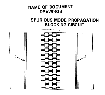
FIG. 1A is a top view showing a major portion
of the high-frequency circuit device. Referring to FIG.
1A, coplanar lines 1 and 2 run parallel to each other on
the top surface of a dielectric plate, and a spurious
mode propagation blocking circuit 3, centrally running
between the two lines 1 and 2, are formed by patterning
an electrode on the top surface of the dielectric plate.
FIG. 1B is an enlarged view showing a portion of the
spurious mode propagation blocking circuit 3.
In such a grounded coplanar line, a spurious
mode wave, such as a parallel-plate mode wave, travels
between top and bottom electrodes of the dielectric
00910312.W51
CA 02278395 1999-07-22
- 12 -
plate, and is then converted into a variety of modes by
the spurious mode propagation blocking circuit 3 under a
disturbance in the electromagnetic field between the
central strip conductors and the electrodes on both
sides. FIG. 2 is an equivalent circuit diagram of the
grounded coplanar line. A parallel-plate mode wave is
induced at a discontinuity section of the grounded
coplanar line, and is then converted, by the spurious
mode propagation blocking circuit 3, into a variety of
modes including a TE010 mode, a slot mode and a micro-
strip mode.
One of the mode waves traveling along the
spurious mode propagation blocking circuit 3 is a quasi
TEM mode of the micro strip. The amount of mode
conversion at a boundary is discussed before discussing
the mode conversion from the parallel-plate mode by the
spurious mode propagation blocking circuit 3 shown in
FIG. 1.
FIG. 3 is a perspective view showing the
construction of a line converter, between a TE10 wave
guide and a micro-strip line, to be used for calculation.
Since the TE10 wave guide mode is equivalent to the
parallel-plate mode in mode configuration, the TE10 mode
wave guide is treated here as a transmission line of
parallel-plate mode. Here, the width W1 of the wave
guide is 3.4 mm (half the wavelength of the wave along
the micro strip), the thickness t of the dielectric plate
is 0.3 mm, the specific dielectric constant r of the
dielectric plate is 3.2, the width W2 of the micro strip
is 0.72 mm, and the characteristic impedance of the micro
00910312.W51
CA 02278395 1999-07-22
- 13 -
strip line is 50 S2.
FIG. 4 shows an input reflection coefficient
S11 and a forward transmission coefficient 521, versus
frequency, of the line converter between the TE10 wave
guide and the micro-strip line, determined using a three-
dimensional electromagnetic field analysis simulator. At
30 GHz, as shown, the forward transmission coefficient
S21 is -1.5 dB or lower, and the input reflection
coefficient S11 is as low as -15 dB. An incident TE wave
is mostly converted into the quasi TEM mode wave of the
micro strip without being reflected.
Since the quasi TEM mode wave in the micro
strip has no cutoff frequency, it can be a transmission
mode wave against any frequency. As shown in FIG. 1B, a
pattern is created so that the wave is fully reflected at
a desired frequency (here, 30 GHz). Referring to FIG.
1B, Wa=0.3 mm, Wb=1.5 mm, Ws=1.5 mm, and the thickness of
the dielectric plate is 0.3 mm. The portion of the line
having a line width Wb corresponds to a low-impedance
line, and the portion of the line having a line width Wa
corresponds to a high-impedance line. One micro-strip
line of the spurious mode propagation blocking circuit 3
is equivalently a circuit composed of two different
characteristic impedances alternately connected in
series, each having its constant electrical length.
FIGS. 5A and 5B show such equivalent circuits. FIG. 5A
shows the equivalent circuit that starts with a high-
impedance line and ends with a high-impedance line. FIG.
5B shows the equivalent circuit that starts with a low-
impedance line and ends with a low-impedance line (here,
00910312.W51
CA 02278395 1999-07-22
- 14 -
Za>Zb). Referring to FIG. 1B, Ws is 1.5 mm, and is one-
quarter of the wavelength along the micro-strip line
(i.e., 30 GHz). Electrical lengths 8a and 8b in the
equivalent circuit are respectively ~/2.
With each micro-strip line thus constructed,
the signal having a desired frequency is fully reflected
as shown in FIG. 6.
When a plurality of micro-strip lines are
arranged, the pitch Wp of adjacent micro-strip lines is
sufficiently shorter than the wavelength of the parallel-
plate mode wave. In this embodiment, Wp=1.5 mm. For
this reason, the parallel-plate mode does not leak out of
the micro-strip lines.
The spurious mode propagation blocking circuit
3 thus includes the micro-strip line composed of high-
impedance lines and low-impedance lines, alternately
connected in series, each having a constant electrical
length. The spurious mode propagation blocking circuit 3
fully reflects the signal having a predetermined
frequency. In the spurious mode propagation blocking
circuit 3, a TE mode wave and a slot mode wave can be
transmitted, besides the quasi TEM mode wave as the
micro-strip mode wave. FIG. 7A shows a TE01 mode and
FIG. 7B shows a slot mode.
The TE mode is now discussed. Referring to
FIG. 7A, a solid line represents the electric field, a
broken line represents the magnetic field, and a two-dot
chain line represents the distribution of currents. In
the TE mode configuration, the electric field is
perpendicular to the parallel planar conductor while the
00410312.W51
CA 02278395 1999-07-22
- 15 -
magnetic field is looped parallel to the surface of an
electrode.
FIGS. 8A and 8B show the electromagnetic field
on the boundary of the spurious mode propagation blocking
circuit 3. FIG. 8A is a perspective view of the
boundary, and FIG. 8B is a cross-sectional view of the
boundary. As shown, the dotted line represents the
magnetic field and the two-dot chain line represents the
distribution of currents. Since adjacent lines, each
having the high-impedance lines and the low-impedance
lines, alternately connected in series, are driven by the
same phase currents, a center surface between the two
adjacent lines is considered to be an electric wall. The
spurious mode propagation blocking circuit 3 is thus
approximated to be a wave guide having a metal wall
covering the boundary between the two adjacent lines. In
this embodiment, there is a possibility that a square
electrode, as large as 1.5 mm by 1.5 mm, functions as a
TE110 mode resonator. The resonance frequency of the
TE110 mode resonator is determined by calculation to be
79 GHz in this case. The cutoff frequency of the wave
guide, rather than the resonator, is 58 GHz, and is
sufficiently higher than the desired frequency (i.e., 30
GHz). The TE mode becomes therefore a non-transmission
mode.
The propagation of the slot mode is now
considered. Referring to FIG. 7B, the spurious mode
propagation blocking circuit has a slot between two
adjacent lines. Since a disturbance taking place on the
boundary of the spurious mode propagation blocking
00410312.W51
CA 02278395 1999-07-22
- 16 -
circuit 3 excites two adjacent lines at the same phase,
as shown in FIGS. 8A and 8B, no slot mode is generated,
in principle.
The electromagnetic wave modes transmitting the
spurious mode propagation blocking circuit are only the
quasi TEM mode of the micro-strip line. If a pattern is
designed to fully reflect this mode, the propagation of
the parallel-plate mode is thus prevented.
Evaluation circuit patterns are shown in FIG.
9A through FIG. 10. FIG. 9A shows an evaluation circuit
having a spurious mode propagation blocking circuit
formed thereon and FIG. 9B shows an evaluation circuit
having no spurious mode propagation blocking circuit.
FIG. 10 is a top view of the evaluation circuit shown in
FIG. 9A. Referring to FIG. 9A, a grounded coplanar line
includes micro-strip lines 11 and 12, respectively, as
input and output lines, an electrode 22 formed alongside
them, and an electrode 21 formed on the underside of a
dielectric plate 20. Unlike a regular grounded coplanar
line, one side portion of the electrode is removed to
destroy bilateral symmetry and to promote the generation
of the parallel-plate mode wave. The output and input
patterns have identical configurations to pick up the
parallel-plate mode. This is based on the reciprocity
theorem derived from Green's theorem, applied to the
circuit.
Referring to FIG. 10, the separation between
each of the micro-strip conductors 11 and 12 and the
electrode 22 is as short as 0.1 mm. This electrode
pattern disturbs the electromagnetic field in the maim
00410312.W51
CA 02278395 1999-07-22
- 17 -
transmission mode (i.e., TEM mode) traveling along the
path, thereby converting it into a parallel-plate mode
wave. The parallel-plate mode wave thus travels between
the top and bottom electrodes 21 and 22 of the dielectric
plate. This works in the same manner as the propagation
of a radiation mode wave in a leaky wave antenna.
FIGS. 11A and 11B show the forward transmission
coefficients S21 of the two evaluation circuits,
respectively shown in FIGS. 9A and 9B. Without the
spurious mode propagation blocking circuit 3, the
parallel-plate mode wave travels at a level of -2 to -3
dB or higher in a range of 25 to 35 GHz. In contrast,
the evaluation circuit with the spurious mode propagation
blocking circuit 3 attenuates the parallel-plate mode
wave to a level of -30 dB or lower in a range of 25 to 35
GHz.
Referring to FIG. 12A through FIG. 16B,
specific examples of high-frequency circuit devices are
discussed.
FIG. 12A is a perspective view of one example
of a high-frequency circuit device and FIG. 12B is an
enlarged underside view of the same high-frequency
circuit device. As shown, an electrode 21 is formed on
the bottom surface of a dielectric plate 20, and an
electrode 22 and a strip conductor 19 are formed on the
top surface of the dielectric plate 20. The strip
conductor 19 partly functions as a grounded coplanar line
1. By patterning the electrode 21 on the underside of
the dielectric plate 20, the spurious mode propagation
blocking circuits 3 are formed on both sides of the
00910312.W51
CA 02278395 1999-07-22
- 18 -
grounded coplanar line 1. The spurious mode propagation
blocking circuit 3 may be formed not only on the surface
of the strip conductor 19 but also on the underside of
the dielectric plate 20, and the parallel-plate mode wave
traveling between the electrodes 21 and 22 is converted
into the quasi TEM mode of the micro strip of the
spurious mode propagation blocking circuit 3, and is then
fully reflected. In this way, almost no parallel-plate
mode travels beyond the spurious mode propagation
blocking circuit 3.
In a high-frequency circuit device shown in
FIG. 13, an electrode 21 is formed on the entire bottom
surface of a dielectric plate 20. Electrodes 22 are
formed on the top surface of the dielectric plate 20. A
slot is arranged in a predetermined position, forming a
grounded slot line 4. By patterning the electrodes 22,
spurious mode propagation blocking circuits 3 are formed
on both sides of the slot.
In contrast to the high-frequency circuit
device shown in FIG. 13, a high-frequency circuit device
shown in FIGS. 14A and 14B includes an electrode 21
formed on the underside of a dielectric plate 20 and
electrodes 22 and a grounded slot line 4 formed on the
top surface of the dielectric plate 20. The electrode 21
on the underside of the dielectric plate 20 is patterned
to form spurious mode propagation blocking circuits 3 on
areas corresponding to both sides of the line on the
surf ace .
With the grounded slot line thus constructed,
the propagation of the parallel-plate mode is equally
00410312.W51
CA 02278395 1999-07-22
- 19 -
blocked.
FIGS. 15A and 15B show a high-frequency circuit
device employing a planar dielectric transmission line
(PDTL). FIG. 15A is a perspective view of the device,
and FIG. 15B is an underside view of its dielectric plate
20. The dielectric plate 20 is interposed between
opposing electrodes 23 and 24, each having a slot. The
dielectric plate 20 and the electrodes 23 and 24 are then
interposed between conductive plates 27 and 28 which
remain parallel to each other with a predetermined space
maintained therebetween. A patent application for the
planar dielectric transmission line thus constructed has
been filed in the Japanese Patent Office (Japanese
Unexamined Patent Publication No. 7-69867).
Spurious mode propagation blocking circuits 3,
the same as those shown in FIG. 1, are formed on both
sides of a slot 26, by patterning the top electrodes 24
on the dielectric plate 20.
With this arrangement, the parallel-plate mode
traveling between the top and bottom electrodes 23 and 24
of the dielectric plate 20, the parallel-plate mode
traveling in a space between the electrodes 24 and the
conductive plate 28 and the parallel-plate mode traveling
in a space between the electrodes 23 and the conductive
plate 27 are all converted into the quasi TEM mode of the
micro strip of the spurious mode propagation blocking
circuits 3, and are then fully reflected. In this way,
the propagation of the spurious mode is blocked.
FIGS. 16A and 16B show a high-frequency circuit
device having a dielectric transmission line in which the
00910312.w51
CA 02278395 1999-07-22
- 20 -
present invention is implemented. FIG. 16A is a
perspective view of the device with a portion broken away
to reveal the inside of the device. FIG. 16B is a cross-
sectional view of the device. Arranged between
conductive plates 31 and 32 are dielectric strips 35 and
36 and a dielectric plate 33 having an electrode 34 on
its top surface. A nonradiative dielectric guide (NRD
guide) thus constructed confines the energy of
electromagnetic field to the dielectric strips 35 and 36,
thereby permitting the electromagnetic wave to travel
therethrough.
The dielectric transmission line generally
disturbs the electromagnetic field at its discontinuity
section such as a splice of dielectric strips or a bend,
permitting the spurious mode, such as the parallel-plate
mode, to travel between the top and bottom conductors.
Spurious mode propagation blocking circuits 3
are arranged on both sides of the dielectric strips 35
and 36, by patterning the electrodes 34 on the top
surface of the dielectric plate 33. The electromagnetic
waves in the parallel-plate mode respectively traveling
in a space A1 between the electrodes 34 and the top
conductive plate 32 and in a space A2 between the
electrodes 34 and the bottom conductive plate 31 are
converted into the quasi TEM mode waves through the
micro-strip lines of the spurious mode propagation
blocking circuits 3, and are then reflected. Leaky waves
between this dielectric transmission line and another
adjacent transmission line of dielectric strips are
prevented from interfering with each other.
00910312.W51
CA 02278395 1999-07-22
- 21 -
A spurious mode propagation blocking circuit 3
of another embodiment is shown in FIG. 17. In this
embodiment, the circuit includes a plurality of micro
strip lines, each having an open terminal, arranged in
parallel. In this embodiment, micro-strip lines 17
extending rightward and micro-strip lines 18 extending
leftward are arranged in an interdigital fashion.
Transmission lines (not shown), such as grounded coplanar
lines, vertically run along both sides of the spurious
mode propagation blocking circuit 3 in FIG. 17. This
arrangement blocks the propagation of the spurious mode
wave in a direction (as represented by arrows)
perpendicular to the direction of propagation of the
electromagnetic wave along the lines.
The pitch Wp of the adjacent micro-strip lines
is substantially shorter than the wavelength of the
parallel-plate mode wave. Such a short pitch of Wp
prevents the parallel-plate mode wave from leaking
between the micro-strip lines. The length Ws of each
micro-strip line is set to be shorter than half the
wavelength of a desired frequency (i.e., a frequency of
the slot mode wave induced between the adjacent micro-
strip lines). With this arrangement, the cutoff
frequency of the slot mode is made sufficiently high, and
the spurious mode, such as the parallel-plate mode, is
not converted into the slot mode. No slot mode is thus
converted back into a parallel-plate mode, resulting no
traveling parallel-plate mode.
The electromagnetic wave in the spurious mode,
such as the parallel-plate mode, traveling between
00910312.W51
CA 02278395 1999-07-22
- 22 -
electrodes on the top surface and the bottom surface of
the dielectric plate, is converted into the quasi TEM
mode on the micro-strip line section. Since the micro-
strip line is opened at its terminal, the quasi TEM mode
wave is fully reflected there. As a result, almost no
spurious mode, such as the parallel-plate mode, travels
beyond the spurious mode propagation blocking circuits 3.
In the device shown in FIG. 17, including the micro-strip
lines 17 extending rightward and the micro-strips lines
18 extending leftward, the parallel-plate mode traveling
rightward is blocked by the micro-strip lines 17 and the
parallel-plate mode traveling leftward is blocked by the
micro-strip lines 18.
Referring to FIG. 18 through FIG. 20, high-
frequency circuit devices having a resonator are
discussed.
In the high-frequency circuit device shown in
FIG. 18, a dielectric plate 29 has one electrode on its
top surface and the other electrode on its bottom
surface. The two electrodes have respective circular
non-conductive portions facing each other. Designated 30
is the circular non-conductive portion arranged on the
top electrode. With this arrangement, a resonator, a
TE010 mode resonator in this example, is formed with the
non-conductive portions working as an electric wall. A
spurious mode propagation blocking circuit 3 is patterned
on the top electrode of the dielectric plate 29. The
spurious mode propagation blocking circuit 3 is
constructed by radially arranging, around the resonator,
micro-strip lines, each including high-impedance lines
00410312.W51
CA 02278395 1999-07-22
- 23 -
and low-impedance lines alternately connected in series
as shown in FIG. 1A. The pattern of the spurious mode
propagation blocking circuit 3 shown in FIG. 18
corresponds to a pattern, expressed in the polar
coordinate system, into which the pattern of the spurious
mode propagation blocking circuit 3 shown in FIG. 1A,
expressed in the Cartesian coordinate system is
converted. Optionally, the wide line width and the
narrow line width may be consistently set in dimension
along the same micro-strip line. FIG. 18 shows only part
of the spurious mode propagation blocking circuit 3.
Some of the energy of the electromagnetic field
confined to the dielectric resonator radially spreads in
the parallel-plate mode between the top and bottom
electrodes on the dielectric plate 29 from the dielectric
resonator. The parallel-plate mode wave is then
converted into the quasi TEM mode wave and fully
reflected by the spurious mode propagation blocking
circuit 3. For this reason, almost no spurious mode
leaks out of the spurious mode propagation blocking
circuit 3. Conversely, almost no spurious mode wave
leaks into the spurious mode propagation blocking circuit
3 (toward the resonator). Even if transmission lines or
other resonators are present outside the spurious mode
propagation blocking circuit 3, no interference takes
place between leaky waves.
FIG. 19 shows the high-frequency circuit device
shown in FIG. 18, with its spurious mode propagation
blocking circuit 3 replaced with another spurious mode
propagation blocking circuit. The spurious mode
00910312.W51
CA 02278395 1999-07-22
- 24 -
propagation blocking circuit 3 here is constructed by
radially arranging, around a resonator, a plurality of
micro-strip lines, each having an open terminal. FIG. 19
shows only part of the spurious mode propagation blocking
circuit 3. The pattern of the spurious mode propagation
blocking circuit 3 shown in FIG. 19 corresponds to a
pattern, expressed in the polar coordinate system, into
which the pattern of the spurious mode propagation
blocking circuit 3 shown in FIG. 17, expressed in the
Cartesian coordinate system is converted. The width of
each micro strip line is fixed.
Referring to FIG. 20, an electrode is formed on
the entire bottom surface of a dielectric plate 29, and a
circular resonator electrode 37 is formed on the top
surface of the dielectric plate 29. The arrangement
results in a planar circuit resonator. The resonator
functions as a TMO11 mode dielectric resonator with the
resonator electrode 37 as an electric wall. A spurious
mode propagation blocking circuit 3 is also patterned on
the top electrode of the dielectric plate 29.
A spurious mode propagation blocking circuit 3
can be formed on the bottom electrode entirely covering
the underside of the dielectric plate 29. In the same
manner as in FIG. 19, the spurious mode propagation
blocking circuit 3 here can be constructed by radially
arranging, around a resonator, a plurality of micro-strip
lines, each having an open terminal.
A voltage-controlled oscillator is now
discussed, referring to FIG. 21 and FIG. 22.
FIG. 21 is a perspective view showing the
00910312.W51
CA 02278395 1999-07-22
- 25 -
construction of the voltage-controlled oscillator. A
dielectric plate 20 is interposed between top and bottom
conductive plates 41 and 44 (the top conductive plate 41
is shown spaced apart from the dielectric plate 20 in
FIG. 21). The dielectric plate 20 has conductive
patterns on its top and bottom surfaces. A slot
transmission line input field-effect transistor
(millimeter-wave GaAs FET) 50 is mounted on the top
surface of the dielectric plate 20. Each of slots 62 and
63, formed on the top surface of the dielectric plate 20,
maintains a fixed space between two respective
electrodes, and constitute a planar dielectric
transmission line along with slots on the underside of
the dielectric plate 20. Coplanar lines 45 feed a gate
bias voltage and a drain bias voltage to FET 50.
A thin-film resistor 61 is disposed above the
slot 62 which is tapered toward its end. A slot 65 is
arranged on the top surface of the dielectric plate 20,
and another slot is formed on the bottom surface of the
dielectric plate 20. These slots constitute a planar
dielectric transmission line. A variable capacitance
element 60, mounted straddling the slot 65, changes its
capacitance in accordance with an input voltage. A non-
conductive portion 64 for a dielectric resonator is
arranged on the top surface of the dielectric plate 20,
and constitutes a TE010 mode dielectric resonator along
with a dielectric resonator non-conductive portion formed
on the bottom surface of the dielectric plate 20.
Spurious mode propagation blocking circuits 3
are formed on cross-hatched areas shown in FIG. 21. The
00410312.W51
CA 02278395 1999-07-22
- 26 -
dielectric plate 20 also has, on its corresponding bottom
surface areas, spurious mode propagation blocking
circuits 3. The spurious mode propagation blocking
circuits 3 thus arranged prevent interference between
leaky waves taking place in the planar dielectric
transmission line of the slot 63, the planar dielectric
transmission line of the slot 65 and the dielectric
resonator of the non-conductive portion 64.
FIG. 22 is a block diagram showing the
construction of a communication apparatus employing the
above-referenced voltage-controlled oscillator.
Referring to FIG. 22, a power amplifier PA feeds a
transmission signal to a duplexer DPX. A received signal
is fed from DPX to a low-noise amplifier LNA and an RX
filter (receiving filter), and then to a mixer. A PLL
(phase-locked loop) local oscillator is composed of an
oscillator OSC and a frequency divider DV for frequency-
dividing an oscillation signal. The PLL local oscillator
provides the mixer with a local oscillation signal. The
above-referenced voltage-controlled oscillator is used as
the oscillator OSC.
Furthermore, high-frequency circuit devices
need to treat multiple reflections of the spurious mode.
Discussed below are high-frequency circuit devices
presenting high spurious suppression capability in
directions other than a direction perpendicular to the
direction of propagation of the spurious mode, referring
to FIG. 23A through FIG. 26.
A basic circuit pattern is composed of a serial
inductor L and a parallel capacitor C connected in
00910312.W51
CA 02278395 1999-07-22
- 27 -
series, which is a basic circuit of an LPF (low-pass
filter). A multi-port circuit functioning in multiple
directions is constructed by connecting a plurality of
basic circuit patterns.
FIG. 23A shows the basic circuit of the LPF,
and FIG. 23B shows a circuit in which three basic
circuits are connected in three directions. In this
circuit, parallel capacitors are expressed as a single C
as shown in FIG. 23C.
FIG. 24 shows electrical characteristics of the
circuit shown in FIG. 23C. As can be seen from FIG. 24,
the reflection coefficient at any port increases with
frequency.
FIGS. 25A and 25B show one embodiment in which
the basic circuit shown in FIG. 23C is two-dimensionally
arranged. FIG. 25A shows a basic conductor pattern, and
FIG. 25B shows part of a conductor pattern including a
plurality of basic conductor patterns of FIG. 25A. A
conductor pattern represented by the letter 'C' denotes a
parallel capacitance formed with a grounded electrode
arranged on the other surface of a dielectric plate. A
conductor pattern represented by the letter 'L' forms a
serial inductor L. The conductor patterns C and L can be
treated as a lumped circuit if they are short enough
relative to the wavelength (specifically, equal to or
shorter than one-eighth the wavelength). Even if they
are larger than that size, the circuit still functions as
an LPF. The present invention sets no particular
limitation on the size of the conductor pattern.
Each apex of a triangular conductor pattern
00910312.W51
CA 02278395 1999-07-22
- 28 -
forming the parallel capacitance is not in contact with
and is electrically insulated from the apex of an
adjacent triangular conductor pattern.
The conductor patterns L, each forming an
inductor, are arranged at three equally spaced angular
directions with 120 degrees apart from each other. The
high-frequency circuit device couples with the spurious
mode traveling in the direction in which the conductor
pattern L extends, thereby blocking the spurious mode
traveling in that direction. In any direction other than
the direction in which the conductor pattern L extends,
the high-frequency circuit device couples with the
spurious mode in accordance with the component of the
conductor pattern L in that direction, and thereby
couples with the spurious mode traveling in any
direction, blocking the propagation of the spurious mode.
FIG. 26 shows electrical characteristics of the
circuit shown in FIG. 25B. As can be seen from the
comparison with FIG. 24, a two-dimensional arrangement of
the basic circuits (i.e., basic patterns) permits the
spurious mode to be reflected from lower frequency
upward. The high-frequency circuit device thus offers an
even higher spurious mode propagation blocking effect.
High-frequency circuit devices employing other
LPF basic circuits are now discussed, referring to FIG.
27 through FIG. 32B.
FIG. 27 shows a basic LPF circuit composed of
one parallel capacitor C and four serial inductors L.
FIG. 28A shows a basic pattern of a two-dimensional
arrangement of the basic LPF circuit. FIG. 28B shows
00410312.W51
CA 02278395 1999-07-22
- 29 -
part of a conductor pattern including a plurality of
basic patterns. Referring to FIG. 28A, a conductor
pattern represented by the letter 'C' denotes a parallel
capacitor formed with a grounded electrode arranged on
the other surface of a dielectric plate. A conductor
pattern represented by the letter 'L' forms a serial
inductor L.
FIG. 29 shows electrical characteristics of the
circuit shown in FIG. 28B. As seen from FIG. 29, the
reflection coefficient at any port increases with
frequency. The high-frequency circuit device couples
with the spurious mode at a high frequency region,
thereby blocking the propagation of the spurious mode.
According to the theory of planar circuits,
incident waves from one port are not evenly distributed
among the three other ports in the conductor pattern
shown in FIG. 28A. Referring to FIG. 30A, the direction
of Poynting vector from port #1 coincides with port #3,
but is perpendicular to ports #2 and #4. As shown in
FIG. 30B, the conductor pattern is arranged so that ports
#1 and #3 are not aligned and so that ports #3 and #4 are
not aligned. The effectiveness of the circuit is thus
enhanced in the conductor pattern shown in FIG. 30B.
Conductor patterns shown in FIGS. 30C and 30D
are the ones that were actually tested for circuit
analysis. The unit of measurement used is Vim.
FIGS. 31A and 31B show analysis results of the
conductor pattern shown in FIG. 30C. FIG. 32A and 32B
show analysis results of the conductor pattern shown in
FIG. 30D. The S31 characteristic (i.e., a transmitted
00910312.W51
CA 02278395 1999-07-22
- 30 -
quantity) is improved by the conductor pattern in which
ports #1 and #3 are not aligned with each other and ports
#2 and #4 are not aligned with each other.
FIGS. 33A and 33B show a high-frequency module
employing a spurious mode propagation blocking circuit in
which the conductor pattern shown in FIG. 30B is two-
dimensionally arranged as shown in FIG. 30A. FIG. 33A is
a perspective view of the entire module. This high-
frequency module has a plurality of chip integrated
circuits mounted on a substrate 70, and works in a
frequency range of 2 to 30 GHz, for example. FIG. 33B is
an enlarged plan view of one integrated circuit. The
integrated circuit has a spiral inductor and slot
transmission lines on a substrate, and forms a matching
circuit which is equivalently constructed of a
transmission line and an inductor connected in parallel.
The above-described spurious mode propagation blocking
circuit is formed outside the area where the slot
transmission line and the spiral slot inductor are
arranged.
If the slot transmission line has a branch or a
bend, the spurious mode is created there. If the slot
transmission line is constructed of a planar conductor,
with no spurious mode propagation blocking circuit
associated therewith, the spurious mode wave will travel
between parallel planar conductors, coupling with the
spiral inductor or increasing parasitic capacitance. As
a result, the communication module causes radio
interference. The characteristics of each component
substantially deviate from their intended design values,
00410312.W51
CA 02278395 1999-07-22
- 31 -
making the overall design of the module difficult.
If the above-described spurious mode
propagation blocking circuit is formed outside the area
where the slot transmission line and the spiral slot
inductor are arranged, the spurious mode, created at a
branch or a bend on the slot transmission line, is
absorbed by the spurious mode propagation blocking
circuit. No spurious mode wave will couple with the
spiral inductor and parasitic capacitance will not
increase.
FIG. 34 and FIG. 35A and 35B show another
embodiment of a three-port circuit. FIG. 34 shows a
three-port basic circuit. This circuit is the circuit
shown in FIG. 23C with a parallel capacitor C2 connected
to the input/output port of each inductor L.
FIG. 35A shows a basic conductor pattern, and
FIG. 35B shows part of the conductor pattern including a
plurality of basic patterns. Referring to FIG. 35A, the
conductor patterns represented by C1 and C2, form
parallel capacitors C1 and C2, shown in FIG. 34, along
with a grounded electrode arranged on the other side of a
dielectric plate. The conductor pattern represented by L
forms a serial inductor L shown in FIG. 34.
Each apex of a triangular conductor pattern
forming the parallel capacitance C1 is not in contact
with and is electrically insulated from the apex of an
adjacent triangular conductor pattern.
By arranging the parallel capacitor C2 at a
junction position between adjacent basic patterns of
line, the number of stages of LC ladders is increased.
00410312.W51
CA 02278395 1999-07-22
- 32 -
The spurious mode propagation blocking capability is even
more enhanced.
Another pattern for a spurious mode propagation
blocking circuit is now discussed, referring to FIG. 36A
through FIG. 37.
FIG. 36A shows a unit of conductor pattern,
which is further divided into four sub-units of conductor
pattern. One sub-unit pattern is composed of a two-
terminal pair network (i.e., a four-terminal network)
including a low-impedance line, a high-impedance line and
a low-impedance line connected in that order. Both low-
impedance lines are arranged in a close vicinity to
increase the degree of coupling therebetween. Let ~,g
represent the transmission wavelength, and the low-
impedance line has a length of ~,g/4, and prevents the
spurious mode from traveling at a certain frequency.
FIG. 37 shows characteristic diagrams of the
spurious mode propagation blocking circuits constructed
of the above conductor patterns. As seen from the S11
characteristic diagram, the reflection coefficient
increases with frequency above a predetermined value, and
the propagation of the spurious mode -is effectively
blocked.
In accordance with the present invention, the
spurious mode propagation blocking circuit couples with
the spurious mode wave traveling between the two parallel
planar conductors, thereby blocking the propagation of
the spurious mode wave. Since the spurious mode
propagation blocking circuit is formed in the parallel
planar conductors, the spurious mode propagation blocking
00410312.W51
CA 02278395 1999-07-22
- 33 -
circuit is created simply by patterning the electrode.
Any problems, such as the ones associated with the
conventional through hole, are not presented.
When the spurious modes are reflected in
multiple directions, the spurious mode propagation
blocking circuit couples with them not only in a
direction perpendicular to the direction of propagation
of the spurious mode but also in a direction parallel to
or slanted with respect to the direction of propagation
of the spurious mode.
The micro-strip mode wave, into which the
spurious mode is converted, is sufficiently reflected
even when is used a low-dielectric-constant dielectric
plate, the impedance of which does not change greatly
with the line width of the strip line varying, or is used
a thick dielectric plate. A sufficient spurious mode
propagation blocking effect is thus achieved.
The spurious mode propagation blocking circuit
prevents interference of leaky waves between one
transmission line and another transmission and between
the transmission line and the resonator.
The spurious mode propagation blocking circuit
prevents interference of leaky waves between the
resonator and another transmission line, and between one
resonator and another resonator.
Even if the layout pitch of the transmission
line and the resonator is narrowed in a transmission
section of a signal or in a signal processing section,
such as a filter, for passing or blocking a signal in a
predetermined frequency band, interference between the
00910312.W51
CA 02278395 1999-07-22
- 34 -
transmission lines or between the transmission line and
the resonator is reliably prevented. A generally compact
communication apparatus is thus provided.
Although the present invention has been
described in relation to particular embodiments thereof,
many other variations and modifications and other uses
will become apparent to those skilled in the art. It is
preferred, therefore, that the present invention be
limited not by the specific disclosure herein, but only
by the appended claims.
00410312.W51