Note: Descriptions are shown in the official language in which they were submitted.
CA 02278777 2001-07-11
METHOD AND APPARATUS FOR MODIFYING THE ENVELOPE OF A RF
CARRIER SIGNAL TO REMOVE COPY PROTECTION SIGNALS THEREFROM
CROSS REFERENCE TO RI?LATED APPLICATIONS AND PATENTS
This invention is related to commonly owned U.S. Patent No. 4,631,603 entitled
"METHOD AND APPARATUS FOR PROCESSING A VIDEO SIGNAL SO AS TO
PROHIBIT THE MAKING OF ACCEPTABLE VIDEO TAPE RECORDINGS
THEREOF" which issued on December 23, 1986; to U.S. Patent No. 4,577,216
entitled
"METHOD AND APPARATUS FOR MODIFYING THE COLOR BURST TO
PROHIBIT VIDEOTAPE RECORDING" issued on March 18, 1986; to U.S. Patent
No. 4,626,890 entitled "METHOD AND APPARATUS FOR REMOVING PHASE
MODULATION FROM THE COLOR BURST" issued on December 2, 1986; to U.S.
Patent No. 4,695,901 entitled "METHOD AND APPARATUS FOR REMOVING
PSEUDO-SYNC AND/OR AGC PULSES FROM A VIDEO SIGNAL" which issued on
September 22, 1987; to U.S. Patent No. 4,907,093 for "METHOD AND APPARATUS
FOR PREVENTING THE COPYING OF A VIDEO PROGRAM" issued on June 26,
1990; to U.S. Patent No. 4,810,098 for "METHOD AND APPARATUS FOR
CLUSTERING MODIFICATIONS MADE TO A VIDEO SIGNAL TO INHIBIT THE
MAKING OF ACCEPTABLE VIDEOTAPE RECORDINGS" issued on April 4, 1989; to
U.S. Patent No. 5,157,510 for "METHOD AND APPARATUS FOR DISABLING ANTI-
COPY PROTECTION SYSTEM IN VIDEO SIGNALS USING PULSE NARROWING"
issued on October 20, 1992; to U.S. Patent No. 5,194,965 entitled "METHOD AND
APPARATUS FOR DISABLING ANTL-COPY PROTECTION SYSTEM IN VIDEO
SIGNALS" issued on March 16, 1993; and to U.S. Patent No. 5,784,523 for
"METHOD
AND APPARATUS FOR DEFEATING EFFECTS OF COLOR BURST
MODIFICATIONS TO A VIDEO SIGNAL".
BACKGROUND OF THE INVENTION
The invention relates to the removal of copy protection signals from a video
signal
and, in particular, to a method and apparatus for disabling such copy
protection signals by
selectively modifying the envelope oi~ an RF carrier signal which has been
modulated by
the copy protection signals. The invention is applicable in various
embodiments for
restoring the copiability of video signals which have been prerecorded in a
recording
medium, have been transmitted via satellite, are generated by a television
camera, and/or
1
CA 02278777 2001-07-11
are recovered via transmission over a television channel or cable system. The
invention
further relates to the modification of an RF carrier signal, which is
modulated by a
standard video signal which does not contain copy protection signals, to add
copy
protection signals to the RF carrier signal in the RF domain.
To one skilled in the art of video engineering, video copy protection is
defined as a
system whereby a copy protected video signal is viewable with a minimum of or
no visible
artifacts whereby the playback of a rf;cording of such a signal is not
possible or produces a
signal that has significantly degraded entertainment value. Copy protection is
to be
differentiated from video scrambling. Video scrambling means that the video
signal is not
viewable. A scrambled signal may be recordable, but unless it has been
descrambled, the
playback of such a recording is still unviewable.
As evidenced by the above cross reference to related applications and patents,
there
are various techniques known in the art for not only inhibiting the making of
acceptable
video recordings, but also for defeating such copy protection techniques to
allow the video
signal to be recorded, that is, copied in some manner. That is, under certain
circumstances, there is a need to disable the copy protection system to permit
recording of
copy-protected recordings, such as, for example, during authorized and
permitted copying
or for studio editing purposes. As rr~ay be derived i=rom the above-mentioned
references,
there are several basic techniques typically applied to provide copy
protection of recorded
video signals as well as off air or transmitted video signals. Likewise, there
are several
basic techniques typically applied to defeat or otherwise remove the various
copy
protection techniques used with any of the various sources of video signals.
Exemplary of a copy protection technique is the subject matter of the U.S.
Patent
Nos. 4,631,603, 4,819,098 and 4,907,093, which concern modifying a video
signal such
that a television set produces normal video pictures from the modified signal,
but a
videotape recording made from the modified signal produces unacceptable
pictures.
These copy protection techniques rely on the addition of pseudo-sync signals,
similar to
the normal sync pulses, and/or thE; addition of high level positive pulses
(hereinafter
referred to as automatic gain control or AGC pulses) following the trailing
edges of a
percentage of the normal and pseudo-sync pulses. Such copy protection signals
are
hereinafter also referred to as "anti-copy pulses and/or signals." The pseudo-
sync pulses,
which extend from the blanking signal level to the normal sync tip level of
the video
signal, generally are added to the video signal during selected lines of the
vertical blanking
2
CA 02278777 2001-07-11
interval. Each of the pseudo-sync pulses may be followed by a respective high
level AGC
pulse of previous mention to provide pairs of pseudo-sync and AGC pulses which
then are
inserted at certain locations in the video signal, for example, in the
vertical blanking
interval or in the video lines immediately adjacent the vertical blanking
interval. Copy
protection is provided by the exaggerated voltage difference between the sync
and/or
pseudo-sync tip and the respective high AGC pulse level which, in turn, causes
the
automatic gain control (AGC) system in, for example, a videotape recorder or
record
VCR, to make an erroneous assessment of the video signal level. It follows
that the AGC
system produces a gain correction which results in reducing the signal
recorded on
videotape to a prohibitively low level. Thus, during playback of such a
recording, the
resulting recovered video signal will generate unstable pictures of
unacceptably poor
quality on a normal television set.
A further example of a copy protection technique is disclosed in the U.S.
Patent
No. 4,577,216 and which concerns modifying a color video signal such that a
television
set produces a normal color picture while a videotape recording of the
modified color
video signal exhibits annoying color interference in the form of horizontally
arranged
color bands, hereinafter referred to as a "color stripe'" effect. Such a color
stripe effect also
is considered to be, and is referred to herein as "anti-copy pulses or
signals" or copy
protection signals. To this end, thc; color burst signal integral with the
video signal is
phase modulated in any of various manners such as, for example, by a random,
or pseudo-
random noise signal, to produce a modified color burst signal having
deliberate phase
errors. It follows that the circuitry- of a television set inherently ignores
such phase
modulation to produce an acceptable color picture, but the velocity error, or
color
stabilizer, correction circuit in a VCR will attempt to correct the introduced
phase errors,
as is disclosed in the above patent U.S. Patent No. 4,577,216. As discussed
therein, the
velocity error correction circuit will cause the error to be transferred from
the color burst
signal to the chrominance signal of the video signal, thereby causing severe
and
objectionable color noise, that is, the color stripe effect, in the video
color picture.
Exemplary of techniques for defeating or removing the effects of the copy
protection systems of previous discussion above, are those disclosed in the
U.S. Patent
Nos. 4,695,901, 5,157,510 and 5,194,!65.
The subject matters of these references are concerned with defeating or
disabling
the copy protection techniques of previous discussion which employ pseudo-sync
and/or
3
CA 02278777 2001-07-11
AGC pulses as anti-copy signals to inhibit copying of the video signal. To
this end, the
pseudo-sync and/or AGC pulses effectively may be removed or disabled by first
determining the timing locations of the anti-copy pulses and then by level
shifting,
narrowing the width or otherwise increasing the frequency content, and/or by
attenuating,
replacing or otherwise modifying, at least some of the pulses by an amount
that causes the
VCR circuit to fail to respond to the anti-copy pulses which provide the copy
protection.
The AGC pulses may be removed by replacing them with another selected signal
or by
selectively blanking the video signal during predetermined time periods
following the
occurrence of sync pulses. Further, removal of pseudo-sync pulses may be
accomplished
by selectively clipping the negative-going pseudo-sync pulses in response to
the detection
of the pulses. Accordingly, such copy protection removal techniques
contemplate various
means which replace, suppress or otherwise modify the video signal such that,
because of
characteristics of a VCR, the anti-copy signals become less effective or are
nullified to no
longer prevent unauthorized copying.
I S Typical of techniques for defeating or removing the copy protection
systems which
generate the color stripe effect, are those disclosed in the U.S. Patent No.
4,626,890 and
U.S. Patent No. 5,784,523 of previous mention in the Cross Reference. The
techniques
disclosed in the latter patent and application rely on first determining the
video line
locations containing the color stripe bursts, either from prior analysis and
programming in
location to, for example, a programmable memory, or by sensing each color
burst which
contains a color stripe on a line-by-line basis using, for example, a phase
detector circuit.
Secondly, the references are concerned with defeating the color stripe effect
by replacing
the modulated color burst signal with a regenerated color burst subcarrier
component,
modifying the color stripe burst or otherwise modifying the video signal (for
example,
modifying the horizontal sync pulse preceding the color stripe burst),
eliminating some of
the color stripe bursts, attenuating the color stripe bursts in amplitude or
duration, and/or
removing, phase shifting or attenuating a portion of each color stripe burst
or most of the
color stripe bursts. Alternatively, the color burst signal, and thus any color
stripe burst,
can be replaced throughout the active television field with respective correct
color burst
signals, which thus permits subsequently recording an acceptable copy.
4
CA 02278777 2001-10-11
As may be seen by review of the above related references, the techniques and
apparatus for providing copy protection as well as the techniques and
apparatus for
defeating the anti-copy signals of the copy protection systems, all operate in
the baseband
video domain using baseband video signals to derive the anti-copy pulses.
Furthermore,
the selected modifications of the anti-copy pulses, including the color stripe
effect, to
disable the copy protection systems to thereby allow the making of acceptable
video signal
recordings, also are performed in the baseband video domain.
One example of a system employing a copy protection signal defeating technique
in the RF domain is found in U.S. Patent 4,467,358 to H. Switsen entitled
"Video Tape
Recorder Signal Processor". 'This patent discloses a circuit for reinserting
full vertical sync
pulse width back into a composite video signal which has been especially
modified to
contain a narrower, or weaker, vertical sync pulse so as to make video tape
recording of
this modified video signal difficult or impossible. This reinsertion process
is carried out
without necessitating the interruption, breaking or cutting of the base band
video cable or
line carrying the modified video signal, and thus eliminates the need for
carefully designed
non-distorting wide band video amplifiers, and the power to run these
amplifiers, the space
used in the reinserter by these amplifiers, and the cost to manufacture these
amplifiers.
However, this system still employs a second baseband video input which is then
used to
provide timing signals indicative of the location of the vertical sync pulses.
The techniques for defeating copy protection in the baseband domain have the
disadvantage of requiring the use of two separate leads containing an audio
and a video
signal, respectively, whereas the RF carrier based system of the present
invention for
defeating copy protection techniques requires a single lead carrying the RF
carrier signal
corresponding, for example, to a luminance signal. Further, when defeating
copy protection
signals in an off air, cable, etc., environment, a copy protection defeating
system in the
baseband domain requires the added complexity of a tuner demodulator circuit
to permit
a recordable copy, whereas the RF carrier domain system does not.
SUMMARY OF THE INVENTION
The present invention provides an alternative method and apparatus for
disabling
the anti-copy pulses and/or the color stripe effect copy protection signals of
previous
discussion above. To this end, the invention operates in the RF domain rather
than in the
5
CA 02278777 2001-07-11
baseband video domain as is the case in the copy protection techniques and the
copy
protection disabling techniques discussed above. More particularly, the
invention
contemplates several methods and apparatus' for disabling the pseudo-sync, AGC
and/or
color stripe anti-copy signals using signal detection and signal modification
techniques
involving RF carrier signals modulated by the copy protection signals. The
invention also
contemplates the insertion of such copy protection signals onto an RF carrier
signal in the
RF domain.
In accordance with one aspect of the present invention, there is provided a
method
of removing in an RF domain the effects of copy protection signals added in
blanking
intervals of selected video lines of a video signal to prevent a recording of
an acceptable
copy of the video signal, comprising the steps o~ providing from the video
signal solely
an RF carrier signal which contains the copy protection signals embedded
therein in said
selected video lines thereof; producing from the RF carrier signal via
demodulator means a
timing control signal indicative of the presence of the copy protection
signals; and
modifying in the RF domain the copy protection signals during their occurrence
in the RF
carrier signal, wherein the step of modifying includes selectively altering in
response to
the timing control signal the RF carrier signal during the occurrence of said
copy
protection signals, such that the copy protection signals are sufficiently
disabled when
subsequently demodulated to allow the recording of an acceptable copy of the
video
signal.
In accordance with another aspect of the present invention, there is provided
apparatus for disabling copy protection signals added in blanking intervals of
selected
video lines of an associated video signal to prevent the recording of an
acceptable copy of
the video signal, wherein the copy protection signals comprise pseudo sync
pulses,
automatic gain control (AGC) pulses, back porch AGC pulses or color stripe
signals,
comprising: means receiving the video signal for supplying only an RF carrier
signal
which is being modulated by selected copy protection signals; means including
demodulator means receiving the modulated RF carrier signal for producing a
timing
control signal indicative of the timing location of the copy protection
signals; and means
responsive to the timing control signal for modifying in an RF domain said
selected copy
protection signals or portions thereof during their presence in the modulated
RF carrier
signal, to sufficiently disable the copy protection signals when subsequently
demodulated
to permit the recording of acceptable copies of the associated video signal.
5a
CA 02278777 2001-07-11
In accordance with yet another aspect of the present invention, there is
provided a
method of adding in the RF domain copy protection signals to blanking
intervals of
selected video lines of a video signal to inhibit the copying of the video
signal while
allowing the copy protected video signal to be viewed, comprising the steps
of: supplying
solely an RF carrier signal modulated by the viewable video signal; producing
a timing
control signal from the sole RF carrier signal via demodulator means;
generating baseband
copy protection signals in selected portions of the blanking interval of the
modulated RF
carrier signal; and modifying the RF carrier of the RF carrier signal in the
blanking
intervals in response to the baseband copy protection signals to modulate the
RF carrier
with the copy protection signals in the RF domain to inhibit the copying,
while allowing
the viewing, of the video signal.
An example of the present invention includes means for detecting or
demodulating
the RF carrier signal which is modulated by the copy protection signals. A
pulse
coincident with each color burst is derived from the demodulated or detected
signal, which
provides the location of the copy protection signals throughout the video
field, including
the vertical blanking interval. Alternatively, the pulse coincident with the
RF modulating
color burst can be derived via a bandpass filter and one-shot multivibrator.
Since the last
color burst
Sb
CA 02278777 1999-07-26
wo 1 pc~r~s9sro2a~a
occurs just before the start of the vertical blanking interval, it can be used
to locate
additional associated pulses in the vertical blanking interval, in which the
anti-copy signals
are embedded. The derived pulses then are used as timing control signals which
time the
operation of a respective one of various RF carrier modifying means in
accordance with the
invention combination. Each modifying means perform a modification,
replacement, etc.,
of the anti-copy signals in the detected lines, which sufficiently disables
the associated copy
protection to allow the subsequent recording of an acceptable copy of the
respective video
signal.
v In a copy protection system utilizing pseudo-sync andlor AGC anti-copy
pulses for
modulating the RF carrier, the RF carrier modifying means may comprise
apparatus and
method thereof for attenuating, suppressing, level shifting, etc., the anti-
copy signals when
demodulated. Another modifying means in the RF domain includes effectively
narrowing
the anti-copy pulse modulation envelope via suitable attenuation, and/or by
adding or
subtracting the RF carrier, whereby subsequent demodulation of the modified
anti-copy
signals in for example a VCR, proceeds normally to permit an acceptable
recording. For
example, the depth of modulation of the copy protection signals may be
selectively altered
to remove their affect. A further modifying means provides for effectively
replacing the
modulated RF carrier signal with another selected RF carrier or video signal
and/or adding
or subtracting a RF modifying signal to or from the modulated RF carrier
signal to thereby
2o replace, attenuate or distort the latter carrier signal with another signal
or voltage level such
that a recordable copy subsc;quently may be made.
In a copy protection. system utilizing the color stripe effect for modulating
the color
burst RF Garner, the RF carrier modifying means may comprise means for
altering and/or
narrowing the depth of modulation of the modulated color stripe burst RF
envelopes or for
phase shifting the color stripe burst RF envelope to sui~ciently correct the
color burst
phase so that it is properly demodulated when subsequently recorded. A further
modifying
means includes means for regenerating the RF carrier of the respective
television channel,
and means for regenerating the sideband frequency formed of the carrier
frequency plus the
color burst frequency as for' example with a color burst phase lock loop which
averages out
3o phase errors in the color stripe burst. The two regenerated RF signals then
are summed in
the RF domain to produce; a correct RF modulating color subcarrier signal.
This color
subcarrier signal in the RF domain then is used to replace the original RF
modulating color
stripe signal during the intervals of the color stripe anti-copy signals in
response to the
. t «~r~~
CA 02278777 1999-07-26
WO 98/34401 IPCTlUS98102474
timing control signals of previous mention, to thereby defeat or weaken the
color stripe
effect in a subsequent recording process.
A further modifying means for disabling the color stripe effect in the RF
domain is
to apply means for mixing or heterodyning the color stripe burst modulation
with a phase
shifted harmonic of the side~band frequency (the RF carrier plus the color
burst frequency),
followed by means for low pass filtering, to disable the effects of the color
stripe bursts.
Alternatively, the frequency of the modulated RF carrier corresponding to the
copy
protection signals may be modified to provide a frequency which is outside the
normal
frequency band, whereby the tuner in a record VCR will not respond
sufficiently to allow
to the copy protection signals to be effective.
Examples of the various methods and circuits for defeating the copy protection
systems in the RF domain in accordance with the present invention, are fully
described in
the following detailed description. The addition of such copy protection
signals in the RF
domain is also described.
BRIEF DESCRIPTION OF THE DRAWINGS
FIG. 1 is a block diagram depicting the basic combination of the invention,
including the pertinent RF carrier signals.
2o FIGS. lA, 1B depict a typical amplitude modulation (AM) and frequency
modulation (FM), respectively, of video signals for an RF carrier signal.
FIG. 1 C depicts a RF frequency spectrum of the AM video signal.
FIG. 1 D depicts an FM recording system with the RF carrier frequency
spectrum.
FIG. lE depicts a generalized block diagram for defeating pseudo-sync andlor
AGC
and/or color stripe copy protection signals in an AM RF domain.
FIG. 2 is a combined block and circuit diagram of several embodiments in
accordance with the present: invention.
FIGS. 3A, 3B are a combined block and circuit diagram of another embodiment in
accordance with the invention.
3o FIG. 4 is a combiined block and circuit diagram of a further embodiment in
accordance with the invention.
FIG. 4A is a block diagram illustrating further details of a logic timing
circuit of the
invention of FIG. 4.
CA 02278777 2001-07-11
FIGs. 4B-4D are block diagrams illustrating further details of alternative
depth of
modulation circuits of the invention of FIG. 4.
FIG. 5 is a block diagram of still another embodiment in accordance with the
invention.
S FIGS. SA, SB are block diagrams illustrating further details of a circuit
for
detecting an RF carrier signal modulated by a color burst, and a phase lock
loop for
providing an RF carrier modulated by a color burst, respectively, of the
invention of
FIG. 5.
FIG. SC is a graph illustrating an RF frequency spectrum of the modulation
chroma signal of the RF carrier signal..
DETAILED DESCRIPTION OF THE PREFERRED EMBODIMENTS
As previously mentioned, it: is to be understood that video copy protection is
defined as a system whereby a copy protected video signal is viewable with a
minimum of
or no visible artifacts, whereby the playback of a recording of such a signal
produces a
signal that has significantly degraded entertainment value. Copy protection is
to be
differentiated from the process of video scrambling wherein the video signal
is not
viewable. A scrambled signal may be recordable, but unless it has been
descrambled, the
playback of such a recording is still unviewable.
FIG. 1 illustrates the basic combination of the present invention for
disabling copy
protection signals embedded in a video signal to inhibit the copying thereof,
wherein the
invention performs in the RF domain (for example in a dual VCR for RF to RF
dubbing)
rather than in the baseband video domain typically employed in the prior art
of previous
discussion. FIG. 1 includes circuitry illustrating the application of an RF
carrier modulated
by a composite video signal in which the copy protection signals are modulated
onto the
RF carrier to prevent copying. The FIG. 1 also illustrates the extraction of
the signal
component containing the copy protection signals, which signal component is
the signal
employed herein in the description to describe the various means of the
invention for
disabling the copy protection signals. In all of the figures, similar
components and signals
are similarly numbered and/or labelc;d.
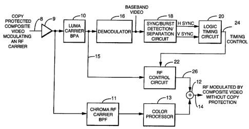
As depicted in the FIG. l, an RF carrier signal modulated by a composite
video signal and containing copy protection signals, is supplied on a lead 8
to a
luminance RF carrier bandpass filter (BPF) 10 and to a chrominance RF carrier
BPF 11
via a suitable amplifier 9. The latter BPF 11 supplies a chrominance signal to
a
summing circuit 12 via a conventional color processor circuit 13. The
chrominance
signal path is illustrated herein to show the manner in which the color signal
is
reassembled with the RF carrier signal in
8
CA 02278777 1999-07-26
WO 98/34401 PCT/US98I02474
which the copy protection :>ignals have been removed or otherwise defeated in
accordance
with the invention, to provide a RF carrier with modulating composite video
signal or an
output lead 14.
The RF carrier signal containing some form of modulating copy protection
signals
such as discussed above, is supplied via the luminance BPF 10 and a lead 15 to
a
demodulator circuit 16 which may be an FM, AM or other type of demodulator
commensurate with the modulated RF carrier signal. Thus, an RF carrier signal
supplied by
a playback VCR or satellite transmission is a frequency modulated signal,
while a RF
carrier signal from a television channel or cable, that is, off air, is an
amplitude modulated
to signal. Circuits 11 and 1:3 are generally used for VCR RF to RF dubbing
process of
previously mentioned.
To illustrate, FIG. lA exemplifies a waveform of a television line including a
vertical blanking interval (VBI) and depicting an RF carrier signal of, for
example, 61.25
megahertz (MHz), which is the broadcast frequency for channel 3 used
hereinafter in the
description of some of tree invention embodiments, wherein the RF carrier
signal is
amplitude modulated by a. video signal using, in this instance, a negative
modulation
process. It follows that the; peak white value of the video signal minimizes
the RF earner
signal while the sync tip value maximizes the RF carrier signal, as depicted
in the FIG. lA.
It is this RF carrier signal, modulated by given copy protection signals such
as, for example,
2o those disclosed in the patents referenced above, that is utilized in
accordance with the
invention in the RF domain to defeat the effect of the copy protection
signals.
Similarly, FIG. 1B c;xemplifies a television line waveform with a VBI,
depicting an
RF carrier signal which is frequency modulated by a video signal, such as
supplied by a
playback VCR, satellite transmission, etc. As depicted, the sync period is
represented by a
3.4 MHz frequency, the blanking level by 3.7 MHz frequency and peak white
level by 4.4
MHz frequency. As mentioned above, the RF carrier signal is utilized in the
invention
combination to detect and defeat the modulating copy protection signal in the
RF domain.
FIG. 1 C illustrates a typical RF frequency spectrum of an amplitude modulated
video signal on the picture or visual RF carrier frequency of 61.25 MHz, in
this example as
3o shown in Fig. lA. The modulating chroma signal is 3.58 MHz above the
picture RF carrier
frequency and thus is 64.8:5 MHz. The modulated aural RF carrier is 4.5 MHz
above the
picture RF carrier and thus is 65.75 MHz.
CA 02278777 1999-07-26
WO 98/34401 PG"T/US98/OZ474
FIG. 1D illustrates a RF frequency spectrum of a typical frequency modulated
recording system (FIG. 1B) such as supplied, for example, for a VHS or Beta
video
recorder. The luminance signal is depicted and the sync tip of the baseband
video signal is
modulated to 3.4 MHz (VHS). The peak white of the baseband video signal is
modulated
to 4.4 MHz (VHS). In essence, the recorder system is a voltage-to-frequency
converter
while the playback system is a frequency-to-voltage converter. It is noted
that the chroma
signal of the baseband video signal centered around 3.58 MHz is frequency
converted to a
lower frequency of, for example, 629 kilohertz (KHz) and is recorded onto the
medium.
Continuing now with FIG. 1, the demodulated baseband video signal from the
1o demodulator circuit 16 is supplied to a sync/burst detection/separation
circuit 18 which
generates vertical sync (V sync) signals at vertical or field rate, horizontal
sync (H sync)
signals at horizontal line rate, or color burst signals. The signal is
supplied to a logic timing
circuit 20 which supplies a timing control signal to a RF control circuit 22
on a lead 24.
The original RF carrier signal with modulating copy protection signals, that
is, anti-copy
pulses or color stripe signals, also is supplied to the RF control circuit 22
via the lead 15.
The RF control circuit 22 is steered by the timing control signal on the lead
24 to
selectively modify the incoming RF carrier signal in one of various techniques
in
accordance with the invention, such that the output RF carrier signal supplied
to the
summing circuit 12 via an output lead 26 no longer contains effective copy
protection
2o signals. That is, the anti-copy pulses or color stripe signals have been
removed and/or
disabled to enable a subsequent acceptable recording of the respective video
signal. As
previously mentioned, the copiable luminance signal on lead 26 is combined
with the
chroma signal by the summing circuit 12 to provide the composite video signal
without
copy protection on the output lead 14. Various methods and circuits for
performing the
modification to the RF carrier in accordance with the invention are
illustrated and disclosed
with reference to the following FIGS. 1 E, 2-5.
FIG. lE illustrates a system for defeating copy protection signals in the AM
RF
domain while further preserving the aural RF Garner portion of a modulated RF
carrier
signal if, as may happen, the aural RF carrier is degraded by the copy
protection defeating
3o process. To this end, copy protected video that has AGC and pseudo sync/and
or color
stripe burst protection signals is amplitude modulated on an RF carrier to
provide, for
example, the modulated RF carrier signal on lead 15 of FIG. 1. The signal is
supplied to a
line location/timing circuit 28, to a RF carrier processing circuit 29 and to
an aural RF
/V
CA 02278777 1999-07-26
WO 98134401 PCT/US98/02474
carrier BPF 30. The line loc;ation/timing circuit 28 corresponds to the
circuits 16, 18, 20 of
FIG. 1 and provides a timing control signal similar to that on the lead 24.
The RF carrier
processing circuit 29 is the equivalent of the RF control circuit 22 of FIG.
l, and combines
with the circuit 28 of FIG. lE to sufficiently defeat the AGC and/or pseudo
sync and/or
color stripe burst that has. been modulated onto the RF carrier, as is fully
described
hereinbelow in FIGs. 2, 4, .'i. Defeating the modulated copy protection
signals may cause
some degradation in the aural RF carrier portion of the RF carrier signal. To
preserve the
aural RF carrier, the band pass filter 30 is used to supply via a lead 31 just
the aural RF
carrier signal (FM audio 4..5 MHz above the visual carrier, for example) to a
summing
to circuit 32. The output of the processing circuit 29 on a lead 34 is a
modulated video with
defeated modulated copy protection signals but with a possibly degraded aural
RF carrier.
The output on lead 34 is supplied to an aural carrier notch filter 36. The
output of filter 36
is RF modulated video on a lead 37 with the modulated copy protection signals
defeated
suffciently, and with no, or little, aural RF carrier. The summing circuit 32
combines the
RF carrier signals on leads 31, 37, to yield an output RF carrier signal on a
lead 38 with
program video and audio RF carriers intact but with modulated copy protection
signals
defeated.
It may be seen that circuits 30, 32 and 36 are optional if audio quality in
the RF
carrier signal supplied by the processing circuit 29 is adequate. Thus, the RF
earner signal
on the lead 34 is an alternative output for the RF carrier signal on the lead
38.
The circuit of FIG. 1 further illustrates the means by which a video signal
modulated RF carrier signal can be modified in the RF domain to add copy
protection
signals onto the RF carrier signal. To this end, the RF control circuit 22 of
FIG. 1 may be
used to insert as, for exarnple, by modulating, RF carrier signals to replace
or modify
2s portions of the RF carrier envelope such that when the RF carrier signal on
the lead 26 is
demodulated, copy protectiion signals will appear to prevent copying.
Basically, the RF
carrier signal on the lead 15 in, for example an AM system, is modulated with
a video
signal not containing copy protection pulses, and is supplied to the
corresponding (AM)
demodulator circuit 16 andi the RF control circuit 22. The circuits 18 and 20
generate
so baseband copy protection signals on the lead 24 to modify the RF carrier
envelope in the
circuit 22. For instance, portions of the RF carrier signal are enhanced in
amplitude to
generate pseudo-sync signals modulating the coincident RF carrier, while
portions of the
RF carrier signal following l:his enhanced carrier amplitude are diminished to
generate AGC
CA 02278777 1999-07-26
WO 98/34401 PCT/US98I02474
pulses modulating the coincident RF carrier. The RF carrier signal on the lead
26 then
contains copy protection signals modulating an RF carrier. Other copy
protection signals
such as, for example, the color stripe burst signals of previous discussion
above, and
disclosed in the U.S. Patent No. 4,577,216 of previous mention, may be applied
in a similar
manner in the RF domain.
If FIG. 1 is an FM system, then the RF control circuit 22 will be used to
modify the
carrier frequency of the RF carrier signal on the lead 15, whereby portions of
the RF carrier
will be decreased in fr~uency to represent pseudo-sync signals frequency
modulating the
coincident RF carrier, followed by portions of the RF carrier that are
increased in frequency
1o to represent AGC pulses frequency modulating the coincident RF carrier.
FIG. 2 illustrates in further detail alternative embodiments of the invention
of FIG.
l, which embodiments receive an RF Garner signal via a television transmission
channel,
that is oil air, or via a cable system, etc., which RF carrier signal has
been, by way of
example only, AM modulated to include copy protection signals which inhibit
the copying
of the respective video signal. In this example, the RF modulated carrier
signal includes a
carrier of 61.25 megahertz (MHz) and an aural FM carrier signal of 65.75 MHz
as depicted
in FIG. 1C, as well as the copy protection signals. The modulated RF carrier
signal with
copy protection signals is supplied via a lead 40 to an amplifier 42, whose
output is
supplied via a lead 43 to an amplifier/AM detector/low pass filter circuit 44.
The AM
2o detector portion of the circuit 44 provides recovery of the baseband video
signal, while the
low pass filter at the output of circuit 44 removes the residual visual
carrier frequency from
the baseband video signal. The resulting baseband video signal is supplied to
a sync
separator circuit 46 which provides at its outputs a horizontal sync (H sync)
signal or pulse
and a vertical sync (V sync) signal or pulse on respective leads 48, 50. The H
sync signal
on lead 48 thus includes pseudo-sync anti-copy signals or pulses as well.
Leads 48, 50 are
coupled to a logic timing circuit 52 which generates a signal indicative of
the presence of
the television lines which contain the copy protection signals. Thus, circuit
52 effectively
comprises a line locator circuit which generates, for example, a low logic
level on a lead 54
during an active video line in which anti-copy signals are present which, in
the example
3o herein, are lines 10 through 20 in the vertical blanking interval. A high
logic level is
provided on the lead 54 during the presence of the normal sync and color burst
signals in
the vertical blanking interval as well as during the active television field.
Lead 54 is
coupled to a control input of a RF switch 56.
CA 02278777 1999-07-26
WO 98/34401 PCT/US98I02474
By way of background, certain portions of a normal viewing field defined by a
video
signal typically are not used for defining the actual picture. More
specifically, the
horizontal scan lines immediately adjacent to those portions of a video signal
defining
' vertical blanking intervals axe not used in typical television monitors or
sets to define the
picture. Therefore those sil;nal portions immediately adjacent to vertical
blanking intervals
are also available in their entirety for the addition of copy protection
signals. Thus, insofar
as this invention is concerned, such signal portions are also considered part
of the vertical
blanking intervals, and the term "vertical blanking interval" as used herein
encompasses the
same.
The modulated RF carrier signal supplied by the amplifier 42 also is supplied
via the lead
43 to an aural RF carrier notch filter circuit S7. To this end, lead 43 is
coupled to a
positive input of a RF differential amplifier S8 and to a filter network,
formed of resistors
60, 62 inductor 64 and capacitor 66, which network thence is coupled to an
inverting input
of the RF differential a.mpLifier 58. The notch filter circuit S7 herein is
used to prevent
degrading the aural RF carriier while providing for the defeat of the copy
protection signals
used to modulate the RF carrier signal. The junction of the resistors 60, 62
is coupled to
one terminal of the RF switc;h S6. A second terminal of the switch S6 is
coupled to ground.
The output of the RF differential amplifier S8 provides an output signal from
the circuit of
FIG. 2 on a lead 68, which output signal comprises a RF carrier signal in
which the copy
2o protection signals have been attenuated and which thus can be supplied to a
recording VCR
to provide an acceptable copy of the video signal.
To this end, the RF' switch S6 is maintained in an off condition by the low
logic
level on the lead S4 during the active video tines 10 through 20 when the copy
protection
signals axe present. During this portion of the vertical blanking interval,
the notch filter
2s circuit S7 is active to thereby prevent degrading the aural RF carrier,
while the video RF
carrier signal envelope is severely attenuated in the line intervals when the
RF Garner
modulating anti-copy signals are present. The attenuated RF carrier is
supplied as the
_ output signal on the lead 68. During the video lines and the active
television field when the
copy protection signals are absent, the RF switch S6 is coupled to ground via
a high logic
30 level on lead S4 to disable the notch filter circuit S7. During this
interval, the original RF
Garner signal on lead 43 is supplied as the output of the RF differential
amplifier S8 on the
lead 68. Thus, combining the two signals provides a modified or re-assembled
video
modulated RF carrier signal without the anti-copy signals, when demodulated
subsequently
~3
CA 02278777 1999-07-26
WO 98134401 PCT/US98J02474
as, for example, by a record VCR. It may be seen that, in this embodiment of
the invention,
the RF envelope is attenuated when the copy protection signals are present
without
affecting the aural RF carrier signal that is at a frequency of about 4.5 MHz
above the
visual RF carrier frequency, which is an additional advantage of the above
embodiment of
FIG. 2.
In an alternative technique employing in part the circuitry in FIG. 2, the
notch filter
circuit 57 and RF switch 56 are dispensed with and the modulated RF carrier
signal on the
lead 43 is supplied (via a dashed line portion) to an input of a RF voltage
control amplifier
or modulator 70. The line location, i.e., timing control, signal from the
logic timing circuit
52 is supplied via the lead 54 (and a dashed line portion) to a control input
of the RF
modulator 70. Thus, during the active video lines, for example, lines 10-20,
in the vertical
blanking interval, the peak envelope of the anti-copy signals modulating the
RF carrier may
be suppressed via the RF modulator 70 in response to the signal on the lead
54. It follows
that a re-assembled RF carrier signal is provided on an output lead 72 via an
amplifier 74 in
which the copy protection signals are disabled. In this embodiment, the aural
RF carrier
signal may be somewhat attenuated during suppression or attenuation of the RF
envelope
of the anti-copy signals. However, the aural RF carrier signal should still be
sufficient in
amplitude to not cause momentary losses of the audio signal, i.e., audio "drop
outs".
In a fi~rther alternative technique employing in part the circuitry of FIG. 2,
the notch
2o filter circuit 57, the RF switch 56 and/or the RF modulator 70 are
dispensed with and the
modulated RF carrier signal on lead 43 is supplied (via a dashed line portion)
to an input
terminal of a RF switch 76. A second RF source such as a RF carrier modulated
by a noisy
color signal, a RF carrier modulated by a color bar signal, an unmodulated RF
carrier or a
modulated RF carrier or other signal without sufficient anti-copy signals, is
supplied via a
lead 78 to a second terminal of the RF switch 76. The second replacement
signal may in
fact be no signal at all, including an RF signal of sufficiently low value
which likewise
induces a dropout during the period of the copy protection signals, which
effectively blanks
them out. In this alternative, the line location signal on the lead 54 is
supplied to the RF
switch 76 as a switch timing control signal, whereby the modulated RF carrier
signal on
lead 43 is replaced during the period of the copy protection signals with one
of the selected
RF signals on lead 78 which lacks any copy protection signals. The resulting
re-assembled
output signal on an output lead 80 of the RF switch 76 thus does not contain
anti-copy
signals whereby acceptable recordings can ~ made of the video signal.
Alternatively, an
CA 02278777 1999-07-26
WO 98134401 PCT/US98/02474
aural band pass filter 79 andl summing junction 81 may be employed to provide
the aural RF
carrier on the lead 78 from the lead 40 (as shown in a dashed line portion) so
that there is
no disruption in the aural RF carrier on output lead 80 when the RF switch 76
switches
from the RF carrier signal on lead 43 to the replacement carrier signal on
lead 78.
As previously discussed, the techniques and circuitry of FIG. 2 provide timing
and
modifying means operating in the RF domain for disabling copy protection
signals
previously embedded in a video signal using, in this instance, an AM recording
process
such as commonly done, for example, in an off air video transmission or cable
transmission
system.
1o Referring to FIGs. 3~A, 3B, the techniques and circuitry provide means
operating in
the RF domain for similarly disabling copy protection signals, but in a video
signal derived
via a FM recording system such as, for example, a dual deck videotape recorder
system
(i.e., VCR) employing RF to RF dubbing, or via a satellite system, etc. To
this end, in FIG.
3A a luminance RF Garner signal which is frequency modulated (FM) is supplied
to a
preamplifier/equalizing amldifier circuit 90 via an input lead 92 and thence
to a limiter
amplifier/FM detector circuit 94. The resulting baseband video signal is
supplied to a
lowpass filter/de-emphasis circuit 96 wherein the signal is filtered and de-
emphasized to
provide a baseband video luminance demodulated signal for input to a sync
separator
circuit 98 and to provide the luminance demodulated signal on a lead 100. The
sync
2o separator circuit supplies a composite H sync with anti-copy pseudo-sync
signals via a lead
102, and a V sync signal via a lead 104.
The composite H and pseudo-sync signal is supplied to a non-retriggerable one-
shot
multivibrator 106 of about 50 microseconds, which supplies a pulse to an AND
gate 108
which begins at the trailing edge of H sync and extends to the end of an
active horizontal
2s television line. Thus, the. non-retriggerable one-shot 106 provides a
signal which is
indicative of the presence of active television line pixels. The one-shot 106
also ignores
triggering on the anti-copy ;pseudo-sync pulses. The V sync signal is supplied
to a one-shot
110 of about 6 television limes duration, and thence to another one-shot 112
of about 10
television lines duration whiich generates a vertical rate pulse that is, for
example, logic high
from television lines 10 through 20 and thus is a logic high during the
presence of RF
Garner modulated by the anti-copy pulses in the lines. The output of one-shot
112 is
supplied to the AND gate l; 08 which provides a line locator signal, via a
lead 114 that is a
9~
CA 02278777 1999-07-26
WO 98/34401 PCT/US98/02474
logic high during the presence of pseudo-sync and AGC pulses, excluding
however, normal
H sync pulses.
Referring to FIG. 3B, the luminance demodulated signal on lead 100 (FIG. 3A),
is
supplied to a video clamping circuit 116, which clamps the luminance signal to
sync tip
s voltage and supplies the signal to one terminal of a switch 118. The other
terminal of the
switch 118 is grounded. The line locator signal on the lead 114 from FIG. 3A
is used to
control the switching of the switch 118. The output of switch 118 is coupled
to an
inverting input of a comparator amplifier 120 and a non-inverting input of a
comparator
amplifier 122. The non-inverting and inverting inputs of comparator amplifiers
120, 122,
to respectively, are coupled to threshold voltages Vbl and Vb2. In response to
the line
locator signal on lead 114, a clamped luminance signal is supplied to the
comparator
amplifiers 120, 122 during the presence of pseudo-sync and AGC pulses.
Amplifiers 120,
122 in turn, generate logic high levels PS and AGC coincident with the RF
carrier
modulating pseudo-sync (PS) and AGC pulses, respectively, and output the
corresponding
15 logic signals on respective leads 124, 126, as well as to one input of
respective AND gates
128, 130. The voltages Vbl and Vb2 are selected commensurate with the sync tip
voltage
level and the AGC pulse voltage level, respectively. The PS and AGC logic
signals also are
supplied to pulse narrowing circuits 132, 134 respectively, each formed of
resistors coupled
to second inputs of respective AND gates 128, 130 and capacitors coupled from
respective
2o second inputs to ground. The AND gates 128, 130 supply narrowed pulse width
logic
signals NPS and NAGC from the respective PS and AGC signals, on leads 136,
138.
It is to be understood that the AGC anti-copy pulses alternatively may be
clustered
at selected timing positions along the "back porch" of the vertical blanking
interval such as
described in the U.S. Patent No. 4,819,098 of previous mention, and that the
present
25 invention further contemplates the defeat of such clustered copy protection
modifications
to the video signal.
The line locator signal on lead I 14 and signals PS, AGC, NPS and NAGC on
leads
124, I26, 136, 138 respectively, are coupled as inputs to a logic combining
circuit 140
which, in turn, supplies a timing control signal to a RF switch 142 via a lead
143. The
30 luminance RF carrier signal of FIG. 3A is coupled via the lead 92 and a
lead 144 to a
terminal of the switch 142. A signal source generator 146, including an
oscillator or an RF
frequency source, is coupled via a jumper circuit 148 to a second terminal of
the RF switch
CA 02278777 1999-07-26
WO 98134401 PCTIUS98/OZ474
142. The output terminal of RF switch 142 is coupled to a low pass filter 150
of about 7
MHz, which provides the output from FIGs. 3A, 3B on a lead 152.
During the period of RF carrier modulating anti-copy signals, e.g., pseudo-
sync
and/or AGC pulses, the luminance RF carrier signal on lead 144 to the RF
switch 142 is
replaced in response to the timing control signal from the logic combining
circuit 140 by a
signal supplied by the signal source generator 146 comprising a frequency that
represents
blanking level, an attenuated pseudo-sync amplitude or a narrowed pulse width
pseudo-
sync signal (when demodulated in a record VCR or satellite tuner). The
replacement signal
also may be no signal, or an RF signal of low value, whereby essentially a
dropout is
to induced by the resulting reduced carrier level at the time of occurrence of
the copy
protection signals used to n-~odulate the RF carrier signal, thereby
effectively blanking them
out. The timing control signal, in turn, is a reflection of the line locator
signal on lead 114,
and the PS signal on lead 124 or the NPS signal on the lead 136, respectively.
The PS
signal causes a pulse level shifting or attenuation affect while the NPS
signals causes a
pulse narrowing effect. Likewise, if the control signal AGC on lead 126 or
NAGC on lead
138 are used along with the line locator signal on lead 114 to control the RF
switch 142 via
the logic combining circuit 140, the luminance RF carrier signal on lead 144
is replaced by
a frequency which produces AGC pulses of attenuated amplitude or AGC pulses of
narrowed pulse width, respectively, when demodulated in a record VCR or
satellite tuner.
2o Thus, the line locator signal on lead 114 is used to switch a RF signal
into the luminance
RF carrier signal to thus replace the portions of the television lines
containing RF carrier
modulating anti-copy signals with any active television line signal which
would render
recordable copies of the video signal when FM detected subsequently in a
dubbing process.
The re-assembled signal from the RF switch 142 is supplied to the low pass
filter 150 which
removes any discontinuities in the RF carrier waveform. The resulting re-
assembled
luminance RF carrier signal with copy protection signals disabled is supplied
via the lead
152 to, for example, the RF' luminance FM input of a record VCR, whereby an
acceptable
recording may be made.
An alternative technique employing the circuitry of FIGS. 3A, 3B, provides a
shift
or alteration in the frequency of the signal on lead 144 to cause a
corresponding level shift
in the copy protection signals when subsequently demodulated. To this end, the
luminance
RF carrier signal on lead 144 is supplied to a single sideband (SSB) modulator
154 and
thence to a second input ~of the jumper circuit 148. An oscillator 156 of
about 100
CA 02278777 1999-07-26
WO 98/34401 PCT/US98/02474
kilohertz (KHz) or more frequency is coupled to the SSB modulator 154. The
modulator
154 is a single sideband AM modulator with an upper sideband output.
Accordingly, when
the output of the modulator 154 is switched into the luminance RF carrier
signal in
response to the line locator signal on the lead 114 and timing control signal
on the lead 143,
the positive frequency of the oscillator 156 effectively is added to the
luminance RF Garner
signal. As a result, the level of pseudo-sync pulses in the modified luminance
RF carrier
signal supplied to a record VCR via the output lead 152, will be level shifted
when
demodulated, thus allowing acceptable recordings to be made.
FIG. 4 depicts an alternative embodiment of the invention for removing copy
1o protection signals from a copy protected modulated RF carrier signal using
techniques in
the RF domain. To this end, a modulated RF carrier signal such as derived from
off air via
a television channel, cable system, etc., wherein the RF carrier has been AM
modulated to
include copy protection signals, is supplied to a DC restoration circuit 170
via a lead 172.
The circuit 170 includes a capacitor 174, a resistor 176 and a diode 178
coupled at a
common junction and thence to a non-inverting input of a comparator amplifier
180. The
free ends of the resistor 176 and diode 178 are coupled to a supply voltage
and to ground,
respectively. The DC restoration circuit 170 thus DC restores the RF envelope
to its peak
value, i.e., the sync tip RF envelope value. The restored RF carrier signal is
supplied to the
comparator amplifier 180 which slices the peak RF just below its maximum as
established
2o by a threshold voltage Vth applied via a lead 182 to an inverting input of
comparator
amplifier 180. The comparator amplifier 180 supplies a burst of RF, coincident
with the H
sync and V sync which modulate the RF carrier signal, to a low pass filter
184. The filter
184 filters out the RF components to supply a baseband composite sync signal
including H
sync, V sync and pseudo-sync signals to a logic timing circuit 186 and to a
second low pass
filter 188, via a lead 187. The filter 188 retrieves the V sync signal and
supplies it to the
logic timing circuit 186 via a lead 189. The latter circuit 186 generates on a
lead 190 a
timing location or timing control signal which identifies the location of the
video lines and
associated RF carrier modulating anti-copy signals, i.e., the pseudo-sync and
AGC pulses.
The modulated RF carrier signal on the lead 172 also is supplied to a depth of
3o modulation circuit 192, and to a RF carrier regeneration circuit 194 which
thence also is
coupled to the circuit 192. The RF Garner regeneration circuit 194 includes a
phase lock
loop (PLL) and generates on a lead 198 a continuous wave RF carrier of
constant value
and of a frequency similar to the frequency of the modulated RF carrier signal
on lead 172.
CA 02278777 1999-07-26
WO 98/34401 PCT/L1S98/02474
The depth of modulation circuit 192 provides means for changing the depth of
modulation
of the RF carrier envelope in response to the timing location signal on lead
190, and for
then supplying the modified RF carrier signal via an output lead 196. Thus, in
response to
the timing location of the RF carrier modulating pseudo-sync pulses, and/or
the AGC
pulses, the depth of RF carrier modulation can be changed by the circuit 192
to add or
subtract the continuous wave Garner of the regeneration circuit 194 to or from
the
modulated RF carrier signal on lead 172 during the timing intervals of the
pseudo-sync or
AGC pulses. The alteraticms in the depth of RF carrier modulation can be
achieved by
making changes in the gain, or by level shifting, blanking, narrowing, and/or
adding or
lU subtracting RF carrier to the embedded anti-copy signals. In this manner,
the pulses which
prevent copying are modified to make them subsequently transparent to the
various circuits
of, for example, a record VCR coupled to the output lead 196, thereby allowing
acceptable
recordings of the video signal in accordance with the invention.
In an alternative modification to FIG. 4, the low pass filter to retrieve the
composite
H and pseudo-sync pulses can be replaced by using instead a one-shot
multivibrator timing
circuit to trigger a pulse at l:he output of the comparator amplifier 180.
Furthermore, if the
copy protected modulated IRF carrier is large in signal level, the comparator
amplifier 180
can be replaced by a diode or transistor to perform partial RF envelope or
power detection
to effectively achieve the results of the amplifier 180.
2o FIG. 4A illustrates further details of the logic/timing circuit 186 of FIG.
4, wherein
similar components are similarly numbered and labeled. Thus, the V sync signal
from the
low pass filter 188 (FIG. 4) is supplied via the lead 189 to a one-shot
multivibrator 200 and
thence to an AND gate 2.02 via a second one-shot multivibrator 204. Likewise,
the
composite sync signal from the low pass filter 184 (FIG. 4) is supplied via
the lead 187 to a
one-shot multivibrator 206 and thence to the AND gate 202. The one-shots 200,
204 and
206 have time durations of about 6 television lines, about 10 television lines
and 50
microseconds, respectively. The one-shot 206 is triggered by the trailing edge
of each H
sync pulse but is immune to the edge of pseudo-sync pulses. The signal from
the one-shot
204 comprises vertical rate pulses indicative of active television lines 10
through 20
modulating the RF carrier, while the signal from the one-shot 206 is
indicative of the active
television line pixels modulating the RF carrier. An output lead 208 from the
AND gate
202 provides a line locator signal formed of logic high pulses which are
coincident with the
AGC and PS pulses but not necessarily with normal H sync pulses modulating the
RF
?9
CA 02278777 1999-07-26
WO 98134401 PCTII1S98102474
carrier. The line locator signal on the lead 208 is indicative of active
television line pixels in
or adjacent to the vertical blanking interval for lines 10 through 20
containing the anti-copy
pulses. As may be seen, the components 200-206 are similar to the components
106-112
of FIG. 3A, and the line locator signal on lead 208 is similar to the line
locator signal on the
s lead 114 and is used for similar purposes.
The composite sync signal, with PS pulses, also is supplied to an AND gate
210,
and the line locator signal on the lead 208 is supplied to the AND gate 210 as
well as to a
logic combining circuit 2v 2. The AND gate 210 supplies logic high pulses
coincident with
PS pulses on a lead 214, and also provides an input to a one-shot
multivibrator 216 of 3
1o microseconds duration, which then supplies pulses coincident with AGC
pulses on a lead
218. The PS and AGC. logic level pulses on leads 214, 218 are supplied as
timing signals to
the logic combining circuit 212 along with the line locator signal on lead
208. The logic
combining circuit 212 supplies the timing control signal of previous
description in FIG. 4
on the lead 190, which signal is coincident with the RF carrier modulated by
AGC and PS
1s pulses in the associated television lines.
FIG. 4B depicts an example of the depth of modulation circuit 192 of FIG. 4,
which
example depicts a switching circuit 230 that enables changing the depth of RF
carrier
modulation of the incoming modulated RF Garner signal containing copy
protection, which
is supplied via the lead 172 of the FIG. 4. To this end, the AGCP signal on
lead 218 of
2o FIG. 4A is supplied to control the switching circuit 230 such that the
regenerated
continuous wave RF (visual) Garner signal on lead 198 of FIG. 4, preferably
including the
aural RF carrier from the signal on the lead 172, is gated into the modulated
RF carrier
signal during the time that modulated AGC pulses are present in the former
signal. Thus,
the switching circuit 230 "fills in" the RF carrier which is pinched off by
the modulating
2s anti-copy AGC pulses. The resulting RF carrier signal on the output lead
196 of previous
mention in FIG. 4, has a reduction in the depth of modulation during the
period of the RF
carrier modulated by AGC pulses. It follows that in a subsequent recording
process of the
respective video signal, the altered or suppressed AGC pulses allow the
recording of an
acceptable copy. Alternatively, the signal on lead 198 can be the aural RF
carrier only,
3o whereupon the output signal on the lead 196 contains blanked or attenuated
visual RF
carrier during the period that the RF carrier modulating copy protection
signals are present
in the RF Garner signal on the lead 172.
g-o
CA 02278777 1999-07-26
WO 98/34401 PCT/US98/OZ474
FIG. 4C depicts an alternative example of the depth of modulation circuit 192
of
FIG. 4, which is similar to t:he example of FIG. 4B but which utilizes the PS
signals instead -
of the AGC signals to disable the RF carrier modulating anti-copy pseudo-sync
signals
providing the copy protection. To this end, the modulated RF carrier signal on
the lead
172, FIG. 4, is supplied to a~ summing circuit 234 of FIG. 4C. The regenerated
continuous
wave RF carrier signal on the lead 198, FIG. 4, is supplied to an inverter 236
and thence to
one 'input terminal of a switching circuit 238. The other input terminal of
switching circuit
238 is coupled to ground, a.nd switching control is provided by the PSP signal
on the lead
2 i 4 of FIG. 4A. The output of the switching circuit 23 8 is coupled to a
second input of the
1o summing circuit 234, and supplies thereto an inverse phase visual RF
carrier signal which is
regenerated or derived during the time interval of the RF carrier is modulated
by pseudo-
sync signals. This inverse carrier signal is combined with the modulated RF
carrier signal
on lead 172 by the summing circuit 234. The resulting re-assembled RF carrier
signal on
the output lead 196 (also F'IG. 4) has reduced peak carrier levels for pseudo-
sync pulses
such that, when subsequently detected by the associated circuitry in, for
example, a VCR,
the reduced pseudo-sync pulse amplitudes allow the making of an acceptable
recording.
The circuit of FIG. 4C also preserves the aural RF carrier signal during the
switching
process of the switching cir<;uit 238 in response to the PSP on lead 214.
In an alternative to the PS pulse suppression technique of previous
description in
2o FIG. 4C, if the pulse widths. of the pseudo-sync pulses of the output of
the AND gate 210
on the lead 214 are narrowed instead, then when the PSP signal is applied to
control the
switching circuit 238, FIG. 4C, the anti-copy pseudo-sync pulses of the
modulated RF
carrier output on lead 196 likewise are narrowed. The result is that the
narrowed pseudo-
sync pulses are not detectable by a subsequent VCR whereby an acceptable
recording is
2s permitted.
FIG. 4D depicts another alternative example of the depth of modulation circuit
192
of FIG. 4. This circuit reduces the peak modulation(even to about zero carrier
amplitude)
of the PS pulses and/or reduces the depth of modulation of the RF carrier
envelope
coincident with the AGC pulses by way of an RF modulating, that is, a gain
control,
3o technique. In addition, the circuit of FIG. 4D also may be used to reduce
the overall RF
carrier modulation of either or both the AGC and pseudo-sync modulated RF
envelope
such that when demodulated or detected by, for example, a record VCR, results
in a video
signal with a combination of attenuated and level shifted pseudo-sync pulses
with
a~
CA 02278777 1999-07-26
WO 98/34401 PCT/US98/02474
attenuated AGC pulses relative to the program video during the active
television field
signal, which permits an acceptable recording. Alternatively,the depth of
modulation circuit
192 may be used to remove the RF carrier signal during copy protection signal
modulation
as to allow a recordable copy.
s To this end, referring first to FIG. 4A, the inverted versions of the timing
signals
labeled line locator on lead 208 and PSP on lead 214, and the timing signal
AGCP on lead
218, are supplied to the inputs of a summing amplifier 240 in FIG. 4D. The
output of the
summing amplifier 240 is supplied to an AM RF modulator circuit 242 along with
the
modulated RF carrier signal on the lead 172 (FIG. 4) which contains the RF
carrier
modulating anti-copy pulses. The summing amplifier 240 thus controls the gain
of the RF
modulator 242 in response to one of the signals input thereto on the leads
208, 214 and
218. More particularly, the line locator signal causes the attenuation and/or
level shifting of
pseudo-sync pulses when subsequently demodulated by, for example, a record
VCR. The
PSP signal causes reduced peak RF carrier in the output on lead 196 which
permits copying
I5 during the subsequent pseudo-sync modulation by record VCR circuitry.
Alternatively,
application of the AGC pulses cause the RF Garner level to be at an increased
Garner level
during the AGC pulse modulation which, when detected by a tuner circuit of the
record
VCR, results in reduced AGC pulse amplitudes. Thus, use of the circuit of FIG.
4D results
in the record VCR making an acceptable recording in which the copy protection
signals
2o have been disabled in accordance with the RF domain techniques of the
invention.
In an alternative RF domain technique, narrowing of the PSP and/or AGCP pulses
supplied on leads 214,218 provides correspondingly narrowed RF carrier
modulated by
pseudo-sync and/or AGC pulses which, when demodulated by the record VCR,
provide
similarly acceptable recordings of the video signal. ~ The narrowing of the
PSP and/or
25 AGCP pulses may be accomplished as depicted, for example, in FIG. 3B.
FIG. 5 illustrates a further embodiment of the invention, which embodiment
provides means operating in the RF domain for disabling copy protection
provided by the
color stripe effect of previous discussion, wherein the color burst integral
with a video
signal is phase modulated in some manner to prevent acceptable copying.
Referring to the
3o block diagram, a modulated RF carrier signal, containing color stripe copy
protection
signals, is supplied via an input lead 250 to a detector circuit 252 for
detecting an RF
carrier modulated by color burst, to a RF carrier regeneration circuit 254, to
a phase lock
loop (PLL) 256 for providing a RF carrier with modulating color burst, and to
one input
a-a
CA 02278777 1999-07-26
WO 98134401 PCT/US98/02474
terminal of a RF switching circuit 258. The modulated RF carrier signal is
supplied from
off air via a television charnel, a cable system, etc., and in this example is
derived from
channel 3. The RF burst detector (i.e. at 64.83 Mhz) is coupled via a lead 260
to a logic
timing circuit 262 which thence provides a control signal to the RF switching
circuit 258
s via a lead 264. The lead 260 also is coupled as a control signal to the RF
modulated by
burst PLL 256. The output of the RF carrier regeneration PLL 254 is coupled to
one input
of a summing circuit 26b via a lead 268. The output of the RF modulated burst
PLL 256 is
coupled to a second input of the summing circuit 266 via a lead 270. The
output of the
summing circuit 266 is ~supp~lied via a lead 272 to a second input of the RF
switching circuit
258, whose output supplies a RF carrier signal on an output lead 274 wherein
the color
stripe copy protection .signal has been disabled thereby allowing the
subsequent making of
acceptable recordings. Accordingly, the circuit of FIG. 5 operates in the RF
domain to
provide a regenerated color burst modulated onto a RF carrier signal which,
when
demodulated, contains ineffective color stripe burst signals which have been
sufficiently
IS modified to permit the recording of an acceptable copy.
The burst detector .circuit 252 of FIG. 5 provides circuitry which derives a
color
burst (CB) control signal from the incoming RF modulated carrier on the lead
250
containing color stripe color protection modulated onto the RF earner. To this
end, FIG.
SA illustrates by way of example only, such a circuitry. The modulated RF
carrier signal
2o from, for example, the channel 3 broadcast station, is supplied on lead 250
to a bandpass
filter (BPF) 280. In this example, the RF carrier of channel 3 has a frequency
of 61.25
MHz modulated by the color burst frequency of 3.58 MHz (for the NTSC
standard),
whereby the modulated RF earner signal on lead 250 has a frequency of 64.83
MHz. Thus,
the BPF 280 filters out the RF carrier frequency of 61.25 MHz to extract via
the BPF 280
25 onto a lead 281, a signal coincident with the RF carrier modulated by color
burst but having
a frequency of 64.83 MHz. This signal is supplied to a one-shot multivibrator
282 of, for
example, 50 microseconds duration. The one-shot 282 triggers off the leading
edge of the
filtered 64.83 MHz signal and is immune to any color signal in the 64.83 MHz
signal since
the pulse duration of 50 microseconds extends the pulse the full time duration
of an active
3o television line. The signal output from the one-shot 282 thus contains only
a 50
microsecond pulse triggered from the RF modulated by color burst. This latter
signal is
supplied to a one-shot multivibrator 284 of 2 microseconds duration which is
triggered by
the leading edge of the 50 nucrosecond pulse to provide a signal coincident
with color burst
a3
CA 02278777 2001-07-11
but at 64.83 MHz, which thus represents the timing location of the RF carrier
modulated
by color burst. Thus, the output of the one-shot 284 is a modulating burst
location signal -
(BL) on the lead 260 (FIG. 5), which is unaffected by any other modulating
chroma signal,
is coincident with the RF carrier modulated by color burst occurrence, and
which is used
as a timing control signal to control the operation of the RF modulated by
burst PLL 256,
as described below. A similar BL, signal may be derived from the composite
sync signal
on the lead 187 of FIG. 4, or from the H sync signal derived from the circuit
16 of FIG. 1.
The burst location signal also is supplied via the lead 260 to the logic
timing circuit
262 which provides a BL related tuning control signal on the lead 264 for
switching the
switching means 258 in coincidence with the RF carrier modulating anti-copy
color stripe
signals contained in the modulated RF carrier signal. The circuit 262 may be
simply a
lead, or may be a logic circuit that derives a timing control signal which is
coincident with
the RF carrier modulated by color stripe bursts.
In FIG. 5, the RF carrier regeneration PLL 254 includes a phase lock loop
having a
61.25 MHz frequency matching the RF carrier frequency of the respective off
air
television channel, which in this example is channel 3. If other channels and
frequencies
are used, then the frequencies of the various PLL circuits are selected
accordingly. The
signal provided by the PLL 254 on the lead 268 is a continuous wave (CW) RF
carrier of
61.25 MHz which is supplied to the summing circuit 266 for combination with
the output
signal from the RF modulated by burst PLL 256.
The RF modulated burst PLL 256 is illustrated in FIG. SB in further detail,
and
includes in this example a gate circuit 286 which is coupled to the bandpass
filtered signal
on the lead 281, and is gated by the modulating burst location signal (BL) on
the lead 260,
FIGs. 5, SA. The gate circuit 286 supplies a resulting gated burst modulation
signal to a
PLL 288 of 64.83 MHz frequency, which PLL 288 corresponds to the phase lock
loop
portion of the RF modulated by burst PLL 256 of FIG. 5. The color burst
modulated
signal and its relationship to the visual RF carrier frequency is depicted in
the frequency
spectrum of FIG. SC. The PLL '?88 supplies a color burst modulated RF carrier
continuous wave signal on the lead 270. Due to the inertia of the PLL 288, any
color
stripe phase errors modulated onto the RF carrier are removed by the averaging
process of
the PLL.
As previously mentioned, the continuous wave RF carrier on the lead 268 is
combined with the continuous wave color burst modulated RF carrier on the lead
270 by
the summing circuit 266, to provide an RF modulated, color subcarrier
continuous wave
frequency on the lead 272, FIG. 5, which is supplied to the RF switching
circuit 258. In
24
CA 02278777 1999-07-26
WO 98/34401 PCT/U898I02474
response to the timing control signal on lead 264, the RF modulated, color
subcarrier signal
on lead 272 is inserted in t:he original modulated RF carrier signal which has
color stripe
copy protection, during the intervals that the color stripe modulation is
present. Thus, the
output lead 274 provides a RF carrier signal wherein the modulating color
stripe copy
protection signal is disabled, such that acceptable copies can be made
subsequently, for
example, by a record VCR.
It is to be understood that although the description herein of the various
embodiments of the FIGs. l -5 illustrates the invention techniques as
replacing or otherwise
modifying all the cycles of the copy protection waveforms modulated onto the
RF carrier
signal, the invention further intends that only portions of the RF carrier
modulating pseudo-
sync and/or AGC pulses, or of the color burst, or only a selected number of
the anti-copy
signals, need be replaced or modified to provide the intended disabling of the
copy
protection in the RF domain. Thus, for example, in the techniques wherein the
pseudo-sync
andlor AGC anti-copy pulses are being replaced or otherwise modified, only a
portion of
the pseudo-sync and/or A(iC pulses modulating the RF carrier signal need be
modified.
Alternatively, the modulating anti-copy pulses may be selectively narrowed
such that they
are not detectable subsequently by the VCR circuitry. Still fi~rther, only a
selected number
of the anti-copy signals rnay be replaced, altered, narrowed or otherwise
modified to
provide the same effect of disabling the anti-copy signals and thus the copy
protection.
2o Similarly, in the techniques wherein the RF carrier modulating color stripe
effect provides
copy protection, only a selected number of cycles of the subsequently
demodulated
waveform, or only a few lines containing color stripe copy protection, when
demodulated,
need be replaced or modified in the RF domain to cause similarly disabling the
process in
accordance with the inventiion. It should be known that varying the duty
cycle(narrowing)
and or frequency of the RF carrier during the copy protection signal
modulation can also
result in a recordable copy. This is analogous to the Quan et al United States
Patent
number 5,194,965. Also see pulse narrowing circuits such as FIG. 3B circuits
132 and
134. Also see frequency varying circuit such as in FIG 3B , circuit 154.
Likewise, the
amplitude level of the RF <;arrier during modulation from the copy protection
signals may
3o be varied (for example,eve:n to cause an RF drop out) as to allow a
recordable copy.
Accordingly, although the invention has been described herein relative to
specific
embodiments and alternatives thereto, various additional features and
advantages will be
~ ~i
CA 02278777 1999-07-26
WO 98/34401 PCT/US98/02474
apparent from the description and drawings, and thus the scope of the
invention is defined
by the following claims and their equivalents.
.26