Note: Descriptions are shown in the official language in which they were submitted.
CA 02278825 2006-09-05
Anti-reflective coating for a CRT having first and second optical thin films
in
combination with an adhesion layer
BACKGROUND OF THE INVENTION
Field of the Invention
This invention relates to an anti-reflection film and a cathode ray tube. More
particularly, it relates to an anti-reflection fihn that is able to improve
tightness of
adhesion of the thin optical film to a substrate, and to achieve anti-
reflection effects
over a wide wavelength range, and a cathode ray tube employing this anti-
reflection
,.. ,
filin.
Description of the Related Art
Up to now, an anti-reflection film has been used in the optical and in electro-
optical field where it is desirable or necessaxy to decrease the refractive
index on an
optical interface between air and glass. Specifically, the field of usage for
the anti-
reflection film covers a wide field encompassing a camera lens, a platen for a
copying
machine, cover glass for equipments, a panel for a cathode ray tube (CDT) and
other
display devices.
This anti-reflection film may be enurnerated by a fihn configured as shown for
exainple in Fig. 1. Tlus film is coinprised of a resin substrate 101, on a
major surface
1 a of which are sequentially formed a first layer 102 of SiOx, where x<2,
having a
thickness of 10 nm, a second layer 103 of ITO, having a thickness of 20 zun, a
third
layer of Si02, having a thickness of 25 nm, a fourth layer 105 of ITO, having
a
1
CA 02278825 1999-07-26
thickness of 60 run, and a fifth layer 106 of Si02, having a thickness of 100
nln.
This anti-reflection fihn has, however, an inconvenience that it has a multi-
layered structure with as many as five layers, and a thicker total fihn
thickness of 215
nm, so that it is difficult and pains-taking to manufacture, while being poor
in
productivity and high in production cost.
Thus, a demand is raised for an anti-reflection fihn having a smaller nuinber
of
layers. If the nuinber of layers is smaller, the number of layering steps is
decreased
to facilitate the production and improve the productivity as well as to lower
the
production cost.
In order to meet this demand, there has been proposed an anti-reflection film
of a dual structure having on a substrate a thin film mainly composed of TiN
and an
Si02 thin fihn of lower refractive index, as a second optical film, as
disclosed in
Japanese Laying-Open Patent H-9-156964, Japanese Laying-Open Patent H-9-165231
or in Japanese Laying-Open Patent H-9-73001.
However, this anti-reflection fihn, while having acceptable anti-reflection
characteristics, is not optimum in adhesion between the substrate and the thin
film,
irtainly composed of TiN, such that the film is susceptible to exfoliation and
difficult
to use practically.
SUMMARY OF THE INVENTION
It is therefore an object of the present invention to provide a practically
useful
anti-reflection fihn which has a slnall number of layers and high productivity
and
~
CA 02278825 1999-07-26
which is easy and siunple to manufacture while being low in production cost
and
superior in anti-reflection characteristics.
It is another object of the present invention to provide anti-reflection sheet
and
a cathode ray tube employing this anti-reflection fihn.
According to the present invention, there is provided an anti-reflection fihn
wherein an adhesive layer is formed on a major surface of a resin substrate, a
first
optical thin film containing one or more of titaniuln nitride, hafnium nitride
or
zirconium nitride is formed on the adhesive layer, and wherein a second
optical thin
film having a refractive index of 1.35 to 1.7 is fonned on the first optical
thin filln.
Preferably, the adhesive layer is represented by the chemical formula of SiOõ
where x < 2. The adhesive layer may be formed of a compound represented by the
chemical fonnula of SiN X, where x < 4/3, or by, the cheinical formula of
SiON},, where
x<2andy<4/3.
If, when the adhesive is formed of a compound having the chelnical formula
SiOX, where x < 2, sufficient bonding strength between the resin substrate and
the first
optical thin fihn cannot be developed. If the value of x is too small, silicon
is
metallized to increase undesirably the optical absorption characteristics to
ilnpair the
anti-reflection characteristics.
In the anti-reflection fihn of the present invention, the adhesive layer may
predolninantly be composed of Ti.
In the anti-reflection film of the present invention, the physical film
thickness
CA 02278825 1999-07-26
of the adhesive layer is preferably not larger than 10 run and more preferably
1 to 7
nm. If the physical fihn thickness of the adhesive layer is thicker than 10
nm, optical
absorption characteristics of the adhesive layer become excessive to impair
undesirably the anti-reflection characteristics. If the physical film
thickness is thinner
than 1 nm, sufficient bonding strength between the resin substrate and the
first optical
thin film undesirably cannot be developed.
In the anti-reflection fihn of the present invention, the physical film
thickness
of the first optical thin fihn is preferably 5 to 25 run. If the physical film
thickness is
. ..
outside this range, sufficient anti-reflection characteristics cannot be
achieved.
In the anti-reflection fihn of the present invention, it is desirable for the
first
optical thin film to contain mainly titanium nitride and for titanium nitride
to be doped
with metal. This metal may be exemplified by tungsten and gold.
If the first optical thin fihn mainly contains titaniuin nitride, the first
optical thin
film desirably is electrically conductive.
In the anti-reflection film of the present invention, the first optical thin
film
preferably is colnposed of Si02, while the physical film thickness of the
second optical
thin film preferably is 60 to 110 nln. If the second optical thin fihn
colnposed of SiOz
is outside the above range, sufficient anti-reflection characteristics cannot
be obtained.
In the anti-reflection film of the present invention, a hard coating layer
preferably is fonned on the surface of the resin substrate facing the adhesive
layer,
while an adhesive layer preferably is fonned on the hard coating layer.
4
CA 02278825 1999-07-26
The above-described anti-reflection fihn of the present invention may be
arranged on the face plate surface of a display portion to constitute the
cathode ray
tube.
In the cathode ray tube of the present invention, it is preferred that the
first
optical thin film ofthe anti-reflection fihn predolninantly contains titanium
nitride, this
first optical thin fihn being electrically conductive and grounded.
In the anti-reflection fihn of the present invention, since the adhesive layer
is
fonned on the major surface of the resin substrate, the first optical thin
film containing
one or more of titaniuin nitride, hafniuln and zirconium nitride is fonned on
the
adhesive layer, and the second optical thin fihn having the refractive index
of 1.35 to
1.7 is fonned on the first optical thin fihn, the nulnber of layers is small
to facilitate
and simplify the manufacturing process to reduce the cost.
In the anti-reflection fihn of the present invention, since the adhesive layer
is
interposed between the resin substrate and the first optical thin fihn
containing one or
more of titanium nitride, hafrnium and zirconium nitride, the first optical
thin fihn is
not liable to be detached from the resin substrate to assure good practically
suitable
anti-reflection characteristics.
Therefore, in the cathode ray tube of the present invention, in which the anti-
reflection film of the present invention is arranged on the surface of the
face plate of
the display portion thereof, the anti-reflection characteristics are
silnilarly good and
practically suitable.
CA 02278825 1999-07-26
Also, in the anti-reflection film of the present invention, if the adhesive
layer
is fonned of a compound represented by the chelnical fonnula of SiOx, where x
< 2,
the first optical thin fihn is less liable to be detached from the resin
substrate.
If, in the anti-reflection film of the present invention, the first optical
thin fihn
mainly is composed of titaniuln nitride, and the first optical thin fihn is
electrically
conductive, the first optical thin film may be used as an electrically
conductive fihn in
place of the ITO layer used as an electrically conductive fihn in the
conventional anti-
reflection fihn.
, ..
Also, if, in,the anti-reflection film of the present invention, the first
optical thin
fihn is formed of titanium nitride, having strong absorption characteristics,
and the
anti-reflection film is arranged on the face plate surface of the cathode ray
tube, the
image displayed on the cathode ray tube can be iunproved in contrast.
In the anti-reflection fihn of the present invention, in which an adhesive
layer
is fonned on a major surface of a resin substrate, a first optical thin fihn
containing
one or more of titanium nitride, hafniuln nitride or zirconium nitride is
fonned on the
adhesive layer and in which a second optical thin film having a refractive
index of 1.35
to 1.7 is fonned on the first optical thin fihn, the number of layers is
small, so that the
manufacture may be facilitated and silnplified to reduce the manufacturing
cost to
improve the productivity.
In the anti-reflection fihn of the present invention, in which an adhesive
layer
is interposed between the resin substrate and the first optical thin film
containing one
6
CA 02278825 1999-07-26
or more of titanium nitride, hafruuln nitride or zirconium nitride, the first
optical thin
fihn is not liable to be detached from the resin substrate to assure good and
practically
acceptable anti-reflection characteristics.
In the cathode ray tube in which the anti-reflection fihn of the present
invention
is arranged on the face plate surface side of a cathode ray tube, the anti-
reflection
characteristics are similarly good and practically acceptable.
If, in the anti-reflection film of the present invention, the adhesive layer
is
fonned of a compound represented by the chelnical fonnula SiOX, where x < 2,
it is
possible to suppress detachment of the first optical thin film from the resin
substrate
3 further.
If, in the anti-reflection fihn of the present invention, the first optical
thin fihn
is mainly composed of titanium nitride, and the first optical thin film is
electrically
conductive, the first optical thin film may be used as an electrically
conductive film in
place of the ITO layer used as the electrically conductive fihn in the
conventional anti-
reflection fihn to render it unnecessary to provide an electrically conductive
film to
i.lnprove the productivity.
- Also, in the anti-reflection fihn of the present invention, if the first
optical thin
fihn is fonned of titaniuin nitride, having strong absorption characteristics,
and the
anti-reflection fihn is provided on the face plate side of the cathode ray
tube as in the
present invention, the image displayed on the cathode ray tube may be unproved
in
contrast.
7
CA 02278825 1999-07-26
BRIEF DESCRIPTION OF THE DRAWINGS
Fig.l is a cross-sectional view schematically showing the structure of a
conventional anti-reflection fihn.
Fig.2 is a cross-sectional view schematically showing the structure of an anti-
reflection film according to the present invention.
Fig.3 is a cross-sectional view schematically showing the structure of
essential
portions of a cathode ray tube according to the present invention.
Fig.4 is a schematic view showing the structure of essential portions of a
fihn-
,
fonning device.
Fig.5 is a graph showing a typical relation between the wavelength and the
reflectance.
Fig.6 is a graph showing another typical relation between the wavelength and
the reflectance.
Fig. 7 is a graph showing the relation between the wavelength and
translnittance.
DETAILED DESCRIPTION OF THE INVENTION
Referring to the drawings, preferred embodiments of the present invention will
be explained in detail.
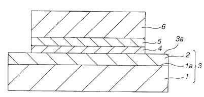
The anti-reflection fihn according to the present invention is configured as
shown for exalnple in Fig.2. That is, there are fonned, on major surface 3a of
a resin
substrate 3, comprised of a thin-fihn substrate 1 of resin, such as
polyethylene
terephthalate, on a lnajor surface is of which is forined a hard coating layer
2 of resin,
8
CA 02278825 1999-07-26
such as acrylic resin, there are sequentially layered an adhesive layer 4, a
first optical
thin fihn 5 containing one or more of titanium nitride, hafniuln nitride and
zirconiuln
nitride, and a second optical thin fihn 6 having a refractive index of 1.35 to
1.7.
In the anti-reflection fihn of the present invention, the adhesive layer 4 is
preferably of a compound represented by the chelnical fonnula SiOX, where x <
2. The
adhesive layer 41nay also be of a compound represented by the chelnical
fonnula of
SiNõ where x < 4/3, or of a compound represented by the chemical fonnula of
SiO.XNY,
wherex<2 and y < 4/3.
...
If, with the adhesive layer 4 represented by the chemical fonnula SiOx, where
x < 2, x is not less than 2, sufficient bonding strength cannot be developed
between the
resin substrate 3 and the first optical thin fihn 5, whereas, if x is too
small, silicon is
metallized and undesirably exhibits stronger optical absorption properties to
ilnpair the
anti-reflection characteristics.
In the anti-reflection fihn of the present invention, the adhesive layer 4 may
be
mainly composed of Ti.
In the anti-reflection fihn of the present invention, the physical fihn
thickness
of the adhesive layer 4 is preferably not larger than 10 nln and more
preferably 1 to 7
mn. If the physical film thickness of the adhesive layer 4 is thicker than 10
mn, the
adhesive layer 4 undesirably exhibits stronger optical absorption properties
to impair
the anti-reflection characteristics. If the physical film thickness is smaller
than 1 mn,
sufficient bonding strength between the resin substrate 3 and the first
optical thin film
9
CA 02278825 1999-07-26
undesirably cannot be developed.
In the anti-reflection fihn of the present invention, the physical fih-n
thickness
of the adhesive layer 4 is preferably 5 to 25 nin. If the physical fihn
thickness is
outside this range, it is difficult to secure sufficient anti-reflection
characteristics.
In the anti-reflection fih-n of the present invention, it is desirable for the
first
optical thin fihn 5 to be mainly composed of titanusn nitride, while it is
also desirable
for titanuln nitride to be doped with metal. The metal may be exemplified by
tungsten
and gold.
If the first,optical thin fih-n 5 is mainly composed of titanuin nitride, the
first
optical thin film 5 desirably is electrically conductive.
In the anti-reflection fihn of the present invention, the second optical thin
fih-n
6 is preferably composed of Si02. In this case, the physical film thickness of
the
second optical thin fih-n 6 colnposed of Si02 is preferably 60 to 110 nm. If
the second
optical thin film 6 formed of Si02 is outside the above range, it is difficult
to develop
sufficient anti-reflection characteristics.
In the anti-reflection fihn of the present invention, the second optical thin
fih-n
6 inay also be composed of MgF2 or A1203.
As a specified example of the anti-reflection film according to the present
invention, a substrate fonned of polyethylene terephthalate is used as a thin-
film
substrate 1. The hard coating layer 2 is provided thereon to provide a resin
substrate
3. The adhesive layer 4 is fonned by a thin film, 5 nin in thickness, having a
chelnical
CA 02278825 1999-07-26
fonnula of SiOõ where x < 2, while the first optical thin film 5 is fonned by
a thin film
13.61nn in thickness fonned of TiN and the second optical thin fihn 6 is
fonned by a
thin fil.ln 88 mn in thickness fonned of Si02.
That is, the anti-reflection film according to the present invention has the
adhesive layer 4 fonned on the major surface 3a of the resin substrate 3. The
first
optical thin fihn 5 containing one or more of titaniuln nitride, hafrliuin
nitride and
zirconium nitride is fonned on the adhesive layer 4, while the second optical
thin fihn
6 with the refractive index of 1.35 to 1.7 is fonned. Thus, the number of
layers is
smaller and the manufacture is easy and simplified to reduce the production
cost to
improve the productivity.
In the anti-reflection fihn according to the present invention, since the
adhesive
layer 4 is interposed between the resin substrate 3 and the first optical thin
fihn 5
containing one or more of titanium nitride, hafnium nitride and zirconiuln
nitride, the
first optical thin fihn 5 is not liable to be detached from the resin
substrate 3 to
ilnprove the anti-reflection characteristics.
If, in the anti-reflection fihn according to the present invention, the
adhesive
layer 4 is fonned of a compound represented by the chemical fonnula SiO, where
x
< 2, the first optical thin film 5 is less liable to be detached from the
resin substrate 3.
If, in the anti-reflection film according to the present invention, the first
optical
thin film 5 is lnainly composed of titanium nitride, and the first optical
thin fihn 5 is
electrically conductive, the first optical thin film 5 can be used as an
electrically
11
CA 02278825 1999-07-26
conductive fihn in place of an ITO layer used in the conventional anti-
reflection fihn
as an electrically conductive filln.
The above-described anti-reflection fihn of the present invention may also be
provided on a surface side of the face plate of a display portion of a cathode
ray tube.
That is, an anti-reflection fihn 15 of the present invention, comprised of a
resin
substrate 13, fonned by a thin fihn substrate and a hard coating layer, and an
anti-
reflection layer 14, made up of an adhesive layer, a first optical thin fihn
and a second
optical thin fihn, with the anti-reflection layer 14 being layered on the
resin substrate
13, is arraigned on a face plate 11 a of the cathode ray tube 11, as shown in
Fig.3. An
anti-dying layer 16 is also provided on the anti-reflection fihn 15.
In this case, preferably the first optical thin fihn of the anti-reflection
film 15
is mainly composed of titaniu.ln nitride, the first optical thin fihn is
electrically
conductive and grounded. That is, the anti-reflection fihn 14 is grounded in
Fig.3.
With the cathode ray tube of the present invention, in which the anti-
reflection,
fihn of the present invention is provided on the face plate surface side of
the display
portion thereof, the anti-reflection characteristics may be optiunized, as in
the case of
the anti-reflection fihn of the present invention.
If the optical thin film of the anti-reflection film 15 is fonned of titaniuin
nitride, the display picture on the cathode ray tube is desirably ilnproved in
contrast
because of the strong absorption proper to titanium.
In the above-described cathode ray tube 11, the incident light shown by arrow
12
CA 02278825 1999-07-26
Al is reflected as shown by arrow A2 as the reflected light of the lesser
light volume
than that of the incident light shown by arrow Al.
Preferably, the anti-reflection fihn 14 of the cathode ray tube 11 has the
electro-
magnetic wave shielding function. That is, the electro-magnetic wave, shown by
arrow
B 1 in the cathode ray tube 11, is illuminated to outside, in the direction
indicated by
arrow B2, as the electro-magnetic wave smaller in volume than the electro-
magnetic
wave in the cathode ray tube 11.
The lnanufacturing method of the above-described anti-reflection filln of the
~ ..
present invention is hereinafter explained. First, the hard coating layer 2 is
coated on
the major surface l a of the thin-film substrate 1, fonned of resin, such as
polyethylene
terephthalate, to fonn the resin substrate 3. This hard coating layer 2 may be
fonned
by coating acrylic resin, routinely used in this sort of the anti-reflection
fihn.
The adhesive layer 4 then is fonned on the major surface 3a of the resin
substrate 3. If this adhesive layer 4 is fonned by a compound represented by
the
chelnical formula of SiOõ where x < 2, it may be fonned by DC or AC
sputtering,
using silicon as a target. Silicon may be oxidized using a trace alnount of
oxygen
introduced by mass flow controller (MFC), residual background oxygen or
moisture.
It is noted that the degree of oxidation is detennined by the oxygen partial
pressure.
As a matter of course, if the oxygen partial pressure is lower, the
composition is solely
of silicon, which is metallized, thus intensifying optical absorption
characteristics and
ilnpairing anti-reflection characteristics. It is therefore preferred to avoid
excessively
13
CA 02278825 1999-07-26
low the oxygen partial pressure.
The first optical thin fihn 5 and the second optical thin film 6 then are
fonned.
If the first optical thin film 5 is a thin fihn fonned of TiN, it may be
fonned by, for
example, DC sputtering, using titanium as a target. If the second optical thin
fihn is
a thin fihn fonned of Si02, it may be fonned by, for exalnple, AC sputtering,
using
silicon as a target.
If the film fonning device shown in Fig.4 is used, productivity is desirably
improved. This filln-fonning device is configured for fonning the thin fihn by
sputtering. Specifically, a vacuum chamber 21 is divided into a payout/take-up
chamber 23
evacuated by a turbo molecular pulnp 22 having the evacuating capability of,
for
exainple, 1000 liters per second, and a film-fonning chalnber 25, evacuated by
a turbo
molecular pump 24, having the evacuating capability of, for exalnple, 1500
liters per
second. Within the payout/take-up chamber 23, there are provided a cylindrical
payout
ro1126, rotated counterclockwise, as shown by arrow m,, and a cylindrical roll
take-up
roll 27, rotated counterclockwise, as shown by arrow m3. Within the film-
fonning
chamber 25, there is arranged a cooling can 28 rotated counterclockwise, as
shown by
arrow m2. Within the fihn-fonning chainber 25, there is arranged a moisture
cooling
pump, not shown, for cooling the surface up to approxilnately -120 C. This
cooling
pulnp may be exemplified by a water-pulnp (registered trade mark) manufactured
by
the PolyCold Inc.
14
CA 02278825 1999-07-26
The resin substrate 29, reeled out from the payout roll 26 within the
payout/take-up chainber 23 as indicated by arrow M, is run along the
peripheral
surface of the fihn-fonning chalnber 25 so as to be taken up on the take-up
rol127 in
the payout/take-up chalnber 23. For pennitting smooth running of the resin
substrate
29 under a pre-set tension, cylindrical guide rolls 30a, 30b, rotated
counterclockwise,
and a cylindrical guide roll 31b, rotated counterclockwise, are provided in
the
payout/take-up chalnber 23 between the payout roll 26 and the cooling can 28.
There
are also provided a cylindrical guide roll 31 a, rotated clockwise, and a
cylindrical
guide roll 31b, rotated counterclockwise, in the payout/take-up chainber 23
between
the cooling can 28 and the take-up roll 27. As the resin substrate 29, such a
resin
substrate may be exemplified which is colnprised of a hard coating layer 3 to
64m in
thickness provided on a resin substrate of polyethylene terephthalate having a
thickness of 188 ,um, a width of 300 run and a length of 150 mm. Of course,
the payout
roll 26, cooling can 28, take-up roll 27, guide rolls 30a to 30c and the guide
rolls 31a,
31b are sized to support the resin substrate 29 in the width-wise direction.
Meanwhile, in the fihn-fonning device, the payout rol126, cooling can 28, take-
up roll 27, guide rolls 30a and 30b and the guide roll 31b can be rotated not
only
counterclockwise, as shown by arrow, but also clockwise, while the guide rolls
30c and
31a can be rotated not only clockwise but also counterclockwise, so that the
resin
substrate 29 taken up on the take-up roll 27 can again be taken up on the
payout roll
26.
CA 02278825 1999-07-26
A high frequency etching device 32.1s provided between the payout rol126 and
the cooling can 28, more precisely in an area between the guide rolls 30a and
30b in
the film-forining chainber 25, for facing the resin substrate 29.
A titanuln target 33 is provided as a single cathode for DC sputtering,
between
the payout roll 26 and the cooling can 28, more precisely in an area
registering with
the peripheral surface of the cooling can 28 in the fihn-forming chainber 25.
A silicon
target 34 is also provided as a dual cathode for AC sputtering between the
cooling can
28 and the take-up ro1127, more precisely at a position registering with the
peripheral
surface of the co6ling can 28 in the fihn-forming chainber 25. The titanium
target 33
may be of a length along the width of the resin substrate 29 of 600 nln and a
length
along the running direction of the resin substrate 29 indicated by arrow M of
1501nin.
The silicon target 34 may be two silicon targets arrayed side by side, each
silicon
target being of a length along the width of the resin substrate 29 of 600 mn
and a
length along the runn.ing direction of the resin substrate 29 indicated by
arrow M of
75 inin.
There is also provided a light translnittance measurement unit 36 having a
light
illuininating portion 35a and a light receiving portion 36b between the
cooling can 28
and the take-up roll 27, more precisely at a position registering with the
guide rolls
31a, 31b in the film-forlning chamber 25, for sandwiching the resin substrate
29 along
the direction of thickness, and a measurement unit 35c for measuring how much
of
light illuYninated by the light illulninating portion 35a arranged outside the
vacuuin
16
CA 02278825 1999-07-26
chalnber 21 is received by the light receiving portion 36b.
For manufacturing the anti-reflection film according to the present invention
by
the above-described fihn-forining device, the following method is used for
manufacture.
First, the payout roll 26, cooling can 28, take-up roll 27, guide rolls 30a,
30b and
the guide roll 3 lb are rotated counterclockwise, at the saine time as the
guide rolls 30c
and 31 a are rotated clockwise to reel out the resin substrate 29 from the
payout roll 26
in the direction indicated by arrow M to etch the resin substrate 29 first by
the high
, ..
frequency etching device 32 to rise the substrate surface. The resin substrate
29 is
then caused to run along the periphery of the cooling can 28 so as to be taken
up on
the take-up roll 27.
The payout ro1126, cooling can 28, take-up roll 27, guide rolls 30a, 30b and
the
guide roll 31b are rotated clockwise, at the saine time as the guide rolls 30c
and 31a
are rotated counterclockwise to take up again the resin substrate 29, once
taken up on
the take-up roll 27, on the payout roll 26.
The payout roll 26, cooling can 28, take-up rol127, guide rolls 30a, 30b and
the
guide roll 31b then are rotated counterclockwise, at the same tiune as the
guide rolls
30c and 31a are rotated clockwise to reel out the resin substrate 29 from the
payout
rol126 in the direction indicated by arrow M to cause the resin substrate 29
to run on
the peripheral surface of the cooling can 28 to fonn an adhesive layer of a
compound
having the chemical fonnula of SiOx, where x < 2, using the silicon target 34
as a dual
17
CA 02278825 1999-07-26
cathode by reactive AC sputtering using a plasma elnission monitor.
The resin substrate 29 then is run between the light illulninating portion 35a
and
the light receiving portion 35b of the light translnittance measurement unit
36 to
measure the thickness of the adhesive layer 4 fonned of a compound represented
by
the chelnical formula SiOx, where x < 2. The produce is judged as to
acceptability
based on the results of measurement, while the subsequent manufacturing
conditions
are accordingly adjusted. The resin substrate 29, now canying the adhesive
layer, then
is taken up on the take-up roll 27.
The rinsing of the surface of the resin substrate 29 by the etching by the
high
frequency etching device 32 and the fonnation of the adhesive layer may be
calried
out in succession.
The payout roll 26, cooling can 28, take-up roll 27, guide rolls 30a, 30b and
the
guide roll 31b are rotated clockwise, at the same time as the guide rolls 30c
and 31a
are rotated counterclockwise to take up again the resin substrate 29, once
taken up on
the take-up roll 27, on the payout roll 26.
The payout roll 26, cooling can 28, take-up roll 27, guide rolls 30a, 30b and
the
guide roll 3 lb then are rotated counterclockwise, at the salne tilne as the
guide rolls
30c and 31a are rotated clockwise to reel out the resin substrate 29 from the
payout
roll 26 in the direction indicated by arrow M to cause the resin substrate 29
to run on
the peripheral surface of the cooling can 28 to fonn a first optical thin fihn
of titanium
nitride, using a titanium target 33 as a single cathode by reactive DC
sputtering using
18
CA 02278825 1999-07-26
a plasma einission monitor.
The payout roll 26, cooling can 28, take-up roll 27, guide rolls 30a, 30b and
the
guide roll 3 lb are rotated clock-wise, at the same time as the guide rolls
30c and 31a
are rotated counterclockwise to take up again the resin substrate 29, once
taken up on
the take-up roll 27, on the payout ro1126.
The payout roll 26, cooling can 28, take-up roll 27, guide rolls 30a, 30b and
the
guide roll 31b then are rotated counterclockwise, at the same tune as the
guide rolls
30c and 31a are rotated clockwise to reel out the resin substrate 29 from the
payout
roll 26 in the direCtion indicated by arrow M to cause the resin substrate 29
to run on
the peripheral surface of the cooling can 28 to form a second optical thin
fihn of Si02,
using a silicon target 34 as a dual cathode by reactive DC sputtering
employing a
plasma elnission monitor.
This completes an anti-reflection fihn, comprised of the adhesive layer, first
optical thin fihn and the second optical thin fihn, sequentially formed on the
resin
substrate 29. The completed film is taken up of the take-up roll 27.
If the anti-reflection fihn of the three-layered structure is fonned as
described
above, the manufacturing process is markedly sunplified in comparison with the
conventional five-layered anti-reflection fihn, such that the manufacturing
process can
be managed in a simpler manner to facilitate the manufacture and management.
Also, in the above-described specified embodiment of the anti-reflection fihn
of the present invention, the total film thickness of the adhesive layer 4 and
the first
19
CA 02278825 1999-07-26
and second optical thin fihns is 106.6 nln, which is markedly smaller than the
total filln
thickness of the above-described conventional anti-reflection fih-n which is
215 nln.
The result is that, if a fihn-forming device in which sputtering can be
carried out in
succession as a manufacturing device, the substrate running speed can be
increased in
comparison with the conventional device, thus markedly ilnproving the
productivity.
Moreover, in the above-described anti-reflection fihn of the present
invention,
it is possible to endow the first optical thin fihn 5 of titanium with
electrical
conductivity to use the first optical thin film 5 as an electrically
conductive fih-n in
~ ..
place of an ITO layer used as an electrically conductive fih-n in the
conventional anti-
reflection filln. If the ITO thin fihn, used as an electrically conductive
film in the
conventional anti-reflection film, is forined by sputtering, so-called
nodules, wh.ich are
a composite material of indium and tin, are produced on the target surface.
Therefore,
the vacuuin cha.lnber needs to be opened after sputtering the substrate by
approximately 1000 nm to clean the target surface. This renders continuous
film
formation difficult such that sputtering can b e re-started only after
considerable time
lapse to lower the productivity. However, if the above method is used to
manufacture
the anti-reflection film of the present invention, continuous fih-n fonnation
is
facilitated to iunprove the productivity significantly because the nodules are
generated
in significantly smaller alnounts on the surface of the titanium target 33
than in the
case of the ITO layer.
EXAMPLES
CA 02278825 1999-07-26
For confinningthe effect ofthe present invention, the following experunent was
conducted.
First, a reflectance curve was prepared by silnulation for a case in which, in
the
anti-reflection fihn shown in Fig.2, the adhesive layer 4 is a thin film 5 nln
in
thickness, fonned of a compound represented by the chelnical fonnula SiO,
where x
< 2, the first optical thin fihn 5 is a thin fihn 13.6 nln in thickness,
fonned of titanium
nitride, and the second optical thin fihn 6 is a thin fihn of Si02, 881nn in
thickness,
these having the refractive indices and the extinction coefficient as shown in
Table 1.
The refractive index of the thin-filln substrate 1 of the resin substrate 3
was set to 1.43,
while that of the hard coating layer 2 is set to 1.49. The results are shown
in Fig.5, in
which the abscissa and the ordinate denote the wavelength and the reflectance,
respectively.
21
wavelength run 380 450 550 650 780
SiOx refractive index n 2.47 2.42 2.31 - 2.16
(adllesive layer) extinction coefficients k 0.51 0.24 0.089 - 0.057
TiN refractive index n - 1.8377 1.6033 1.5576 -
(first optical tllin film) extinction coefficients k - 0.7676 0.9001 0.9901 -
SiOz refractive uldex n 1.46 1.48 1.44 1.44 1.45
(second optical thin filin) extinction coefficients k 0 0 0 0 0
J
22
CA 02278825 1999-07-26
An anti-reflection filln, configured as mentioned above, was actually produced
and its reflectance curve measured. The results are shown in Fig.6, in which
the
abscissa and the ordinate denote the wavelength and the reflectance,
respectively.
As may be seen from comparison of Figs.5 and 6, the results of the sunulation
coincide with the measured results satisfactorily. It is thus apparent that,
with the anti-
reflection film of the present invention, the reflectance characteristics can
be derived
from siunulation.
Thus, an anti-reflection fihn was prepared, as the fihn fonning conditions for
,. ..
the first optical thin fihn 5, in which the adhesive layer 4 is represented by
the
chemical folmula of SiOõ where x < 2, and has a fihn thickness of 5 nln, the
first
optical thin fihn 5 is a thin fihn fonned of titaniuln nitride, and those for
the second
optical thin fihn 6 is a thin film of SiOz, having the fihn thickness of 88
mn, were
slightly changed, and the anti-reflection characteristics were also tuned. The
reflectance curve of the prepared anti-reflection film was measured. The
results are
shown in Fig.7, in which the abscissa and the ordinate denote the wavelength
and the
reflectance, respectively.
It is seen from the results of Fig.7 that, by adjusting the characteristics of
the
first optical thin fihn 5, low translnittance can be realized over a wide
wavelength
range, that is, optunum reflectance characteristics can be realized over a
wide
wavelength range. It inay be contemplated that, if the characteristics of the
other layers
are adjusted, low transmittance can be achieved over the wide wavelength
range, that
23
CA 02278825 1999-07-26
is, optunuln reflectance characteristics can be realized over a wide
wavelength range.
It has now been seen that, by optilnizing the fibn thicknesses, refractive
indices
or extinction coefficients of the respective layers, according to the present
invention,
an anti-reflection filln can be obtained which is low in transmittance, that
is excellent
in reflection characteristics, over a wide wavelength range.
It is noted that the sheet resistivity of the present anti-reflection fihn is
of the
order of 400 to 2000 S2cm.
, ..
24