Note: Descriptions are shown in the official language in which they were submitted.
CA 02278872 1999-07-26
Myer 57
FEED FORWARD AMPLIFIER IIVVIPROVEMENT
INCORPORATING AN AUTOMATIC GAIN AND PHASE CONTROLLER
FIELD OF THE INVENTION
This invention relates to high power linear amplifiers and more particularly
to
control systems employing feed forward to reduce distortion of high power
linear amplifiers.
BACKGROUND OF THE INVENTION
RF linear amplifiers utilize devices that exhibit non-linear characteristics
at
higher power levels whereby signal distortion is introduced. For example, if
more than one carrier
signal is applied to a linear amplifier, its non-linear characteristics cause
an unwanted
multiplicative interaction of the carrier signals being amplified and the
amplifier output contains
intermodulation products or distortion. These intermodulation products cause
interference which
may exceed established transmission standards.
As is well known, intermodulation distortion can be reduced by separating the
distortion component of the amplifier output and feeding forward the
distortion component to
cancel the distortion in the amplifier output signal. FIG. 1 is a simplified
block diagram of a feed
forward circuit 10 disclosed in U.S. Pat. No. 4,885,551. Feed forward circuit
10 receives input
signal S having at least one carrier in a prescribed frequency range. Input
signal S is split into
signals S( 12a) and S( 12b), wherein signals S( 12a) and S( 12b) are signals
representative of the
input signal S. For ease of discussion, numeric references in parenthesis are
used herein to
indicate from which components) a signal was output, and alphanumeric
references in
parenthesis are used herein to indicate that the components) from which the
signal was output
has more than one output. For example, signal S( 12a) would indicate that it
was an output signal
of splitter 12 and that it was one of a multitude of output signals from
sputter 12. If a signal has
more than one reference, the order of the references would indicate the path
of the signal. For
example, signal S( 12a,14) would indicate that it was first an output signal
of the splitter 12 and
then an output signal of an amplifier 14. The output signal of the latter
referenced component
would be a signal representative of the preceding referenced component, e.g.,
signal S( 12a,14) is
a signal representative of the signal S( 12a).
Signal S(12a) is applied to a first or main circuit path having main amplifier
14
which amplifies signal S( 12a) and introduces distortion signal D( 14). Thus,
main amplifier 14
CA 02278872 1999-07-26
Myer 57 2
produces output signal S( 14) comprising signals S( 12a,14) and D( 14). Signal
S( 14) is applied to
directional coupler 18 which directs signals S( 18a) and S( 18b) to delay 22
and cancellation
circuit 20, respectively, wherein signal S( 18a) comprises signals S(
12a,14,18a) and D( 14,18a)
and signal S( 18b) comprises signals S( 12a,14,18b) and D( 14,18b). Signal S
18(a) is delayed by
delay 22 to produce output signal S(22) comprising S( 12a,14,18a,22) and D(
14,18a,22).
Signal S(12b) is applied to a second circuit path where it is delayed by delay
16
to produce output signal S(16) comprising signal S(12b,16). Signal S(12b,16)
is combined with
signal S( 18b) in cancellation circuit 20 to form output signal S(20). In
cancellation circuit 20,
signal S( 12a,14,18b) (via signal S( 18b)) is canceled by signal S( 12b,16).
Thus, signal S(20)
comprises distortion signal D( 14,18b,20). The signal S(20) is applied to
correction amplifier 24
which amplifies signal S(20) and introduces distortion signal D(24). Note that
distortion signal
D(24) is approximately 10,000 times smaller in amplitude than distortion
signal D( 14). Thus,
correction amplifier 24 produces output signal S(24) comprising distortion
signals
D(14,18b,20,24) and D(24). Signal S(24) is combined with signal S(22) in
cancellation circuit 26
to produce output signal S(26). The amplitude and phase of distortion signal
D( 14,18b,20,24)
(via signal S(24)) should be approximately equal to the amplitude and phase of
distortion signal
D( 14,18a,22) (via signal S(22)) such that distortion signals D( 14,18b,20,24)
and D( 14,18a,22)
cancel each other in cancellation circuit 26. Thus, signal S(26) comprises S(
12a, l4,18a,22,26)
and D(24,26). In effect, the amplitude of the distortion signal in output
signal S(26) is being
reduced by substituting a signal representative of distortion signal D( 14)
(i.e., D( 14,18a,22)) with
distortion signal D(24), which has a smaller amplitude.
Ideally, correction amplifier 24 should apply a constant amplitude gain and/or
phase shift to signal S(20) such that the amplitude and phase of distortion
signal D( 14,18b,20,24)
(via signal S(24)) should always be approximately equal to the amplitude and
phase of distortion
signal D( 14,18a,22) for purposes of achieving good cancellation. However, as
conditions change
over time, such as temperature, the amplitude gain and/or phase shift applied
to signal S(20) by
correction amplifier 24 may vary. Such variation may adversely affect the
amount distortion
signal D( 14,18b,20,24) cancels distortion signal D( 14,18a,22). Therefore,
there exists a need to
compensate for changes in conditions to the correction amplifier such that
good cancellation of
distortion signals is maintained.
SUMMARY OF THE INVENTION
CA 02278872 2001-05-22
The present invention is a method and a feed forward circuit incorporating an
automatic gain and phase controller for controlling amplitude gain and phase
shift being applied to
an input signal of an amplifier undergoing changing conditions. The automatic
gain and phase
controller is configured to monitor the amplifier output signals and
manipulate the amplitude and
phase of the amplifier input signal (via a gain and phase adjuster) such that
the amplitude and phase
of the amplifier output signals are substantially identical to those of
previous amplifier output
signals.
In one embodiment, the automatic gain and phase controller controls the
amplitude
and phase of the amplifier output signal by: splitting the amplifier output
signal into output signals
S(a) and S(b); saturating the output signal S(a) to produce a saturated output
signal S(a); adjusting
the amplitude and phase of the output signal S(b) to produce an adjusted
output signal S(b), wherein
the amplitude and phase of the output signal are initially adjusted to
substantially match the
amplitude and phase of an input signal; inputting the adjusted output signal
S(b) to a log detector to
produce a saturated adjusted output signal S(b) and a first signal Slog)
indicating the amplitude of
the adjusted output signal S(b); mixing the saturated adjusted output signal
S(b) with the saturated
output signal S(a) to produce a first mixed signal; inputting the input signal
to the log detector to
produce a saturated input signal and a second signal Slog) indicating the
amplitude of the input
signal; mixing the saturated input signal with the saturated output signal
S(a) to produce a second
mixed signal; determining a phase difference between the adjusted output
signal S(b) and the input
signal using the first and second mixed signals; and determining an amplitude
difference between
the adjusted output signal S(b) and the input signal using the first and
second signals S(log).
In accordance with one aspect of the present invention there is provided a
method
for controlling amplitude and phase of an output signal S comprising the steps
of: splitting the
output signal S(out) into output signals S(a) and S(b); saturating the output
signal S(a) to produce a
saturated output signal S(a); adjusting the amplitude and phase of the output
signal S(b) to produce
an adjusted output signal S(b), wherein the amplitude and phase of the output
signal are initially
adjusted to substantially match the amplitude and phase of an input signal
S(in); inputting the
adjusted output signal S(b) to a log detector to produce a saturated adjusted
output signal S(b) and a
first signal Slog) indicating the amplitude of the adjusted output signal
S(b); mixing the saturated
adjusted output signal S(b) with the saturated output signal S(a) to produce a
first mixed signal;
inputting the input signal S(in) to the log detector to produce a saturated
input signal S(in) and a
second signal Slog) indicating the amplitude of the input signal S(in); mixing
the saturated input
signal S(in) with the saturated output signal S(a) to produce a second mixed
signal; determining a
phase difference between the adjusted output
CA 02278872 2001-05-22
3a
signal S(b) and the input signal S(in) using the first and second mixed
signals; and determining
an amplitude difference between the adjusted output signal S(b) and the input
signal S(in) using
the first and second signals S(log).
In accordance with another aspect of the present invention there is provided a
feed forward circuit comprising: a first directional coupler for receiving an
input signal S and
outputting signals S(a) and S(b) using the input signal S; a main amplifier
for amplifying the
signal S(a) to produce a signal S(main) having a distortion signal D(main) and
an amplified
signal S(a); a second directional coupler for outputting a first signal
S(main) and a second
signal S(main) using the signal S(main); a first delay for delaying the first
signal S(main) to
produce a delayed first signal S(main); a second delay for delaying the signal
S(b) to produce a
delayed signal S(b); a first cancellation circuit for combining the delayed
signal S(b) and the
second signal S(main) to produce a signal S(cancel) having a first signal
representative of the
distortion signal D(main); a third directional coupler for outputting a first
signal S(cancel) and a
second signal S(cancel) using the signal S(cancel); a gain and phase adjuster
for adjusting the
amplitude and phase of the first signal S(cancel) to produce a signal
S(adjust) having a second
signal representative of the distortion signal D(main); a correction amplifier
for amplifying the
signal S(adjust) to produce a signal S(correct) having an amplified second
signal representative
of the distortion signal D(main); a fourth directional coupler for outputting
a first signal
S(correct) and a second signal S(correct) using the signal S(correct); an
automatic gain and
phase controller for controlling the gain and phase adjuster using the first
signal S(correct) and
the second signal S(cancel); and a second cancellation circuit for combining
the second signal
S(correct) and the delayed first signal S(main) to produce a signal S(output)
having a signal
representative of the amplified signal S(a).
Advantageously, the automatic gain and phase controller uses a common log
detector to measure and saturate the amplitudes of amplifier output and input
signals in order to
eliminate variations in amplitude measurement and saturation that might be
present due to the
use of multiple log detectors.
BRIEF DESCRIPTION OF THE DRAWINGS
The features, aspects, and advantages of the present invention will become
better understood with regard to the following description, appended claims,
and accompanying
drawings where:
FIG. 1 depicts a block diagram of a feed forward circuit;
CA 02278872 1999-07-26
Myer 57 4
FIG. 2 depicts a block diagram of a feed forward circuit in accordance with
the present
invention; and
FIG. 3 depicts a block diagram of an automatic gain and phase controller in
accordance
with one embodiment of the present invention.
DETAILED DESCRIPTION
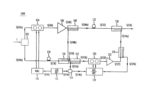
FIG. 2 depicts a block diagram of a feed-forward circuit 100 operative to
amplify
signals across a prescribed frequency range in accordance with the present
invention. Feed
forward circuit 100 includes a splitter 102 for applying composite input
signal S to a first circuit
path and a second circuit path, wherein input signal S comprises one or more
carrier signals S~
across a prescribed band. Sputter 102 receives input signal S and applies
signals S( 102a) and
S( 102b), which are both signals representative of the input signal S to the
first circuit path and the
second circuit path, respectively. For purposes of this application, the term
"splitter" and
"directional coupler" are used interchangeably and shall be construed to
define the same
component.
The first circuit path includes gain and phase adjuster 104, main amplifier
106,
directional coupler 108, delay 132, and cancellation circuit 128. The second
circuit path includes
delay 130, cancellation circuit 110, directional coupler 112, gain and phase
adjuster 120,
correction amplifier 122, directional coupler 124, null circuit 118, log
detector 116, splitter 114
and automatic gain and phase controller 126.
In the first circuit path, the amplitude and/or phase of signal S( 102a) are
adjusted
by gain and phase adjuster 104 (under the control of null circuit 118) to
produce output signal
S( 104) comprising signal S( 102a,104). Specifically, the gain and/or phase of
signal S( 102a) are
adjusted such that a signal representative of it may be subsequently used to
cancel a signal
representative of signal S(102b), as will be described herein. Main amplifier
106 amplifies signal
S( 104) and introduces distortion signal D( 106), thus producing output signal
S( 106) comprising
signal S( 102a,104,106) and distortion signal D( 106).
Directional coupler 108 receives signal S( 106) and applies signal S( 108a)
and
S( 108b) to delay 132 and cancellation circuit 110, respectively, wherein
signal S( 108a) comprises
signal S( 102a,104,106,108a) and distortion signal D( 106,108a), and signal S(
108b) comprises
signal S( 102a,104,106,108b) and distortion signal D( 106,108b). Delay 132
delays signal S( 108a)
without distortion for a time delay T,32 that is set to compensate for the
delay of a signal traveling
through cancellation circuit 110, directional coupler 112, gain and phase
adjuster 120, correction
CA 02278872 1999-07-26
Myer 57
amp 122, and directional coupler 124. Delay 132 produces output signal S(132)
comprising
signal S( 102a,104,106,108a,132) and distortion signal D( 106, l OSa,132).
Cancellation circuit 128
combines signal S(132) with signal S(124a) from directional coupler 124 to
produce output signal
S(128), as will be described herein.
In the second circuit path, delay 130 delays signal S(102b) without distortion
for
a time delay T,3o, wherein the time delay T,3o is set to compensate for the
delay of a signal
traveling through gain and phase adjuster 104, main amplifier 106, and
directional coupler 108.
Delay 130 produces output signal S(130) comprising signal S(102b,130). Signal
S(130) is
combined in cancellation circuit 110 with signal S( 108b) to produce output
signal S( 110). If the
amplitude and/or phase of signal S(102a) is properly adjusted by gain and
phase adjuster 104,
signal S( 102a,104,106,108b) (via signal S( 108b)) should be canceled or
substantially canceled by
signal S(102b,130) (via signal S(130)). Thus, signal S(110) comprises
distortion signal
D(106,108b,110) and difference signal ~S(110), which is the difference between
signals
S( 102b,130) and S( 102a,104,106,108b). For ease of discussion, it will be
assumed that signal
S( 102a,104,106,108b) is canceled or substantially canceled by signal S(
102b,130). Therefore,
difference signal OS( 110) is deemed a negligible component of signal S( I 10)
- that is, signal
S( 110) is viewed hereinafter as comprising only distortion signal D(
106,108b,110) unless
otherwise specified herein.
Signal S( 110) is applied to directional coupler 112, which directs output
signals
S(112a) and S(112b) to splitter 114 and gain and phase adjuster 120,
respectively, wherein signal
S( 112a) comprises distortion signal D( 106,108b,110,112a), and signal S(
112b) comprises
distortion signal D( 106,108b,110,112b). Splitter 114 splits signal S( 112a)
into signals S( 114a)
and S( 114b), wherein signal S( 114x) comprises distortion signal D(
106,108b,110,112a,114a), and
signal S( 114b) comprises distortion signal D( 106,108b,110, I 12a, l l4b).
Signals S( 114a) and
S(114b) are applied to tog detector 116 and automatic gain and phase
controller 126, respectively.
In log detector 116, the amplitude of signal S(114a) is measured to produce an
output signal S(116) which indicates the amplitude of signal S(114a). If
signal
S( 102a,104,106,108b) was not canceled or substantially canceled by signal S(
102b,130), signals
S( 114a) would also include difference signal OS( 110, I 12a,114a) (i.e.,
representative signal of
OS(110)), which typically has a larger amplitude than distortion signal
D( 106,108b,110,112a,114a). The presence of ~S( I I 0,112a,114a) in signal S(
114a) will cause log
detector 116 to output signal S(116) to indicate the amplitude of the larger
amplitude signals that
collectively comprises signal S( 116) - that is, when difference signal OS(
110,112a, 114a) is
present, signal S( 116) will typically indicate the amplitude of difference
signal
CA 02278872 1999-07-26
Myer 57 6
DS( 110,112a,114a). Such indication of difference signal 0S( 110,112a,114a)'s
amplitude is
subsequently used to further minimize the presence of difference signal OS(
110,112a,114a).
Signal S(116) is received by null circuit 118, which uses signal S(116) to
adjust
gain and phase controller 104 such that the difference signal ~S(110) is
minimized in output
signal S(110). The manner is which null circuit 118 uses signal S(116) to
adjust gain and phase
adjuster 104 is well known in the art.
From directional coupler 112, signal S( 112b) is directed to gain and phase
controller 120 where the amplitude and/or phase of signal S( 112b) are
adjusted under the control
of automatic gain and phase controller 126. The amplitude and/or phase of
signal S(112b) is
adjusted such that a signal representative of it may be subsequently used to
cancel distortion
signal D(106,108a,132) (in signal S(132)), as will be described herein.
Gain and phase adjuster 120 outputs signal S( 120) comprising distortion
signal
D( 106,108b,110,112b,120). Correction amplifier 122 amplifies signal S( 120)
and introduces
distortion signal D( 122), thus producing output signal S( 122) comprising
distortion signal
D( 106,108b,110,112b,120,122) and distortion signal D( 122). Signal S( 122) is
applied to
directional coupler 124 which directs signals S(124a) and S(124b) to
cancellation circuit 128 and
automatic gain and phase controller 126, respectively, wherein signal S(124a)
comprises
distortion signals D( 106,108b,110,112b,120,122,124a) and D( 122,124a), and
signal S( 124b)
comprises distortion signals D( 106,108b,110,112b,120,122,124b) and D(
122,124b).
If the gain and phase of distortion signal D( 106,108b,110,112b) (in signal
S(112b)) are properly adjusted by gain and phase controller 120, then
distortion signal
D(106,108a,132) (in signal S(132)) should be canceled or substantially
canceled by distortion
signal D( 106,108b,110,112b,120,122,124a) (in signal S( 124a)). However, the
amount of
amplitude gain and/or phase shift applied to distortion signal D(
106,108b,110,112b,120) by
correction amplifier 122 will vary as conditions, such as temperature, change
over time. This will
affect the amount distortion signal D( 106,108a,132) is canceled by the
distortion signal
D( 106,108b,110,112b,120,122,124a).
The present invention utilizes an automatic gain and phase controller that
compensates for variations in amplitude gain and/or phase shifts being applied
to a signal by an
amplifier under changing conditions. Automatic gain and phase controller 126
uses input signal
S( 112b) (of gain and phase adjuster 120) and output signal S( 122) (of
correction amplifier 122) to
manipulate gain and phase adjuster 120 such that the output signal S(122) of
correction amplifier
122 has little or no variations in amplitude and phase from previous output
signals S(122) under
changing conditions.
CA 02278872 1999-07-26
Myer 57
FIG. 3 depicts a automatic gain and phase controller 200 used in accordance
with
one embodiment of the present invention. Automatic gain and phase controller
200 receives
signal S(124b) and S(114b), which are hereinafter respectively referred to as
S,B and SLO. Signal
SHI is applied to directional coupler 202, which directs signals S(202a) and
S(202b) to limiter 204
and attenuator 230, respectively. In limiter 204, the amplitude of signal
S(202a) is saturated to
produce a signal S(204), which is a signal representative of S(202a) having a
saturated amplitude
or constant peak output (or saturated signal S(202a)). Signal S(204) is
subsequently directed to
mixer 206 where signal S(204) is used as a reference signal for determining
phase differences
between signals S(232) and S,_,o, as will be described herein.
The amplitude of signal S(202b) is adjusted by attenuator 230 to produce
signal
S(230) comprising signal S(202b,230). Signal S(230) is directed to phase
shifter 232, which
adjusts the phase of signal S(230) to produce output signal S(232). In the
initial configuration of
feed forward circuit 100 and automatic gain and phase controller 200,
attenuator 230 and phase
shifter 232 are set to adjust the amplitude and phase of their respective
input signals such that the
amplitude and phase of signal S(232) are identical or substantially identical
to the amplitude and
phase of signal SLO - that is, the amount of adjustment to amplitude and phase
being applied to a
signal by attenuator 230 and phase shifter 232 remains constant after initial
configuration.
Signals S(232) and Sao are provided as inputs to switch 208. Switch 208 has a
first and a second position. In the first position, switch 208 will direct
signal S(232) to log
detector 210. In the second position, switch 208 will direct signal SLO to log
detector 210. Thus,
switch 208 will produce an output signal S(208) comprising either signal
S(232) or signal SLo
depending on the position of switch 208.
Log detector 210 receives signal S(208) and outputs signals S(210a) and
S(210b),
wherein signals S(210a) is a signal representative of signal S(208) with a
saturated amplitude (or
saturated signal S(208)), and signal S(210b) is a signal indicating log of the
amplitude of signal
S(208). Signals S(210a) and S(210b) are directed, respectively, to mixer 206
and switch 220
having a first and a second position. Note that the term log detector, as used
in this application,
shall be construed to define a component operable to saturate the amplitude of
a signal and
measure the log of a signal's amplitude. Similarly, the term limiter shall be
construed to define a
component operable to saturate the amplitude of a signal.
At mixer 206, input signals S(204) and S(210a) are mixed to produce output
signal S(206), which is used to determine the phase difference between signals
S(232) and SLO.
Signal S(206) is subsequently provided to switch 212, which has a first and a
second position.
CA 02278872 1999-07-26
Myer 57 8
From switches 212 and 220, signals S(206) and S(210B) are provided as input
signals to a
plurality of low pass filters 214, 216, 218, 224.
Switches 208, 212 and 220 are collectively controlled by oscillator 222 (e.g.
10
MHz oscillator), which causes switches 208, 212 and 220 to simultaneously
switch between
position 1 and position 2. When switch 208 is in position 1, switch 208 is
directing signal S(232)
to log detector 210. At the same time, switches 212 and 220 are also in
position 1 and directing
signals S(206) and S(210b) to low pass filters 214 and 218, respectively. By
contrast, when
switch 208 is in position 2, switch 208 is directing signal SLO to log
detector 210. At the same
time, switches 212 and 220 are also in position 2 and directing signals S(206)
and S(210b) to low
pass filters 216 and 224, respectively.
Specifically, when switch 208 is in position 1, mixer 206 is outputting a
signal
S(206) comprising a mixture of reference signal S(204) (which, as mentioned
earlier, is a signal
representative of S,a with a saturated amplitude) and signal S(210a) that is
representative of Sm
with a saturated amplitude and adjusted amplitude and phase. Such signals
S(210a) and S(206)
are also referred to herein as first signal S(210a) and first signal S(206).
By contrast, when
switch 208 is in position 2, mixer 206 is outputting a signal S(206)
comprising a mixture of
reference signal S(204) and signal S(210a) that is representative of signal
SLO with a saturated
amplitude. Such signals S(210a) and S(206) are also referred to herein as
second signal S(210a)
and second signal S(206). Note that first and second signals S(210a) are mixed
with the same
reference signal S(204) allowing for an accurate measurement of phase
difference between
signals S(232) and SLO, as will be described herein.
First signal S(206) and second signal S(206) are directed by switch 212 to low
pass filters 214 and 216, respectively. Low pass filters 214 and 216 produce
output signals
S(214) and S(216), respectively, which are directed to differential amplifier
226. Differential
amplifier 226 produces an output signal S(226) which indicates the phase
difference between
signals S(232) and SLO. Such signal S(226) is subsequently used to adaptively
control gain and
phase adjuster 120 such that the phase of output signal S( 122) matches or
substantially matches
the phase of the previous output signals S( 122).
When switch 208 is in position 1, log detector 210 is outputting a signal
S(210b)
indicating the amplitude of signal S(232). Such signal S(210b) is also
referred to herein as first
signal S(210b). By contrast, when switch 208 is in position 2, log detector
210 is outputting a
signal S(210b) indicating the amplitude of signal SLO. Such signal S(210b) is
also referred to
herein as second signal S(210b).
CA 02278872 1999-07-26
Myer 57 9
First and second signals S(210b) are directed to low pass filters 218 and 224
to
produce output signals S(218) and S(224), which are subsequently directed to
differential
amplifier 228, respectively. Differential amplifier 228 produces an output
signal S(228) which
indicates the difference in amplitude between signals S(232) and SLO. Such
signal S(228) is
subsequently used to adaptively control gain and phase adjuster 120 such that
the amplitude of
output signal S( 122) matches or substantially matches the amplitude of
previous output signals
S( 122).
Advantageously, the present invention automatic gain and phase controller use
of
a common log detector 210 to measure and saturate the amplitudes of input
signals S(232) and
SLO eliminates variations in amplitude measurement and saturation that might
be present due to
the use of multiple log detectors. Similarly, the present invention automatic
gain and phase
controller use of a same reference signal S(204) to mix with first and second
signals S(210a)
eliminates variations in phase measurements.
Although the present invention has been described in considerable detail with
reference to certain embodiments, other versions are possible. For example,
signals S(232) and
SLO may be inputted to a limiter (instead of the log detector) for purposes of
saturating the
amplitudes of the signals (before the signals are inputted to the mixer).
Therefore, the spirit and
scope of the present invention should not be limited to the description of the
embodiments
contained herein.