Note: Descriptions are shown in the official language in which they were submitted.
CA 02278973 1999-10-21
-1-
ID1065 CA
A FULLY INTEGRATED LONG TIME CONSTANT
INTEGRATOR CIRCUIT
Field of the Invention
The present invention relates to a fully integrated long time constant
integrator circuit which finds application in long time constant feedback loop
arrangements such as control circuits in optical receivers.
Background to the Invention
The ever incrE~asing demands for high capacity communications
systems has seen the wide spread employment of optical fibre networks
across the world. A fundamental component for such systems is a means
of converting opticall pulses comprising a digital bit stream into electrical
signals. This component of such a system is commonly known as an
optical receiver.
The operational requirements of such a receiver are very demanding.
The receiver is required to exhibit a very low noise characteristic, such that
it is capable of detecting very low levels of optical input in systems
employing maximurn optical fibre lengths, thus requiring high gain
amplification for ma:~cimum sensitivity, but is conversely required to cope
with high levels of optical input in systems employing short fibre lengths,
thus requiring low Main amplification. As such, the optical receiver is
required to have a wide dynamic range which can only be practically
achieved with somE~ form of automatic gain control (AGC). A typical
integrated circuit (IC) optical receiver 10 is illustrated in block schematic
form in Fig 1. This comprises an IC (denoted by broken line 12) including a
transimpedance amplifier stage (denoted by broken line 14) with an
integrator in a control loop providing AGC.
CA 02278973 1999-10-21
-2-
As illustrated by' Fig 1, optical input power OP,N is converted into an
electrical current I,N by a PIN diode photodetector 16. This current I,N is
applied as an input to the IC optical receiver 10. The input current I,N is
amplified by a transimpedance amplifier (Tz Amp) 18 which converts the
input current I,N into an amplified voltage output signal VouT. To meet the
requirement of wide dynamic range, the output voltage VouT of the Tz Amp
18 which is in the form of a broadband data signal and may be considered
as an ac, multi-frequency signal, is rectified or peak detected by a
rectifier/peak detector 20 to provide a do signal level VREC for comparison
with a pre-determinE:d do reference voltage VREF. The difference between
the rectified/peak detected output voltage VREC and the reference voltage
VREF is considered as an error signal which is amplified and integrated by a
Miller Integrator 22 to provide a control signal VcoNTRO~. A Miller Integrator
is
a well known form of integrator incorporating an active device such as a
transistor amplifier. 'The Miller Integrator 22 is required to have a high
gain,
in order to ensure i:hat the error signal approaches zero (ie in order to
ensure that the difference between the rectified/peak detected output
voltage VREC and the reference voltage VReF becomes zero) by means of
controlling the gain of the Tz Amp by varying the impedance of a feedback
resistor 24.
If the rectified/peak detected output voltage VREC is smaller than the do
reference voltage VF~EF, then the Tz Amp 18 must operate at high gain to
provide high sensiti~rity of the optical receiver. When the rectified/peak
detected output voltage VREC becomes just greater than the do reference
voltage VREF, then the on-set of AGC occurs and continues whilst the input
channel I,N increases;. When the feedback resistor 24 is at a minimum the
Tz Amp is operating at very low gain and approaches an overload
condition.
In addition, the' Miller Integrator is required to have a long time
constant (Tp) so that the effect of the AGC action of the control loop does
not compromise data embedded in the voltage output signal VouT of the Tz
Amp.
CA 02278973 1999-10-21
-3-
The requirements for the time constant Tp of the Miller integrator can
be better understood with reference to Fig 2 which identifies the
fundamental gain stages of the typical optical receiver of Fig 1.
To understand the effects of the Miller Integrator time constant Tp,
each gain block of the optical receiver 10 must be considered. For a first
order approximation, the Tz Amp gain of the optical receiver 10 is
proportional to VDUT'/IIN and can be considered as the value Rf of the
feedback resistor 24. This assumes that the Tz Amp gain is constant for all
frequencies up to an upper -3dB point. This assumption is only true if the
AGC is not operating which is often the case at low optical input levels.
Once the AGC begiins to operate to prevent the output signal Vo~T from
increasing further, this has a significant effect on the Tz Amp gain. Using
standard feedback control theory, the presence of a pole in the control loop
feedback path (ie Tp~ of the Miller Integrator) presents a zero in the forward
Tz Amp gain path, reduced by a factor of the loop gain. To illustrate the
above, consider the loop gain of the optical receiver as :-
Loop Gain = Tz,,.A~.A~/Rf
where Tzo == Open loop gain of the Tz Amp
Rf = Value of the feedback resistor
A~ = Rectifier gain
Ao = Open loop gain of the Miller Integrator
The forward closed loop transimpedance gain of the Tz Amp is given
by: Tz~~==( 1 +sTz). Rf
where S = t_aplace operator
and Tz = Tp/(Loop Gain)
.'. Tz = Tp. Rf/(Tzo.A~.Ao)
Consequently, the time constant Tz in the forward Tz Amp gain path is
greatly reduced by the loop gain of the control circuit. In the typical
arrangement, the ~Ailler Integrator pole position (ie Tp of the Miller
CA 02278973 1999-10-21
-4-
Integrator) is such that it results in a transmission zero in the MHz region.
This can have the undesirable effect of generating pattern dependant fitter
in the broadband data stream.
In a typical scenario, for a 155Mbit/sec data stream, the transmission
zero should be at 25KHz or below to prevent fitter in the broadband data
stream, representing a time constant Tz = 6.36~secs. Typically, Tzo = 4M ,
A~ = 2, Ao = 100 and Rf = 50K . Consequently, the loop gain is 16000(or
84.1dB). This requires a very long, relatively speaking, Miller Integrator
time constant Tp of approximately 0.1secs.
Using present k>ipolar IC technology, the maximum practicable size of
resistors than can be manufactured "on chip" are in the MS2 region. For
example, if a 1.5M resistor is fabricated on chip, the required value of
capacitor to provide a 25KHz high pass cut-off needs to be in the order of
67nF. However, present bipolar IC technology allows a maximum
practicable value of capacitors in the region of tens to hundreds of pF to be
formed on chip. Therefore, it can be seen that to achieve the necessary
high pass cut-off frequency of 25KHz would require connection of a large
size discrete component capacitor to the optical receiver integrated circuit.
This normally comprises a lumped silicon device which is mounted on pads
on the silicon substrate containing the integrator IC. The optical receiver IC
is normally containE~d in a DIL package which is hermetically sealed.
Experience has shown that it is the connections of the discrete component
capacitor which provide the most likely points of failure of the device under
test. Failed devices are normally discarded, it being extremely difficult and
expensive to recover any of the constituent parts of the device for reuse. A
known alternative i~; to connect a combination of discrete resistor and
capacitor components to the optical receiver IC but this is equally
undesirable for the same reasons as aforesaid.
It is also known to fabricate IC transimpedance amplifiers using
BiCMOS technology. In such a case, a Field Effect Transistor (FET) can be
used to provide very low current leakage of an on-chip capacitor which has
been charged from the peak detection circuit thus providing the necessary
long time constant. This technology allows a fully integrated IC optical
CA 02278973 1999-10-21
-5-
receiver to be provided but at a higher cost than one provided using bipolar
technology.
Objects of the Invention
The invention seeks to provide a long time constant IC integrator
without requiring external large value capacitor and/or resistor components.
The invention also seeks to provide a long time constant bipolar IC
integrator.
The invention further seeks to provide a fully integrated circuit
transimpedance amplifier for an optical receiver.
The invention further seeks to provide a transimpedance amplifier for
an optical receiver which obviates some of the problems encountered with
known IC transimpectance amplifiers.
Summay of the Invention
The present invention provides an integrated circuit (IC) integrator
consisting of an input attenuation stage followed by an operational amplifier
stage configured as a Miller Integrator. A resistive element couples the
output of the attenuation stage to the input of the op-amp stage. The op
amp stage has a 'feedback loop coupling its output to its input, said
feedback loop including a capacitive element. The capacitive and resistive
elements define between them a fundamental time constant CR for the
circuit. However, thE~ effect of the attenuation stage is to multiply the
effect
of the resistive element thereby enhancing the time constant of the circuit.
The integrated circuit integrator is formed using a bipolar process using only
npn devices although other bipolar technology is applicable. The integrator
circuit in accordance with the invention has the potential to provide an
enhanced circuit time constant which is in the order of 1000 times greater
than the fundamental time constant. This is the consequence of two
effects. The fundamental time constant is increased on the one hand by
the gain provided by the op-amp stage and on the other hand is enhanced
as a result of the attenuation achieved in the attenuation stage. In the
preferred embodiment, the attenuation stage comprises a transconductant
stage.
CA 02278973 1999-10-21
-6-
Brief Description of the Drawings
For a better understanding of the invention and to show how the same
may be carried into effect, there will now be described by way of example
S only a preferred embodiment with reference to the accompanying drawings
of which:
Figure 1 is a block schematic diagram of a typical IC optical receiver
with automatic gain control (AGC);
Figure 2 is a block schematic diagram identifying the fundamental gain
stages of the optical receiver of figure 1;
Figure 3 is a block schematic diagram of a discrete component
integrator circuit as dlisclosed in applicant's co-pending US application
serial
no. US 08/729,099 illustrating its relationship to a fully integrated circuit
integrator in accordance with the invention;
Figure 4 is a block schematic diagram of a fully integrated circuit
integrator in accordance with the invention; and
Figure 5 is a circuit diagram for a fully integrated circuit integrator in
accordance with the invention.
Description of the Invention
Applicant's co-pending application, US serial no. 08/729,099 (Visocchi)
the contents of which are incorporated herein, discloses a "modified" Miller
Integrator circuit as schematically illustrated in fig 3 which has the
potential
to provide an enhanced time constant. The Miller Integrator circuit 30 as
disclosed in US serial no. 08/729,099 has a discrete component form
comprising a combination of operational amplifiers (op-amps) and other
discrete circuit components. Devices such as op-amps are readily available
as standard "plug-in" components.
The circuit comprises first and second op-amps A1, A2. The output of
the first op-amp A1 is connected by first and second resistors R1, R2 to
ground and via the first and a third resistor R1, R3 to an inverting input of
the second op-amp ,A2. The first op-amp A1 has a feedback connection
between its output and its inverting input. The second op-amp A2 is
configured as a Miller Integrator. The circuit is arranged with a feedback
from the output actirn~ on the inverting input of the second op-amp A2. The
feedback incorporates a capacitor C. The output of the second op-amp A2
CA 02278973 1999-10-21
-7-
is connected by a fourth resistor R4 to the non-inverting input of the first
op-
amp A1. The circuit includes a fifth resistor R5 as an input resistor.
In this circuit v°_ _ A°-
V,N 1 + .STp
1+Ao
and Tp = C RC A
R2
where A = -
R1 + R2 '
R1R2
R=R3+
R1+R2
and Ao = R4 / RS
The effect of placing an attenuation network formed by R1 & R2 within
the feedback path of the two op-amps, multiplies the effect of the source
resistance which is modelled by R. If the parallel combination of R1 & R2 is
small in comparison to R3, then R ~ R3. The effect on R is multiplied by (1
+ Ao) but with the addition of only two resistors providing an attenuated
signal, the multiplication is enhanced to (1+Ao)/A. This allows the size of
discrete components to be maintained at a practicable size whilst still
achieving a relatively long time constant.
This effect is also beneficial in an application such as a control loop,
since closed loop zero is divided by the gain of the integrator, the modified
Miller Integrator gain multiplies the time constant by (1+Ao), thus the zero
Tz becomes:-
CR(1+Ao)Rf
Tz =
TzoAoA,~4
This can be further reduced to:-
CA 02278973 1999-10-21
_8_
CRRf
Tz
TZoArA
Since the effect: of the high gain (ie ~ 40dB) of the Miller Integrator has
effectively been eliminated from defining the transmission zero Tz, this has
greatly reduced the required value of the fundamental CR time constant
required. Thus, using in the IC example described above, where Tzo =
4M , Ar = 2, Rf = 50K and if A is designed to give an attenuation of 0.086
(ie ~ -21.34dB) then if a 1.5M resistor is fabricated on chip, the required
minimum capacitor i:o provide a 25KHz high pass cut-off would be 58pF.
This represents a 1,172 reduction in the size of capacitor required. Hence
there is no need for <~ny external capacitive or resistive components.
The design of such a long time constant integrator (LTI) in an
integrated circuit form using bipolar technology would not use an op-amp
configured as a unity gain amplifier or form an attenuation stage with a
resistive divider. In addition, to ensure maximum power supply rejection
and reduction of common mode noise, the LTI would be configured in a fully
differential manner. The relationship between the discrete component form
of the LTI and a fully integrated circuit form of the LTI is illustrated by
means of dotted lines 32, 34 in Fig 3. Dotted line 32 denotes that part of
the discrete circuit which can more effectively be achieved as a
transconductance stage in IC form. Dotted line 34 denotes that part of the
discrete circuit that can be achieved in a standard IC op-amp configuration.
The transformation to the fully integrated circuit form is further illustrated
by
Fig 4 in which it can be seen that the circuit 40 comprises an input
transconductance stage 42 feeding an amplifier stage 44 and including a
closed loop feedback. The amplifier stage has a feedback including a
capacitor C between its input and output. Other circuit elements equivalent
in operation to those of the discrete circuit are denoted by the same
identifiers.
Figure 5 is a circuit diagram for a preferred embodiment of the LTI.
The component values identified in figure 5 are given by way of example
only and should not be taken as limitative of the scope of the invention.
CA 02278973 1999-10-21
_g_
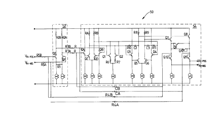
As illustrated by Fig 5, the LTI 50 is formed by two main parts, a
transconductance input stage 52 followed by an operational amplifier (op-
amp) stage 54. The closed loop voltage gain of the LTI is determined by
the feedback resistors R4A, R4B and the input resistors RSA, RSB. The
fundamental time constant is formed by the resistors R3A, R3B, connected
between the output of the transconductance stage to the input of the op-
amp stage, and the capacitors CA, CB connected between the output and
input of the op-amp. The attenuation network required for the time constant
multiplication is formed by the (low) voltage gain of the transconductance
stage, determined by R2A, R2B and R1 (A~2R2/R1~0.086). The
transconductance stage is provided by QE, QF, R1, R2A and R2B.
The op-amp stage has an active gain stage formed by QA, QB, Q~, Qp,
RA and Rg and is required to have a high input impedance in order that the
time constant resistance formed by R3A, R3B is not lowered. In addition,
low input current (base currents) must be maintained to ensure low voltage
drop across R3A, R3B which are each made 1.5M in value. The op-amp
is also required to provide high open loop gain in order that there is
sufficient gain remaining after the attenuation stage that a closed loop gain
of about 40dB can be maintained. This can be achieved by the use of pnp
transistors or in the case of the circuit of Fig 5 by the use of an active
positive feedback to enhance open loop gain. The active positive feedback
is formed by the network of Q1, Q2 and R6, R7. The output of the active
gain stage is followed by a secondary gain stage configured as a buffered
long tail pair formed by Q3, Q4, Q5, Q6, R8 and R9. The resistive capacitor
network formed by R10, C2 and R11, C3 is used for stability. The output
drive of the op-amp is an emitter follower stage formed by Q7, Q8. The
diodes formed by Q9, Q10 ensure that the output voltage swing is restricted
to ~ vbe. The diodes formed by Q11, Q12 provide the required common
mode voltage to bias the next stage. It is important to note that the design
of the op-amp stage of the LTI is important for the correct operation of the
circuit but does not: in itself constitute the novel aspect of the present
invention. Other op-amp designs would be equally applicable as would be
apparent to a skilled man.
The LTI of Fig 5 provides a voltage gain of 40dB and an effective time
constant of 99.5mS (ie a low pass cut-off of 1.6Hz) white only employing a
CA 02278973 1999-10-21
-10-
maximum resistor of 1.5M and a maximum on-chip capacitor of 58pF,
which ordinarily would provide a fundamental time constant of 87~S.
Consequently, the circuit design of the present invention is such that a 1144
times increase in the effective time constant over that which would seem
possible with a fully integrated on-chip circuit using present bipolar
technology. By using a high performance bipolar technology and providing
a very long time constant integrator, both high performance and low cost
optical receivers can be achieved.
It will be understood by a skilled man that the techniques of using
Miller Integrator stages and attenuator stages to achieve enhanced time
constants can be employed in other IC technologies such as BiCMOS,
GaAsFET for example.