Note: Descriptions are shown in the official language in which they were submitted.
CA 02279031 1999-07-29
SWEEP PILOT TECHNIQUE FOR A CONTROL SYSTEM THAT REDUCES
DISTORTION PRODUCED BY ELECTRICAL CIRCUITS
Background of the Invention
Field of the Invention
The present invention is directed to a control system comprising an electrical
circuit that uses a pilot signal to substantially cancel distortion produced
by the electrical
circuit and more particularly to a technique of traversing or sweeping the
pilot signal
to across the band of operation of the electrical circuit.
Description of the Related Art
Electrical signals when applied to electrical circuits are often distorted as
a result
of being processed by the circuits. Also electrical circuits generate signals
for various
useful purposes. The distortion comprises any undesired signals produced by
the
electrical circuits which are added to or are somehow combined with the
applied or
generated signals. A well known technique for substantially canceling
distortion
produced by an electrical circuit uses a control system coupled to the
electrical circuit to
2o which a pilot signal is applied. The applied pilot signal is detected by
the control system.
The applied pilot signal can have a single spectral component (i.e., one
frequency) of a
certain amplitude or the applied pilot signal can comprise a plurality of
spectral
components of various amplitudes. Typically, the applied pilot signal has an
amplitude
that is at least 60 dB lower than signals applied to or generated by the
electrical circuit.
The control system obtains information from the detected pilot signal and uses
that
information to substantially cancel the distortion produced by the electrical
circuit.
A control system comprises at least one circuit which uses external signals or
signals generated by the at least one circuit to process signals applied to
the at least one
3o circuit. A particular implementation of the technique discussed above is
shown in FIG. 1.
FIG. 1 depicts a control system, comprising two feed forward loops (loop l and
loop 2)
and detection circuit 132. A pilot signal is applied to electrical circuit 108
via coupler
CA 02279031 1999-07-29
2
105. Electrical circuit 108 can be any electrical and/or electronic (e.g.,
Radio Frequency
(RF) linear amplifier, power amplifier) circuit. Loop 1 comprises coupler 105,
Gain &
Phase circuit 104, splitter 102 and delay circuit 126. Coupler 105 is
typically a device
which combines two or more input signals and allows access to all or a portion
of the
combined signal. A coupler is also used to obtain a portion of a signal
appearing at its
input and output. Gain & Phase circuit 104 is typically a circuit which
modifies the
amplitude and phase of signals applied to its input based on the values of
control signals
applied to its control inputs (not shown). Splitter 102 is a circuit with one
input and at
least two outputs where a signal applied to the input is substantially
replicated at the
outputs. Delay circuit 126 is typically a circuit which applies a certain
amount of delay
to a signal applied to its input.
When a signal is applied to the input of the control system (i.e., to sputter
102),
the distortion experienced by the applied signal due to electrical circuit 108
is isolated at
point A (i.e., path 123). In particular, an input signal is applied to
splitter 102. Sputter
102 substantially replicates the input signal on paths 103 and 127. In path
103 the input
signal is applied to Gain & Phase circuit 104, coupler 105 and electrical
circuit 108. In
path 127, the input signal is delayed by delay circuit 126 and then fed to
cancellation
circuit 124 via path 125. Although not shown, it will be readily understood to
those
2o skilled in the art that the amplitude and phase of the input signal on path
125 can be
detected (using well known detection circuitry) and converted to control
signals that are
applied to the control inputs (not shown) of Gain and Phase circuit 104. Using
coupler
112, a portion of the input signal (plus any distortion produced by electrical
circuit 108)
appearing at the output of electrical circuit 108 is fed to cancellation
circuit 124 via path
113. Cancellation circuit 124 can be implemented as a combiner circuit which
has at
least two inputs and one output. A combiner circuit combines signals applied
to its inputs
and transfers the combined signal to its output. Gain and Phase circuit 104 is
adjusted
such that the amplitude and phase of the input signal on path 113 are modified
resulting
in that signal being substantially 180° out of phase (+/- 1 ° )
and relatively the same
3o amplitude (i.e., substantially the inverse) with the input signal on path
125 such that when
the two signals are combined by cancellation circuit 124 they substantially
cancel each
CA 02279031 1999-07-29
3
other leaving the distortion (produced by electrical circuit 108) at point A
(path 123).
Thus Loop 1 is designed to isolate the distortion produced by electrical
circuit 108.
Loop 2, which comprises delay circuit 114, coupler 116, Gain & Phase circuit
122, and amplifier 120, is designed to use information obtained by Detection
circuit 132
from a pilot signal applied to electrical circuit 108 to substantially cancel
the distortion
produced by electrical circuit 108. In particular, a pilot signal is applied
to electrical
circuit 108 via coupler 105. The pilot signal (processed by electrical circuit
108) appears
on path 115 and at the output of coupler 116, i.e., on path 117. The pilot
signal also
1o appears at point A on path 123 after having propagated through path 113 via
coupler 112.
A portion of the pilot signal processed by electrical circuit 108 is fed to
detection circuit
132 via coupler 130 and path 128. Detection circuit 132 comprises well known
circuits
(e.g., Log detector/amplifier, Sample & Hold circuit, Null circuit) to detect
signal -
characteristics (e.g., amplitude) of the pilot signal. Detection circuit 132
detects the
amplitude of the input and uses this information to generate control signals
on path 131 to
cause Gain & Phase circuit 122 to modify the pilot signal. The pilot signal at
point A is
modified such that the pilot signal appearing on path 118 is substantially the
inverse
(relatively same amplitude, 180° out of phase, +/- 1 ° ) of the
pilot signal appearing on
path 115. Amplifier 120 provides additional gain to the output of Gain & Phase
circuit
122. The additional gain is calculated such that the signal appearing on path
118 has an
amplitude substantially equal to the amplitude of the signal on path 115.
Delay circuit
114 is designed such that the two pilot signals arrive at coupler 116 at
substantially the
same moment; that is, the two pilot signals are substantially synchronized
(aligned in
time) to each other. When the two pilot signals are combined by coupler 116
they cancel
each other.
Detection circuit 132 now has the information that allows Gain & Phase circuit
122 to modify distortion appearing at point A and thus cancel distortion
appearing at the
output of electrical circuit 108. When an input signal is applied to the
control system,
3o any distortion produced by electrical circuit 108 is isolated at point A
(on path 123) as
discussed above. The signal on path 115 is the input signal (processed by
electrical
CA 02279031 1999-07-29
4
circuit 108) plus any distortion produced by electrical circuit 108. The
distortion at point
A is modified by Gain and Phase circuit 122 based on the information (i.e.,
signal
characteristics) obtained from the previously applied pilot signal so that the
distortion on
path 129 is substantially the inverse of the distortion on path 115. The
distortions on path
115 and path 118 are combined at coupler 116 causing the distortions to
substantially
cancel each other resulting in an output signal that is substantially free of
distortion.
Electrical circuit 108 has a bandwidth that defines a frequency band of
operation.
It is desirable that the pilot signal be spectrally located substantially in
the middle of the
1o frequency band of operation of electrical circuit 108. However, placing the
pilot signal
anywhere in the band of operation of electrical circuit 108 causes
interference to occur
between the input signal and the pilot signal adding more distortion to the
input signal.
The interference is any interaction between the pilot signal and an applied or
generated
signal that adversely affects one or more characteristic (e.g., amplitude,
frequency, phase)
of the applied or generated signal and/or the pilot signal. Thus, interference
not only
distorts any signal that is applied or generated by the electrical circuit,
but also affects the
pilot signal. As discussed above, the pilot signal is typically 60 dB lower
than the applied
or generated signals and thus would be interfered with by such signals. A
distorted pilot
signal provides inaccurate information about the distortion and thus the very
purpose of
2o such a pilot signal is defeated. Also, even when the pilot signal is
located in the middle
of the frequency band of operation, it does not experience the distortions
located in other
parts (e.g., lower band or upper band) of the frequency band of operation.
What is
therefore needed is to use a pilot signal that obtains information about the
entire
frequency band of operation of the electrical circuit and does so without
interfering with
any signals applied to or generated by the electrical circuit.
Summary of the Invention
The present invention is a control system comprising an electrical circuit
that
3o produces distortion where the electrical circuit has a frequency band of
operation. A
carrier signal modulated by a pilot signal is applied to the electrical
circuit and is
CA 02279031 1999-07-29
traversed across at least a portion of the frequency band of operation of the
electrical
circuit. As the pilot modulated carrier signal traverses the at least portion
of the
frequency band of operation of the electrical circuit information about the
distortion
produced by the electrical circuit is selectively obtained from the pilot
signal.
Information about the distortion is not obtained during periods of time when
the control
system has determined that there is interference between the traversing pilot
modulated
carrier signal and signals applied to or created by the electrical circuit.
The information
obtained is used by the control system to substantially cancel the distortion
produced by
the electrical circuit.
1o
The control system of the present invention also comprises a first feed
forward
loop and a second feed forward loop coupled to the electrical circuit. The
control system
of the present invention further comprises a Carrier circuit coupled to a
Single Side Band
(SSB) modulator which is coupled to the electrical circuit. The control system
of the
15 present invention still further comprises a Detection circuit coupled to
the carrier circuit
and the second feed forward loop. The Carrier circuit is configured to
generate a
traversable carrier signal. The SSB modulator is configured to generate a
single side
band pilot signal and to modulate the carrier with the single side band pilot.
The Carrier
circuit is further configured to cause the pilot modulated carrier signal to
traverse at least
2o a portion of the frequency band of operation of the electrical circuit
without interference
from any signal applied to or generated by the electrical circuit. As the
pilot modulated
carrier signal traverses the at least portion of the frequency band of
operation, the
Detection circuit selectively obtains information about the distortion
produced by the
electrical circuit and provides the information to the second feed forward
loop. The first
25 feed forward loop is configured to isolate the distortion produced by the
electrical circuit.
The second feed forward loop is configured to use the information obtained by
the
Detection circuit to substantially cancel the distortion produced by the
electrical circuit.
CA 02279031 1999-07-29
6
Brief Description of the Drawings
FIG. 1 depicts a control system comprising two feed forward loops and
detection
circuitry;
FIG. 2 depicts a control system of the present invention;
FIG. 3 depicts the frequency response of the electrical circuit of the control
system of the present invention, a pilot modulated carrier and the direction
in which the
pilot modulated carrier signal traverses.
1o Detailed Description
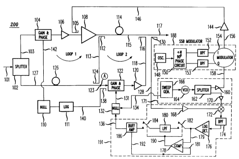
Referring to FIG. 2, there is shown a control system of the present invention
comprising electrical circuit 108 coupled to a first feed forward loop (i.e.,
loop 1) and a
second feed forward loop (i.e., loop 2). The control system of the present
invention
further comprises Carrier circuit 171 coupled to Single Side Band (SSB)
modulator 188
and to Detection circuit 191. Electrical circuit 108 produces distortion which
is isolated
at point A by loop 1. Loop 2 uses information obtained from Detection circuit
191 to
cancel the distortion produced by electrical circuit 108. The information
obtained by
Detection circuit 191 is gleaned from a pilot modulated carrier signal applied
to electrical
2o circuit 108 (via path 146 and coupler 105) with the use of carrier circuit
171 and Single
Side Band modulator 188. Carrier circuit 171 and SSB modulator 188 cause the
pilot
modulated Garner signal to traverse the frequency band of operation of
electrical circuit
108. As the pilot modulated carrier signal traverses the frequency band of
operation of
electrical circuit 108, Detection circuit 191 obtains information from the
pilot only when
Detection circuit 191 determines that there is substantially no interference
between the
traversing pilot modulated carrier signal and any signal applied to or
generated by
electrical circuit 108.
Referring to FIG. 3, there is shown a frequency response (300) of electrical
circuit
108 with a spectral component (306) representing the pilot modulated carrier
signal. The
frequency response is a chart or graph showing how a particular characteristic
(e.g.,
CA 02279031 1999-07-29
7
amplitude, phase) of an electrical circuit corresponds with frequency. The
frequency
band of operation is a range of frequencies within which electrical circuit
108 processes
and/or generates signals. The boundaries of the frequency band of operation
are defined
by lower frequency f L and upper frequency f ~ . Frequencies f L and f ~
correspond to
the points (302, 304) at which the frequency response is 3 dB below its
maximum
amplitude response (0 dB). Typically the bandwidth of a circuit is defined by
the
frequencies that correspond to its 3 dB points. The frequency band of
operation need not
be the bandwidth. Pilot modulated Garner signal 306 initially starts at a
location (f, )
outside the frequency band of operation and then traverses the frequency band
of
to operation or at least a portion of the band in the direction shown by arrow
308. It should
be noted that the particular frequency response shown is for illustrative
purposes only and
that electrical circuit 108 is not limited to frequency response 300. Also,
pilot modulated
carrier signal 306 need not initially start at a location (fl ) proximate to
fL . Pilot
modulated carrier signal 306 can, for example, start at a location (frequency
fF )
proximate to fU and traverse the frequency band of operation in a direction
opposite that
of arrow 308.
Referring again to FIG. 2, Carrier circuit 171 comprises Sweep Generator 166
coupled to Voltage Controlled Oscillator (VCO) 164 which is coupled to Sputter
162.
2o Each of the outputs of Splitter 162 is coupled to an amplifier ( 160, 170).
One of the
outputs is applied to Mixer 172 and the other output is applied to SSB
modulator 188.
Sweep Generator 166 produces a varying voltage signal. VCO 164 generates a
carrier
(i.e., a sinusoid) whose frequency is varied in direct correspondence to a
varying voltage.
As the voltage generated by Sweep Generator 166 increases (or decreases), the
frequency
of the carrier increases (or decreases). Thus, the Carrier circuit 171
generates a carrier
signal of varying frequency.
SSB modulator 188 is a well known circuit shown here comprising Oscillator
148, 90° Phase circuit 150, Band pass Filters (BPF) 152, 153 and
balanced modulator
154. Oscillator 148 generates a pilot signal (e.g., a square wave) of a
certain frequency
CA 02279031 1999-07-29
8
that is applied to 90° Phase circuit 150. 90° Phase circuit 150
divides the frequency of
the square wave to a desired frequency and generates two square waves having
that same
desired frequency but which are 90° out of phase with each other. Each
of the signals is
applied to a Band pass filter (152, 153) having a pass band that allow certain
frequency
components of the signals to pass through their circuitry virtually
unaffected. It is well
known that a square wave comprises many frequency components. The square wave
generated by Oscillator 148 is converted to a sinusoid by BPF 152 and 153
because many
of the frequency components of the square wave are filtered out by BPF 152 and
153.
Band pass filters 152 and 153 are well known filter circuits that allow
signals that fall
1o within their pass band to pass through virtually unaffected and filter out
(or significantly
attenuate) signals having frequencies that fall outside of their pass bands.
The pass band
is a frequency (or group of frequencies) about which the Band pass filter
frequency
response is tuned. The outputs of the Band pass filters 152 and 153 are
applied to
balance modulator 154. The output of Carrier circuit 171 is also applied to
balanced
modulator 154 (via path 158). Balanced modulator uses the pilot signal to
modulate the
carrier signal. Typically, when a carrier signal is modulated, other signals
having
frequencies commonly referred to as side band frequencies are created as a
result of the
modulation. The side band frequencies are frequencies that are higher and
lower than the
frequency of the carrier by an equal amount. Because of the 90° phase
relationship
2o between the pilot signals applied to balanced modulator 154, one of the
side bands of the
resulting pilot modulated carrier signal is effectively suppressed. The output
of SSB
modulator 188 is the carrier signal shifted in frequency by an amount equal to
the
frequency of the pilot signal, and thus the output is a pilot modulated
carrier signal.
2s The pilot modulated carrier signal is applied to electrical circuit 108 and
appears
on path 117. A portion of the pilot modulated carrier signal is coupled to
path 128 via
coupler 130. The pilot modulated carrier signal is applied to Mixer 172 via
amplifier
168. An output of carrier circuit 171 is also applied to Mixer 172. Mixer 172
is a well
known circuit having at least two inputs and at least one output where the
output is the
3o result of the two input signals being multiplied to each other. It is well
known that when
two signals having certain frequencies are mixed, the result are signals
comprising
CA 02279031 1999-07-29
9
frequencies which are the sum and difference of the frequencies of the two
signals. The
mixing of two signals having the same frequencies is known as synchronous
detection.
Therefore, the pilot modulated carrier signal is synchronously detected by
Mixer 172 and
the output of Mixer 172 is fed to BPF 174 whose center frequency is equal to
the
frequency of the pilot signal. The output of BPF 174 is therefore the pilot
signal.
The pilot signal is applied to Log Detector 176 which detects a characteristic
(e.g.,
amplitude) of the pilot signal and converts said characteristic to a voltage.
Therefore, as
the pilot modulated carrier signal traverses the frequency band of operation
of electrical
to circuit 108, a corresponding signal (e.g., a voltage) is derived at the
output of Log
Detector 178. The signal is applied to path 179 and thus one input of
Comparator 178.
The signal is also applied to Low Pass Filter (LPF) 180 through switch 180.
LPF 180
acts as an averaging circuit and generates an average of a characteristic
(e.g., amplitude)
of the detected pilot signal which contains information about the pilot
signal. The
average is applied to Null circuit 132 via switch 184 and Buffer amplifier
186. Buffer
amplifier 186 has two outputs one of which is fed back to an input of
Comparator 178.
When the traversing pilot modulated carrier signal interferes with a signal
applied to or
generated by electrical circuit 108, the output of Log Detector 176 and thus
the input on
path 179 of Comparator 178 increases.
2o causing Comparator 178 to open switches 182 and 184 preventing LPF 180 from
performing any averaging and from providing any such average to Null circuit
132.
Comparator 178 is a circuit that compares the amplitude of the signals at its
input
and generates a voltage based on the relative amplitude of its input signals.
When the
amplitude of the input signal on path 179 is greater than the amplitude of the
signal on
path 181, Comparator 178 generates a control voltage on path 190 that causes
switches
182 and 184 to open. When the switches open the averaging being performed by
LPF
180 is stopped. When amplitude of the input signal on path 179 is equal to or
below that
of the signal on path 181, Comparator 178 closes switches 182 and 184 and LPF
180
3o continues its averaging and provides its output to Null circuit 132.
Therefore, Detection
circuit 191 does not obtain information from the applied pilot signal when
Detection
CA 02279031 1999-07-29
circuit 191 has determined that a signal applied to or generated by electrical
circuit 108 is
interfering with the pilot signal.
Null circuit 132 generates control signals on path 131 upon receipt of a
control
5 signal from Sweep Generator 166 via path 134. Sweep Generator 166 thus
determines
when Null circuit 132 uses the information obtained from Detection circuit
191. Sweep
generator 166 can generate its control signals after the pilot modulated
carrier signal has
traversed a portion of the frequency band of operation or has traversed the
entire
frequency band of operation at least once or a number of times. The control
signals
to generated by Null circuit 132 cause Gain & Phase amplifier 122 to modify
the distortion
at point A such that it is canceled with distortion appearing on path 115 with
the use of
coupler 116.