Note: Descriptions are shown in the official language in which they were submitted.
CA 02279425 1999-07-26
WO 98/33077 PCTIUS97/23231
COATINGS, METHODS AND APPARATUS FOR REDUCING REFLECTION
FROM OPTICAL SUBSTRATES
BACKGROUND OF THE INVENTION
The present invention generally relates to improving the transmission of light
through
optical materials, such as spectacle lenses and, at the same time, reducing
reflection of stray light
that leads to glare from optical materials.
All uncoated optically transparent materials reflect a portion of incident
light. The amount
ofreflection varies with the wavelength, polarization, and angle of incidence
of the light as well
as the wavelength-dependent refractive index of the transparent material. This
Fresnel reflection
is described by Maxwell's equations for electromagnetic radiation, as known to
those practiced
in the art of optics and described, for example, by M. Born and E. Wolf in
Principles of Optics,
New York, Pergammon Press { 1980). It is also known that layers of
transmissive materials with
refractive indices different from that of the substrate can reduce the amount
of reflection. The
amount of this reduction depends on the wavelength-dependent refractive index
of the coating
materials and their thickness as well as the wavelength, polarization, and
angle of incidence of
the light. The design and manufacture of these coatings is thoroughly
described in Chapters 3
and 9 of H.A. Macleod, Thin Film Opticad Filters, (New York: McGraw-HiII) (
1989).
The sensitivity of the human visual system also varies with the wavelength of
light and
its angle of incidence, as described, for example, in Color Science: Concepts
and Methods,
Quantitative Data and Formulae by Gunter Wyszecki and W.S. Stiles (New
York:Wiley) (1982)
and Visual Perception by Nicholas Wade and Michael Swanston (London:
Routledge)( 1991 ).
It would be advantageous to exploit this human visual response function by
designing and
fabricating coated optical articles having coating thicknesses and
compositions that result in a
minimization of the perceived angular and wavelength variation of Fresnel
reflection from the
articles.
Prior methods for creating anti-reflection (AR) coatings employ physical vapor
deposition
in which high-energy electron beams are used to heat samples of inorganic
materials such as
titanium (Ti), silicon {Si), or magnesium fluoride (MgF2) in a vacuum chamber
until they
evaporate and deposit on the cooler substrate. The flux of evaporated material
is isotropic and
decreases with the square of the distance between the substrate to be coated
and the evaporative
source. The method requires a vacuum chamber whose dimensions are large
compared to the
dimensions of the substrate. Typical implementations of such methods are found
in the Model
1100 High Vacuum Deposition System {Leybold-Hereaus GmbH, Hanau, Germany) and
the
BAK 760 High Vacuum Coating System (Balzers A.G., Liechtenstein). The rate of
producing
-1-
SUBSTITUTE SHEET (RULE 26)
CA 02279425 1999-07-26
PCTIUS97I23231
1
AR coatings with prior methods, as well as the high cost to purchase, operate,
and maintain the
ap~ratus, restricts their use to central production facilities. It is,
therefore, desirable to provide
a method for producing AR coatings on spectacle lenses that only requires
compact, inexpensive
hardware and can be performed at any location, such as a retail optician's
office.
The evaporative method also causes heating of the substrate because convective
cooling
is inefficient in a vacuum and the hot elemental materials emit thermal
radiation that may be
absorbed by the substrate. The heating can cause substrate damage, such as
internal stress and
warping, especially with plastic substrates. It is, therefore, desirable to
produce the AR coating
at or near room temperature to avoid this damage.
Known AR coatings use one or more layers of refractory materials, such as
inorganic
oxides, nitrides, or fluorides, to achieve a reduction in reflection. Common
thin-film materials
used for such AR coatings are described in chapter 9 and Appendix I of
Macleod, and include
oxides of A1, Sb, Be, Bi, Ce, Hf, La, Mg, Nd, Pr, Sc, Si, Ta, Ti, Th, Y, and
Zr. Macleod's
tabulation also includes fluorides of Bi, Ca, Ce, Na, Pb, Li, Mg, Nd, a, and
Th, as well as a few
sulfides and selenides. A similar tabulation is found in table 4.1 on page 179
of Optics of
MultilayerSystems (Sh. A. Furman and A.V. Tikhonravov, Editions Frontieres:
Gif sur-Yvette,
France, 1992).
A problem with these AR coatings is that the mechanical characteristics of
inorganic
compounds, such as thermal expansion coefficient and elastic modules, are very
different from
those of plastic substrates. It would therefore, be advantageous to produce an
organic AR coating
layer. It is also desirable to produce an AR coating layer whose properties
are intermediate
be~ween known inorganic AR coatings and plastic substrates to act as a
transition layer between
organic and inorganic layers.
The reflectance of a coated optical article depends crucially on the thickness
of the AR
coating layer or layers. In the prior art, coating thickness has been
monitored using a quartz
microbalance in situ to measure the rate of mass deposition. The mass of the
film does not enter
directly into the equations that describe the optical properties of the layer.
It would be highly
advantageous to monitor film growth with an optical signal that is tied more
directly to the AR
properties of the coated article.
SUMMARY OF THE INVENTION
In accordance with the present invention, an anti-reflection (AR)coating is
designed using
the wavelength- and angle-dependent refractive properties of one or more thin
layers on an
optical substrate. A perceived reflectance, which weights the angle- and
wavelength-dependent
-2-
SUBSTITUTE SHEET (RULE 26)
CA 02279425 1999-07-26
PCT/US97/2323I
1
Fresnel reflectance by the angle and wavelength sensitivity of the human
visual system, is
minimized subject to constraints imposed by available layer materials.
The layers (also referred to an "coatings" or "films") are formed by plasma-
enhanced
chemical vapor deposition (PECVD) of volatile precursors such as c-C4Fg,
Si(CH3)4,
Ti(OC2H5)4, C4HQ0, and C6H6. The composition of the precursors includes
organic and
organometallic compounds, and the resulting layers may be optically dispersive
(i.e. have a
variation of refractive index with wavelength). Alternatively, the resulting
layers) may not be
optically dispersive.
A compact chamber, slightly larger than the substrate to be coated, is
evacuated and
flushed with a chemically inert gas. Electrical energy is deposited into the
gas, either directly,
using electrodes and applying a static electric field, or indirectly, through
capacitive or inductive
coupling using time-varying electric fields. The result is a weakly ionized
plasma. The substrate
is preferably cleaned by, e.g., sputtering the surface with positive ions
produced in an inert gas
plasma (e.g. He, Ar, N2) or by etching the surface in a reactive plasma (e.g.
02, HBr). One or
more volatile molecular precursors are then admitted to the chamber either
alone, or mixed with
the inert gas flow, and electrically excited. The electrical energy excites,
dissociates, and ionizes
the precursor(s), producing reactive fragments that are transported to the
lens surface and
polymerize or coalesce to form a film.
In one embodiment of the invention, an AR layer is formed by cations (e.g.
C2F4+,
Si(CH3)3+) that are accelerated by the electrostatic sheath at the boundary of
the plasma to
superthermal kinetic energies (greater than 0.025eV). These layers have
refractive properties that
depend on the precursor, the deposition conditions, and the film thickness.
Both single and
multiple layer AR coatings are prepared in this manner.
In a preferred embodiment, an AR film has at least one layer of a polymeric
fluorocarbon,
such as is produced by PECVD of c-C4F8, C2F4, or other perfluorinated
precursor materials.
These fluoropolymer films have refractive indices generally less than 1.4 and
can serve as useful,
single layer AR coatings as well as elements in multilayer designs.
In another embodiment, an organometailic layer such as is formed by PECVD of
(CH3)4Si or (CH3)3SiH is used to improve the bonding between an organic
substrate or layer
and an inorganic substrate or layer. In another embodiment, one or more
optically thin metal
layers, such as a layer of chromium, can be deposited from an organometalic
precursor, such as
chromyl chloride, to improve adhesion of the layer(s).
The pre~nt invention also provides a method for optically monitoring substrate
cleaning
and film growth using a polarized, light-emitting diode, a polarizing optical
filter, and a
photodiode. Feedback from the optical monitor is used to control the cleaning
and AR deposition
-3-
SUBSTITUTE SHEET (RULE 26)
CA 02279425 1999-07-26
WO 98!'330'Yf PCTlUS97/23231
1
by, for example, controlling the precursor flow rates, chamber pressure, or
electrical excitation,
either alone, or in combination, to produce single and multilayer films or
coatings with
prescribed anti-reflection properties.
BRIEF DESCRIPTION OF THE DRAWINGS
FIG.1 is a 3-dimensional plot of s-polarized reflectance as a function of
wavelength and
incident angle for an AR coating according to one embodiment of the invention;
FIG. 2 is a 3-dimensional plot of p-polarized reflectance as a function of
wavelength and
incident angle for the subject AR coating of FIG. 1;
FIG. 3 is a plot of the human visual response as a function of wavelength;
FIG. 4 is a plot of the human visual response as a function of incident angle;
FIG. 5 is a plot of reflectance as a function of wavelength for several
optical thicknesses
of the subject AR coating of FIG. 6.
FIG. 6 is a plot of reflectance as a function of wavelength for several
optical thickness of
an AR coating according to another embodiment of the invention;
FIG. 7 is a plot of s-polarized reflectance as a function of optical thickness
over several
angles of incidence for an AR coating according to another embodiment of the
invention;
FIG. 8 is a plot of p-polarized reflectance as a function of optical thickness
over several
angles of incidence far the subject AR coating of FIG. 5;
FIG. 9 is a schematic drawing of an apparatus for optically monitoring film
growth on the
substrate;
FIG. 10 is a schematic drawing of a preferred apparatus for producing AR
coatings on
optical substrates according to the present invention;
FIG. 11 is a plot of reflectance as a function of wavelength for a multilayer
AR coating
according to another embodiment of the invention;
FIG. I2 is a plot of s-polarized reflectance as a function of wavelength for
the subject AR
coating of FIG. i 1;
FIG. I3 is a schematic cross-sectional view of an ophthalmic lens made in
accordance
with the present invention, with a single AR layer; and
FIG. 14 is a schematic cross-sectional view of an ophthalmic lens made in
accordance
with the present invention, with two AR layers.
DESCRIPTION OF THE PREFERRED EMBODIMENTS
The present invention provides methods and apparatus for reducing reflection
on optical
substrates, and new, single and multilayer AR coatings on optical substrates.
As used herein,
SUlBSTITUTE SHEET (RULE 28)
CA 02279425 1999-07-26
WO 98/33077 PCT/US97/23231
1
the terms "optical materials," "optical substrates," and "optical articles"
refer to normally
transparent or translucent materials such as glass and plastic, and articles
made of such materials.
Nonlimiting examples of such articles include lenses, windows, television and
computer monitor
screens, and windshields.
Reflectance, R, is the ratio of the intensity of the reflected portion of
light, Ir, to the
intensity of the incident probe light, Ii:
2
R(~~8~)= j =PP* _ ly° yrl * (1 )
' ~'°+yl~
The reflectance varies with the wavelength of light, ~,, the angle of
incidence, B, and the light's
polarization P. It is equal to the product of the Fresnel reflection
coefficient, p, and its complex
con a ate
j g p , which can also be expressed in terms of optical admittances for the
substrate
medium y~ and the incident medium yl. The optical admittance is
y=2. 6544x10-3 (n-ik) =(C/B) (2)
where n is the real part of the refractive index, k is the absorptive
(imaginary) part of the
refractive index, and the numerical constant is a conversion factor for SI
units. The optical
admittance of an optical article when one or more thin layers is added to a
substrate whose
admittance is rlm becomes y = (C/B) where C and B are computed by solving the
matrix
equation
q cosh (i sinbr) /r~r
C ~ 1 Ijr S.l.Ilc~r COS~ 1~m (3)
where r)r is the tilted optical admittance of a particular one of the layers.
In equation (3) the
argument of the trigonometric functions for each layer r whose physical
thickness is dr is
8r=2~(n-ik)d cos(9~)I~, , (4)
At normal incidence, (8=0) and the admittance is the same for any
polarization. At other angles
of incidence one splits the incident wave into two polarizations, p and s, and
defines tilted optical
admittances
~ r)p=2.6544x10⁻³(n-ik) / cos(6)
rls =2.6544x10⁻³(n-ik) x cos(8) (5)
-S-
SUBSTITUTE SHEET (RULE 26)
CA 02279425 1999-07-26
wo ~3o~n rc~r~s9~rt3m
I
leading to general reflectance R, transmission T, and absorption A via the
formulae:
S R-_ ~oB_C ,qoB_C .
tloB+C tlo8+C
4r~o Re(tI~)
(tlo B + ~ (tlo B + ~' (6)
4>loRe(BC~ -r)~)
A.
(~toB + ~7(~~ + G~.
where the subscripts 0 and m refer to the incident medium and substrate,
respectively. The
derivation ofthese equations is described in chapter 1 by H.A. Macleod,
op.cit.
Examples of the solution to these equations using wavelengths between 300 and
750 nm
and angles up to 60 degrees for a polycarbonate substrate coated with 200nm of
Si02 and 135
nm of CFX polymer are shown for s- and p-polarized light in FIGS. 1 and 2.
Changes to the
substrate, the refractive properties of layers, or the order in which they are
coated onto the
substrate, lead to complex but readily calculable changes in the reflectance
R(.1,8,P).
The sensitivity of human vision varies both with optical wavelength and angle
of
incidence, as discussed, for example, in Color Science: Concepts and Methods,
Quantitative
Data and Formulae by Gunter Wyszecki and W.S. Stiles (New York:Wiley) (1982)
and Visual
Perception by Nicholas Wade and Michael Swanston (London: Routledge)(199I).
The human
visual system is not, however, sensitive to polarization.
The variation of human visual sensitivity with wavelength, S(h), is
graphically presented
in FIG. 3, which shows the sensitivity for each cone pigment (nominally red,
green, and blue),
as well as the sum of the responses. This sum is referred to as the photopic
response.
FIG. 4 illustrates average values for human visual sensitivity to light as a
function of
angle, S(8), over a range of angles. Although the human eye detects light that
is refracted
through the cornea over a horizontal angular spread of 208 degrees and a
vertical spread of 120
degrees, the eye does not sense light throughout this range of angles with
equal sensitivity and
fidelity; this variability is described by S(8). As is the case for ophthalmic
prescriptions, there
are average values and standard deviations from these average values, which
are reported in
Brian Wandell, Foundations of Vision, (Sunderland, MA: Sinauer
Associates)(1995). As shown
in FIG. 3, the highest human visual sensitivity to wavelength occurs at about
550 nm. As shown
in FIG. 4, the highest human visual sensitivity to angle occurs within about
twenty degrees from
central fixation. The function S(8) depends on physiologically variable
details such as the size
-6-
SUBSTITUTE SHEET (RULE 28)
CA 02279425 1999-07-26
wo 5~3o~r~ pc~r~s~n3a,~i
and location of the nose, corneal structure and optical homogeneity, and other
factors familiar
to those practiced in the art of psychophysical perception.
According to the present invention, the design of an AR coating is based an
perceived
reflection. The perceived reflection, F, of light from a surface by a human
observer is defined
as the integral of the product of the reflectance, R(~,,8), and the human
sensitivity function,
s(x,e):
to F= j js(~,,e)R~~,,e)d~e (
where R(~.,6) is the average of the p- and s- polarized reflectances and is
used because the human
visual system in not sensitive to polarization.
The value of F depends on the wavelength-dependent refractive indices of the
substrate
and layer media, and on the thickness of the layers.
According to one aspect of the invention, statistically determined average
values of S{~,,8)
for a given population of humans are used to determine the preferred response
factor to be used
in deigning an AR coating. However, construction of individual profiles for
individuals with
peculiar constraints on S(8) such as would occur, for example, in individuals
that are blind in
one eye or that suffer from macular degeneration, are also encompassed by the
invention.
The perceived reflectance, F, is numerically evaluated for one or more layers
on an optical
substrate as a function of the thickness, composition, and order in which they
are coated on the
substrate. R(~,,6)is calculated over a range of thicknesses for each layer of
an AR coating. For
a multilayer AR coating, R(71,9) is calculated over a range of thicknesses for
each layer while
keeping the thicknesses of the other layers constant, whereas, for a single
layer AR coating,
R(~,,6) is merely calculated over a range of thicknesses for the single layer.
For example, in
designing an optimal multilayer AR coating comprising a first layer of TiO, on
the substrate,
having a physical thickness dl, and a second layer of CFX, having a physical
thickness d2, R(.1,6)
is calculated for a given d2 of the CFX layer, e.g. l Onm, and so on, such
that a range of d 1 is
calculated over a range of d2, again say, over 5-300 nm at Snm intervals. From
equation (7),
perceived reflectance, F, is calculated for this AR coating from the product
R(~,,8) x S(~,,8) for
the calculated values of R(J~,6,d) over the range of thickness dl (= 5 to 300
nm) and d2 (= 5 to
300nm). One or more minimum values of F are then determined from the
calculated values of
F over the range of thicknesses dl, d2.
The composition and order may be constrained by other material factors such as
adhesion,
surface energy, chemical resistance, etc. According to the present invention,
the preferred
thickness, composition, and order of the layers in an AR coating minimizes the
value of F subject
to these constraints.
SUBSTITUTE SHEET (RULE 26)
CA 02279425 1999-07-26
WO 98/33077 PCT/US97I23231
1
According to one embodiment of the invention, an optical substrate having an
average
perceived reflectance Fo is coated with an AR coating designed as described
above, such that the
average perceived reflectance of the coated article, Fps, is less than Fo, and
preferably less than
or equal to about one-half of Fo. As used herein, "average perceived
reflectance" is the perceived
reflectance calculated from statistically determined average values of the
human sensitivity
response, S(~.,6).
Once a preferred substrate and layers) system is defined (in terms of
compositions,
thicknesses, and orders of deposition), the next step is preparation of the
coated article.
In accordance with the present invention, one or more substrates, such as an
ophthalmic
lens, is placed in a compact chamber, slightly larger than the substrates) to
be coated.
Preferably, the chamber has a volume no greater than about twice the volume of
the substrates)
to be coated. The chamber is evacuated and flushed with a chemically inert
gas, such as argon
or nitrogen. The inert gas is excited with electrical power to produce a
plasma. The substrate
surface is cleaned, either by sputtering from the inert gas (e.g. He, N2, Ar)
or by chemically
etching the surface using a reactive gas {e.g. 02, HBr), as is familiar to
those practiced in the art
of plasma processing.
One or more molecular precursors (described below) are mixed with the inert
gas flow
and excited with electrical power to produce a plasma. The plasma excites,
dissociates, and
ionizes the precursor, producing reactive fragments that are transported to
the surface of the
substrate and polymerize to form films. These films have refractive properties
that depend on
the precursors, the deposition conditions, and film thicknesses; therefore, a
wide variety of single
layer and multilayer coatings that reduce reflection can be synthesized.
Nonlimiting examples of molecular precursors, the composition of the resulting
film, and the
average film refractive index are presented in Tabie I.
35
_g_
SUBSTITUTE SHEET (RULE 26)
CA 02279425 1999-07-26
WO 98133077 PCTIUS97123231
1
Table I:
Tvnical Drecursors for low pressure plasma svnthesis
ofantire ecting,frlms
Fi m Precursor Refractive Index P a
Si02 Si(OC HS)4 i .52 li uid
SiC3 HSi C21~I4 1.45 liquid
( )3 1.45 g~
IO -CS~ H C C4H4S (~hiophene) I.60 liquid
-COC22H24C- C4H40 (furan) 1.55 liquid
C H4- CbH (benzene) 1.65 liquid
Ti~x Ti(O~2 H )4 2.2 liquid
TiNX Ti(N(~2I~5)2)4 2-3 liquid
CF C2F4 1.35-1.4 g~
CFx other 1.35-1.4 variable
15 fluorocarbons
CFX c-C4Fg 1.3 5 gas
It has been found that a particularly useful class of precursors comprises
perfluorinated
organic compounds, such as perfluoroaliphatic, perfluorocycIoaliphatic, and
other fluorocarbon
compounds. Nonlimiting examples include perfluorocyclobutane,
hexafluoroethane,
20 tetrafluoroettlylene, and hexafluoropropene. Polymeric fluorocarbon films
made by plasma
deposition of such precursors have very low indices of refraction, typically
less than 1.4, making
them well suited for use in anti-reflection coatings. The theoretical basis
for the low refractive
index of fluoropolymer materials is discussed by W. Groh and A. Zimmerman in
Macromolecules, 24, 6660-3 (1991). Previously, fluoropolymer films have been
widely
25 employed for their benefcial lubricious properties, as well as their
ability to repel water and
iinprcve substrate cleaning. Such properties typically do not vary appreciably
with the thickness
of the fluoropolymer film.
A typical illustration of the change in reflectance with the thickness of a
single-layer AR
coating is shown in FIG. 5. The reflectance of the 250nm layer at SOOnm
optical wavelength is
30 equal to that of an uncoated substrate, while that of a 387nm layer (3/4
wave at 516nm) is
reduced to a value equal to that observed for the 1/4 wave layer (I25 nm) at
500 nm. In other
words, a fluorocarbon composition is not, in itself, adequate to provide AR
properties. The
thickness of the layer must be chosen and precisely controlled for AR
properties to be achieved.
In the case of a single-layer fluoropolymer film, local minima of the
perceived reflectance
35 function F are obtained when the optical thickness is odd multiples of
550/4. (Optical thickness,
ndn is the product of the index of refraction, n, of a layer, and its physical
thickness, dr.)
-9-
SUBSTITUTE SHEET (RULE 28)
CA 02279425 1999-07-26
wo 9sr3~~ rcrrt~s~rn~~i
1
An important feature of the present invention is that the reflection of
polarized light at one
or more wavelengths and one or more angles of incidence is used to monitor and
control the
growth of the AR coating. After selecting layer thickness(es) and
composition(s), equations (2)
through (6) are solved for discrete values of layer thickness up to and
including the preferred
thickness. For each intermediate thickness, the results are three-dimensional
surfaces, one for
s-polarized reflectance and one for p-polarized reflectance, as shown in FIGS.
1 and 2. Figure
6 shows cross-sections of these surfaces at normal incidence (8=0) for a
polymeric fluorocarbon
film on polycarbonate, with optical thickness ranging from 90nm to I80nm and
optical
wavelengths between 350 and 750 nm. FIGS. 7 and 8 show cross-sections through
the same
surfaces at 0,10,20,30,40, and 50 degree angles of incidence and a fixed
wavelength of SOOnm.
(Recall from equation (5) that p- and s- reflectance are identical at norntal
incidence.)
Using the variation of reflectance, R(~,,B,P), with film thickness, one or
more probe
1 S wavelengths and one or more probe angles are selected for in situ optical
monitoring of the AR
coating process. The selection is based on the variation of reflectance over
the range of thickness
where control is needed, for example when switching between two film
precursors. Preferably,
the probe wavelength is further selected such that wavelengths where plasma
emission would
interfere with the detector are avoided. In like manner, the probe angle is
constrained by the
geometry of the reactor and common sense; angles less than about 5° or
equal to about 90°
should be avoided, as should angles where the electrodes or other structural
elements could
interfere with the transmission or reception of the probe light beam.
Film growth on the substrate is monitored optically using an optical radiation
emitter, e.g.,
a polarized, light-emitting diode, and a detector, such as a polarizing
optical filter in combination
with a photodiode. Measurements from the f lm growth monitor are used by a
feedback system
to control the deposition rate of the films, allowing coatings with prescribed
anti-reflection
properties to be produced. The feedback system controls deposition rate by
controlling the
precursor flow rate, plasma excitation, and/or chamber pressure.
One embodiment of the optical monitor I4 is schematically illustrated in FIG.
9. A light
source 36 emits a probe light 37 with a defined wavelength and polarization.
In this
embodiment, the light source 36 is a lamp 38 with a polarizing filter 40 and
an interference filter
42. Alternatively, the light source is a laser or a polarized light emitting
diode. The probe light
beam can be monochromatic, but this is not required. The wavelength of the
probe Light may
comprise a narrow or even moderate bandwidth, as long as it provides readily
detectable changes
in reflectance at the desired deposition thickness for the feedback system,
discussed in more
detail below. The wavelength, or bandwidth, of the filtered probe light is
selected to be different
from the wavelengths of ambient light or light emitted by the active plasma
during PECVD. The
-I0-
SUBSTITUTE SHEET (RULE 28)
CA 02279425 1999-07-26
WO 98/33077 PCTILTS97/23231
1
probe light has a defined incident angle 8 on the substrate surface. The probe
light passes
through a window 44 en route to the substrate. The face of the window 44 is
positioned
perpendicular to the incident probe light beam, and the window is mounted at
the end of a narrow
tube 46, which should be long enough to preclude film deposition on its inner
surface, e.g.,
typically more than four times its diameter.
The angle of incidence of the probe light on the substrate is constrained in
part by the
arrangement and optical properties of window 44. The angle can range from 0 to
90°, with a
preferred angle between about 5° and 50° to avoid interference
by reflections from the window
surfaces and to ease alignment.
A portion of the probe light reflects off of the substrate surface, while an
unreflected
portion is refracted and/or absorbed as it passes thmugh the deposited film
and underlying
substrate. The reflected portion of the probe light passes through a suitably
positioned detector
arrangement, which includes a tube 48, window 50, interference filter 52,
polarization filter 54,
and a detector 56, e.g., a compact photomultiplier or photodiode. Again, the
length of the tube
48 should be about four times its diameter to shield the window surface from
film precursors.
The influence of plasma light emission is controlled by selection of a probe
wavelength, or
bandwidth, at which the plasma does not emit. The interference and
polarization filters allow
throughput of only the probe light wavelength, thereby ensuring an accurate
reading of the
intensity of the reflected portion of the probe light.
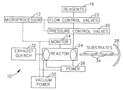
FIG. 10 schematically illustrates a plasma enhanced chemical vapor deposition
(PECVD)
apparatus 10 according to a preferred embodiment of the invention, with
physical dimensions
tailored to accommodate a pair of ophthalmic (spectacle) lenses, which may be
glass or plastic
(e.g., polycarbonate, bis-phenol A resins such as CR-39TM, available from PPG
Industries, etc.).
The PECVD apparatus includes a microprocessor 12, optical monitor 14, reagent
source 16, inlet
manifold 18, pressure control valve 20, flow control valve 22, plasma reactor
24, power supply
26, substrate holder 28, vacuum pump 30, and exhaust filter 32. Plastic or
glass ophthalmic
substrates 34,35 are mounted or placed on the substrate holder 28 and inserted
into the plasma
reactor chamber, which preferably has a volume of less than about twice that
of the substrates)
to be coated.
PECVD involves placing the substrate in a reactor chamber, passing at least
one precursor
material capable of forming the desired layer through the chamber in a laminar
flow relative to
the coating surface and at a suitable pressure, and then generating an
electric field to form a
plasma with the precursor(s). The coupling of energy into the gas occurs via
electric fields that
can be static (d.c. coupled}, or dynamic (a.c. coupled). A.C. coupling can be
either capacitive,
inductive, or both. The precursors) breaks down and reacts in the plasma and
on the coating
-11-
SUBSTITUTE SHEET (RULE 26~
CA 02279425 1999-07-26
WO 98133077 PCTIUS97/23231
I
siuface to form the desired layer. Depending on the composition of the
precursor(s), the electric
field strength, and other parameters, the film can have extended arrays of
regularly repeating
molecular constituents, amorphous regions, or mixtures of ordered and
unordered polymeric
regions.
Most of the precursor compounds listed in Table I are liquids at room
temperature and
pressure. In a preferred embodiment, the liquid precursor is degassed by
cooling it and then
subjecting it to a vacuum. Depending on its boiling point, the liquid is then
heated to ambient
temperature or higher in order to provide sufficient positive vapor pressure
to flow through a
channeling system. Alternatively, a carrier gas, such as helium, can be blown
through the liquid
to obtain a dilute vapor mixture of desired composition.
Gaseous precursors that form the AR coatings of the present invention can be
supplied
from an external source through a series of inlet pipes and into the reactor
chamber. The
technical particularities of channeling the various gases into the reactor
chamber are well-known
in the art.
The flow of carrier and reactant gases into the reactor can be controlled by
flow control
valves, which are well-known in the art and serve both to measure the flow of
gases and to
control such flow. Furthermore, the carrier gas, when used, can be premixed
with the gaseous
reactants or fed into the central feed line by a separate inlet.
As shown in FIG. 10, the pressure and flow of the precursor gas into the
plasma reactor
24 are electronically controlled by flow control valves 22. The chamber
temperature is
preferably at or near ambient temperature.
The apparatus I O includes a feedback system to allow precise control over the
deposition
of an AR coating on the substrates. The AR coating may consist of a single
layer or multiple
layers, each layer having a predetermined thickness. It is important that the
thickness of each
Iayer precisely corresponds to the predetermined design thickness to maximize
the anti-reflection
properties of the coating. The feedback system measures the thickness of each
layer as it is being
deposited and controls the deposition rate accordingly in order to precisely
control the thickness
ofthe deposited layer. The feedback system includes microprocessor I2, optical
monitor 14, and
one or more of the pressure control valve 20, flow control valve 22, and
plasma reactor 24,
including a plasma generator and a reactor chamber, and power supply 26.
Preferably, the
microprocessor is linked to all of the control values and the power supply.
The primary control
elements governed by the microprocessor 12 in response to a feedback signal
from the optical
monitor 14 are the gas flow rates through the flow control valve 22 and the
plasma excitation by
the power supply 26 for the plasma reactor 24. In some embodiments, it is
advantageous to
-12-
SUBSTITUTE SHEET (RULE 28)
CA 02279425 1999-07-26
PGT/US97IZ3231
1
regulate the chamber pressure with the pressure control valve 24 when
switching between the
steps of cleaning or etching the substrates) and depositing multiple layers of
coating materials.
The following are some examples of reflectance profiles calculated from
equations ( 1 ) -
(6) for different AR coatings. It is intended that these examples be
considered as illustrative of
the invention, rather than limiting what is otherwise disclosed and claimed
herein.
FIGS. 1 and 2 illustrate the reflectance of the s- and p-polarized components
of an
unpolarized light source from a typical two-layer AR coating on a plastic
ophthalmic substrate.
The calculation is shown for a 135 nm Iayer of fluoropolymer (CFx) over a 200
nm layer of
Si02 on a polycarbonate substrate.
FIG. 7 shows s-polarized reflectance from thin fluoropolymer films at SOOnm
optical
wavelength, calculated at six different angles of incidence ranging from 0 to
50 degrees.
FIG. 8 shows p-polarized reflectance from thin fluoropolymer films at 500 nm
optical
wavelength calculated at six different angles of incidence from 0 to 50
degrees.
The variation of p-polarized reflected light with coating thickness and angle
of incidence
is quite different from that of s-polarized light, as seen by comparing FIGS.
7 and 8. Consider
a desired film optical thickness of 125 nm measured with a green probe light
(500 nm) at an
angle of 50° as an example of this diagnostic. The s-polarized
reflectance drops from 9.6% at
90 nm optical thickness to 6% as the target thickness changes from 80 to 125
nm, as shown in
FIG. 7. Over the same range of film thicknesses, the p-polarized reflectance
drops from 0.5% to
0.4% (FIG. 8), a much smaller and more difficult change to measure accurately.
All other factors
being equal, the s-polarized signal would be selected for feedback control of
the deposition
process at a 50 ° angle of incidence of the light probe.
In other words, in one aspect of the invention, a target optical thickness is
identified for
one or more layers. and equations ( 1 ) - (6) are then solved to find the
variation of polarized
reflectances wiThth wavelength, angle of incidence, and layer thickness. One
or more angles
and one or more wavelengths are chosen to probe (monitor) the layer during
deposition. When
the reflected light intensity reaches the value calculated for the target
thickness at the chosen
waveIength(s) and angle(s), the deposition process is terminated, by e.g., the
microprocessor 12.
This approach is easily generalized to more than one layer.
In some embodiments, it is advantageous to form a multilayer, rather than a
single layer,
coating. Multilayer coatings can provide a broader spectral region with low
reflectance than can
be achieved with a single-layer coating. Other material considerations include
adhesion, scratch
resistance, chemical resistance (such as stain resistance), wear resistance,
and other desired
properties. FIG. 11 provides computed average reflectance data for one
nonlimiting example of
a two-layer coating on a polycarbonate substrate. The first layer is Ti0 with
a 180nm optical
-13-
SUBSTITUTE SHEET (RULE 26)
CA 02279425 1999-07-26
WO 98/33077 PCTIUS97123231
thickness (81.8nm physical thickness), formed by chemical vapor deposition of
Ti(i-Pr0)4. This
is followed by a layer of fluorocarbon {CFX) film ( 125nm optical thickness),
made using c-C4F8
as a precursor. Note that the region of low reflectance is broadened compared
to that found far
a simple CFX coating in FIG. 6.
As with single layer AR coatings or films, the polarized reflectance at
various angles and
wavelengths can be used to control the deposition process in the preparation
of a multilayer AR
film. For example, FIG. 12 shows the s-polarized reflectance at angles from 0-
50° for a finished
two-layer coating. A family of curves similar to those shown in FIGS. 7 and 8
for the single
fluoropolymer coating can be used to compute polarized reflectance, with
selected values of
polarized reflectance corresponding to a desired thickness triggering the
switch from the Ti0
precursor to the CFX precursor.
Unpolarized probe light may also be resolved using a polarizing beamsplitter
between the
polarization filter 54 and two matched detectors, which replace the single
detector 56 (FIG. 9).
The ratio of the detector outputs is equal to the ratio of the square of the
corresponding Fresnel
reflection coefficients, calculable from equations (1) - (6) above. This ratio
yields a response
surface characterized by the ratio of FIGS. 1 and 2 for a single thickness
film and a family of
such surfaces for a growing film or multilayer.
In some embodiments, it is advantageous to select more than one incident probe
light
wavelength and/or polarization, particularly if more than one precursor is
used, or if one
wavelength is optimal for the cleaning step and a different wavelength is
preferred for
deposition.
The composition of the substrate enters into equation (2) through its optical
admittance,
y°. As a practical matter, differences in the thickness of the
substrate do not enter the equations,
since the thickness of ophthalmic substrates is much greater than the optical
wavelengths of
incident light. The shape of the substrate does not enter the equations as
long as the ratio of the
substrate's radius of curvature through the radius of the spot of light where
the probe contacts
the lens is much greater than one, a condition that is always satisfied for a
sufficiently small
probe spot on the ophthalmic substrates.
According to one embodiment, prior to film deposition, the substrate is
cleaned by
exposing it to a plasma of inert gas ions, reactive radicals, or by other
means known in the art.
The method of generating and applying the electric field to create the plasma
is not critical to this
process. For example, the field may be generated by direct, inductive, or
capacitive coupling
systems. Non-limiting examples of such systems are found in Thin-Film
Deposition, Principle
and Practice by Don Smith, (New York: McGraw HiII) 1995.
-14-
SUBSTITUTE SHEET (RULE 25)
CA 02279425 1999-07-26
WO 98r33077 PCTIUS97/23231
1
The steps) used to clean a substrate vary with substrate composition, the
degree and type
of contamination, and the range of plasma conditions resulting from flow and
electrical
constraints of the particular plasma chamber used. It is common, for example,
to etch away
organic material with an oxygen plasma for a few minutes prior to thin-film
deposition. Etching
of organic contaminants and surface oxide can also be accomplished by
discharged halogenated
gases such as HBr.
In one embodiment, the cleaning step is initiated by activating the vacuum
pump 30 and
I O admitting Ar gas to the tube at pressures of I-20 millibar. A plasma is
ignited by applying 50
kHz power to annular electrodes mounted inside (for direct coupling) or
outside (for capacitive
or inductive coupling) of the plasma reactor 24. Electrons, Ar+ ions, excited
species, and light
impinge upon both sides of the substrate, removing adsorbed impurities and
activating the
surface for adhesion of the AR coating.
This surface preparation may modify the refractive index of the surface
layers. The
modification of the refractive index can also be used to optically monitor the
cleaning step. A
change in the refractive index of the surface layer causes a change in the
Fresnel reflection from
that surface, a change that can be measured with the optical monitor 14. The
cleaning step can
thereby be controlled using the feedback system of the present invention, as
described above, by
continuing the cleaning step until a desired refractive index corresponding to
a sufficiently
cleaned substrate is detected.
According to another embodiment, the cleaning process is monitored by
observing
fluorescence from impurities as they are purged from the plasma reactor 24.
For example,
excited OH is produced from dissociative excitation of water vapor by electron
impact, which
produces observable fluorescent emissions. As the water vapor concentration in
the plasma
reactor 24 decreases during plasma cleaning, the intensity of these
fluorescent emissions decays.
The reactor chamber is evacuated prior to entry of the gaseous reactants.
Chamber
pressures suitable for the process of the present invention are generally less
than one twentieth
of one atmosphere and typically lie within the range of about 50 mTorr to
about 10 Ton.
As the precursors) enter the reaction chamber after the coating surface is
cleaned and
treated as described above, an electric field is generated under preselected
frequency and power
conditions to ionize the gas mix, thereby forming a plasma. When a discharge
is produced at a
low pressure in the film-forming gaseous precursor(s), the precursor{s) become
ionized, forming
a plasma. A portion of the material is in the form of ions, electrons, and
neutral free radicals
generated in the plasma prior to formation of the film over or upon the
substrate. Methods of
generating an electric field between electrodes are well-known in the art and
described, for
example in Thin Film Deposition.' Principal and Practice (ibid.)
-I 5-
SUBSTITUTE SHEET (RULE 26~
CA 02279425 1999-07-26
WO 98133077 PCTIUS97/23231
1
A preferred deposition rate is between about 0.1 and 10 nanometers per second;
however,
rates up to about 65 nm/sec are possible. The deposition rate is constrained
only by the rate at
which a homogenous plasma can be produced in order to form a uniform deposited
layer.
Preferably, the AR coating is continuously deposited with no interruption
between layers.
This is accomplished by reducing the flow rate of a first precursor while
simultaneously
initiating an increase in the flow of the second precursor such that both
materials are being
deposited simultaneously. In this manner, more gradual changes in the
refi~active index profile
may be created. Alternatively, there may be cases where an intermediate
cleaning or activation
step is desirable, e.g. to relax internal stresses or improve adhesion at the
interface between
layers.
Preferably, the multilayer AR coating is "capped" with an optically thin
(e.g., ndr < 20nm)
layer of hydrophobic material. For example, a hydrophobic, polymeric
fluorocarbon film can be
made from a precursor such as a perfluorinated organic compound, e.g.
perfluorocyclobutane(c
C4F~, trifluoromethane (HCF3), tetrafluoroethylene (CZF4) or hexafluoropropene
(C3F6). The
presence of such a layer makes it easier to clean the coated substrate, and
inhibits formation of
water or grease spots.
According to another embodiment of the invention there is a smooth transition
between
the cleaning step and the deposition step. Near the end of the cleaning cycle,
deposition
precursor material is bled into the chamber, and the cleaning reagent, e.g.
oxygen, is gradually
restricted in a balanced way so that the surface is continually bombarded by
energetic particles
during formation of the first layer of film. This is important, as an impurity
present at a
concentration of even 10~' Torr will form a monolayer in less than one second.
Switching
smoothly from cleaning to deposition in this manner also improves adhesion of
the film.
PECVD by reactive ions is appropriate for coating substrates with regular, as
well as
irregular, surfaces, including the ledges found on bifocal ophthalmic lenses.
During deposition,
the direction of the ionic flux that produces the thin-film coating is
determined by the
electrostatic sheath and the ratio of the ion thermal temperature (in eV) to
the sheath potential.
The sheath is oriented normal to the tangent plane at the substrate surface
and is not modified
when the spatial scale of the structure is smaller than about 10 Debye
lengths. A Debye length
is a plasma parameter that describes the distance over which an electric field
can be maintained
in the electrically conducting plasma medium. If the number of electrons per
cubic centimeter
is Ne and the electron temperature in eV is Te~ then the Debye length, 1, in
centimeters is
-16-
SUBSTITUTE SHEET {RULE 26)
CA 02279425 1999-07-26
wo 9a~m~ rcr~rs9~n3m
I =525 (TeN~')~' (8)
Under a typical set of plasma conditions, with an electron density of 109 cm 3
and an electron
temperature of 2 electron volts (eV), this Debye length is 0.02 cm, so
features with a radius of
curvature less than about l Ot= 2 mm will not affect the direction of the
sheath electric field. The
angular divergence of the ion flux is given by the inverse tangent of the
square root of the ratio
of the ion thermal energy to the sheath potential:
a =~ 1(TfV~~ )~
This angular divergence is 9° for a typical ion temperature of
600°K and a sheath potential of
2 eV. This angular averaging produces more uniform coverage over topography
than would be
the case for a monoenergetic ion beam with no transverse energy.
Confomial coverage over steps of practical interest to ophthalmic substrates,
for example,
ledges for bifocal lenses, can be obtained by altering the plasma conditions
by, for example,
raising Te or decreasing Ne, to extend the spatial scales for conformal
coating.
It will be appreciated that, in addition to the methods and apparatus
described above, the
invention also provides unique articles of manufacture, characterized by low
reflectance.
Generally, the articles are transparent, for example, ophthalmic lenses,
windows, windshields,
television screens and computer monitors, etc. Transparent articles and
substrates have no
absorption of light over the region of the spectrum sensed by the human visual
system, that is
between about 350 and about 750 run. In some embodiments, however, the article
may be
translucent. Translucent articles and substrates transmit light at some
visible wavelengths but
absorb some or all of the Light at one or more visible wavelengths.
Nonlimiting examples of
translucent, articles include tinted and shaded sunglasses, stained-glass
windows, and tinted
windshields.
In one embodiment, a transparent or translucent low-reflection article
comprises an optical
substrate and one or more layers of AR material. Preferably, at least one of
the layers is a thin
fluoropolymer film. FIG. 13 is a schematic illustration of the cmss-section of
one such article,
a spectacle lens 100. The lens consists of an optical preform I02 having
opposed first and
second surfaces 104, 106 and a layer of AR material 108 coated (more
proecisely, deposited) on
at least a portion of the first surface 104 of the ophthalmic lens. In other
embodiments (not
shown), the AR material is deposited on the bottom surface of the lens, both
the top and the
bottom surfaces of the lens, and/or the edge of the lens.
FIG. 14 is a schematic illustration of the cross section of another low
reflection article,
an ophthalmic lens 100. The Lens consists of an optical preform 102 coated
with two different
-17-
SUBSTITUTE SHEET (RULE 26)
-16-
SUBSTITUTE SHEET
CA 02279425 1999-07-26
WO ~~ PCT/US97/23231
1
layers 110 and 112 of AR material. Both layers are considered to be deposited
or "coated" on
the optical substrate, though, as shown, only one such layer 110 is adjacent
to the substrate, the
ether layer 112 being adjacent to the first layer of AR material. It will be
readily appreciated that
low reflection articles having more than two layers of material deposited on
an underlying
optical substrate are also within the scope of the present invention.
The invention has been described in preferred and exemplary embodiments, but
is not
limited thereto. A variety of modifications, modes of operations and
embodiments, all within the
IO ability and skill of those skilled in the art, can be made without
departing from the present
invention. For example, the AR coatings and methods of designing and applying
them can be
used on a variety of optical substrates in addition to ophthalmic lenses. Even
large articles, like
automobile windshields, can be given an AR coating if a suitably large reactor
is built.
All references herein are incorporated by reference as if set forth herein in
their entirety.
1 S In both the text and the claims, use of the word "about" in relation to a
range of numbers is
intended to modify both the high and low values stated.
25
35
-18-
SUBSTITUTE SHEET (RULE 26)