Note: Descriptions are shown in the official language in which they were submitted.
CA 02279505 1999-08-03
WO 98/33665 PCT/US98/01093
FORMATION OF SUPERCONDUCTING DEVICES USING
A SELECTIVE ETCHING TECHNIQUE
TECHNICAL FIELD
This application relates to a method for selectively etching portions of
superconducting materials to produce a superconducting device with a desired
configuration. The inventive method uses ion implantation in conjunction with
chemical etching to produce microscopic superconducting devices.
BACKGROUND OF THE INVENTION
Recent progress in high temperature superconducting (HTS)
electronics has demonstrated that HTS materials can provide faster, quieter
and more
precise electronics for the 21 st century. A HTS device could switch much
faster and
require much less power than a silicon transistor, have several orders of
magnitude
lower microwave loss than that of a metal at satellite operating frequencies (
10-60
GHz) and even detect human brain signals with the highest sensitivity. The HTS
devices currently under development include Josephson junctions,
superconducting
quantum interference devices (SQUIDS), radio frequency (RF) coils, bolometers,
and
microwave components. The Josephson junctions are the building blocks of
superconducting digital circuits for ultra-fast computers and communication
systems.
The SQUID has a variety of applications, including magnetic, non-invasive
diagnosis
for the human heart and brain, non-destructive evaluation for many structural
materials, and geophysical exploration. The RF coils made of HTS have shown a
great improvement in signal-to-noise ratio or image resolution in MRI
(magnetic
resonance imaging) systems. A HTS bolometer built on silicon membrane is very
sensitive in order to detect radiation and small changes in temperature.
Prototypes of
CA 02279505 1999-08-03
WO 98/33665 PCT/US98/01093
2
HTS microwave devices have a superior performance in both space and cellular
communications.
The full realization of these HTS devices depends on the development
of reliable processing technology. Due to the fact that HTS materials are
oxides (e.g.,
YBaCUO and TIBaCaCuO), they are very sensitive to the environment such as
moisture, chemicals, and water. The surface reaction usually decomposes the
surface
layer of the materials and degrades the performance of the devices. As a
result, the
yield of the HTS devices by conventional etching methods is very poor, e.g.,
only 15-
20%.
Chemical etching is one possible way to configure a desired design in a
superconducting thin film. However, the strong thermodynamic driving force
necessary in the etching process due to the formation of hydroxides and
carbonates
degrade the HTS materials significantly. Previous etching methods that had
been
developed have a typical duration of about 3-16 minutes in contact with the
etching
agent assuming a 3000 A thick film. This long etching time causes an increased
surface resistance of the films and loss of its superconducting properties due
to the
increased chemical reaction. A rapid etching process is therefore required to
reduce
the possibility of degradation of the superconductivity at the surface of the
films. The
etching process must remove the unwanted portions of the film while retaining
the
selected portions in a short period of time.
Ion implantation has been widely used for doping semiconductor
devices. Recently, ion implantation has also been applied for inhibiting
superconductivity in HTS films and for patterning HTS planar devices (See Ma
et al,
"A Planar Method for Patterning HTS Films and Multilayers" Aat~~ 1 Phys.
Lett., Vol
65, p. 240, 1994]. In this process, a portion of a HTS film in inhibited with
reactive
ion implantation and the portion converts into non-superconducting material.
The
uninhibited portion remains superconducting as the device region, surrounded
by the
inhibited region. Thus, the applications for this type of device is limited to
a fully
layered structure.
CA 02279505 1999-08-03
WO 98/336b5 PCT/US98/01093
3
SUMMARY OF THE INVENTION
The invention provides a method for forming a designed thin film
superconducting device using a selective etching technique. The technique
allows for
the selective patterning of superconducting thin films either as a single
layer or as a
multi-layered device. The inventive method forms a superconducting layer on
top of
a substrate material. A mask is then applied to cover selected portions of the
superconducting layer and ions are implanted into the layer. Next, a chemical
etching
technique such as an acid bath is applied to remove the portions of the
superconducting layer which were not masked and ion implanted. The resulting
device can be configured to be used, e.g., as HTS nanostructures such as carry
confined devices, 3osephson junctions, SQUIDs, RF coils, bolometers, microwave
waveguides and filters. The process enables microscopic superconducting
devices to
be produced.
The selective chemical etching processes can be modified by altering
the chemical etching solvent and by altering the type of ion implantation
(both ion
type and energy level). The ion implanted superconducting thin films will be
removed during the chemical etching process at a much higher rate than the non-
implanted regions. A thicker superconducting film or a superconducting bulk
wafer
can also be used in place of the substrate if required.
BRIEF DESCRIPTION OF THE DRAWINGS
Further objects, features and advantages of the invention will become
apparent from the following detailed description taken in conjunction with the
accompanying drawings showing the preferred embodiments of the invention,
in which:
Figure 1 is a flow chart of the steps for forming a superconducting
device using a selective etching technique;
CA 02279505 1999-08-03
WO 98/33665 PCT/US98/01093
4
Figure 2 shows a single layer superconducting device being
constructed in accordance with the invention;
Figure 3 shows a mufti-layered superconducting device being
constructed in accordance with the invention;
Figure 4A shows a superconducting device constructed in accordance
with the invention with a protection layer;
Figure 4B shows an alternative superconducting device with a
protection layer;
Figure 4C shows a mufti-layered superconducting device with a
protection layer;
Figure 5 shows a table comparing etching rates between pure and ion
implanted HTS structures;
Figure 6 shows a graph of the data from Fig. 5;
Figure 7A shows a bolometer made in accordance with the invention
1 S prior to chemical etching;
Figure 7B shows a bolometer made in accordance with the invention
after chemical etching; and
Figure 7C shows a top view of the bolometer made in accordance with
the invention.
DESCRIPTION OF A PREFERRED EMBODIMENT
The present invention forms superconducting devices using a selective
etching technique. Superconducting thin films are formed on substrates and can
be
patterned to a desired configuration. The substrate could be an IC chip wafer
or made
from conventional oxide materials, such as SrTi03, LaAl03, A1203, or MgO. The
use
of an ion implantation device set to the proper energy level in conjunction
with the
use of a mask or masks covering selected portions of the superconducting layer
allows
for the removal of the ion implanted portions of the layer during the chemical
etching
process at a much higher rate than the region not implanted. If the
concentration level
CA 02279505 1999-08-03
WO 98/33665 PCT/US98/01093
of the chemical etching agent (typically an acid) is low enough, the un-
implanted
regions will not be dissolved at all. However, all of the ion implanted
regions will be
dissolved. Therefore, only the selected regions of the superconducting thin
film
covered by the masks will remain. The etching process is greatly speeded up
due to
5 the ion implantation and this reduces any degradation in the remaining
superconducting portions.
The preciseness and microscopic size of the ion beam from the ion
implantation device allows for fine patterns to be produced in the
superconductor
film. The inventive process can produce superconducting devices even on the
nanometer order of size. Some examples of the superconducting devices which
can
be produced are a Josephine junction, bolometer, RF coil, and a waveguide.
These
tiny devices and other designs can be used in an ultra-miniature chip, sensor
or
electronic component design. One example of a use for such a small device is
as the
tip for a scanning tunnelling microscope which detects obj ects as small as
atoms.
Figure 1 shows the steps in the method for forming superconducting
devices using a selective etching technique. Examples of the application of
these
steps will be shown in subsequent figures. The method of Figure 1 allows for
very
small superconducting micro-structures, even including nano-structures, to be
created
without destroying or distorting the superconducting properties of the created
structure.
Step 101 disposes a superconducting thin film on a substrate upon
which the structure is to be created. Examples of high temperature
superconducting
materials which can be used in TBCCO or YBCO. The film's thickness will vary
by
application. In this described embodiment, the thickness is between 300A to 1
pm.
The substrate material also varies depending upon the intended use of the
structure.
The results of this method is to selectively etch away portions of the HTS
film and
leave only the intended structure in a short period of time without damaging
the
desired superconducting structure.
Step 103 aligns a mask above the selected portions of the HTS films
which are to remain. An example of a mask is a photoresist mask formed by
normal
CA 02279505 1999-08-03
WO 98133665 PCT/LTS98/01093
6
photolithology which will inhibit ions from implanting in the underlying
superconducting material during the following implantation step.
Step 105 then implants ions into the structure with an ion implanter
device or other conventional method. An example of an ion implanter device
which
can be used is an Eaton's 3206. The ions are implanted in the direction such
that the
mask is first encountered before the HTS film. Different energies of ion
implantation
can be used. The ions can be selected from single ions such as Si, Al, B, Ni,
Fe, Ca,
Ti, Mn, Mg, Co, P and Sr or ion molecules (Si02 and Si3F4). For the materials
described herein, the energy level should be between 10 keV to 500 KeV and the
does
of 1 x 10'3 to 1 x 10"/cm2. The ion implantation will change the properties of
the
portions of the HTS film which are not covered by the mask.
Step 107 then chemically etches the entire structure. The chemical
etching is preferably performed by applying an etching agent such as
phosphoric acid
to the structure. The application of the etching agent can be achieved by
submersing
the structure in an acid bath, by selectively applying the acid to the desired
region or
by any other conventional method. The acid will remove the portions of the HTS
film
which have been ion implanted much faster than the portions which have not
been
implanted (described in more detail below). Therefore, after a specified
amount of
time in contact with the dissolving agent, the structure can be removed from
the
etching agent leaving only that portion of the structure which was masked by
the ion
implantation. This allows for the creation of HTS devices in the desired
pattern for a
selected application. Phosphoric acid can have a concentration of 1.5X10⁻³ M
to only
etch out the implanted regions. After the acid bath, the etched
superconducting device
may be annealed with a furnace or a rapid thermal annealer at 450C for a short
period
of time (30 seconds to 30 minutes) to strengthen the resulting device.
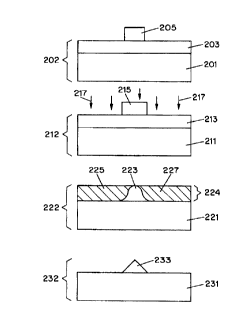
Figure 2 shows an example of the method of Fig. 1 being applied to
form a selected HTS device. The structure (device) is shown in its four phases
of
manufacture.
Structure 202 shows a substrate 201 upon which a HTS thin film 203
has been deposited. A mask 205 is also aligned over the HTS thin film to
ensure that
CA 02279505 1999-08-03
WO 98/33665 PCT/iJS98/01093
7
the portion under the mask will not be ion implanted during the implantation
stage.
The mask 205 in this example is an electron-beam lithographic mask with a
width of
0.1 pm. The mask could be configured in any manner and multiple masks could be
used on the same HTS film if needed.
Structure 212 shows the structure during the ion implantation step.
The HTS film 213 is ion bombarded with ion beams 217. The mask 215 blocks the
ion beam from entering the HTS thin film directly below it. The ion beams 217
may
enter the substrate 2I 1 depending on the HTS film's thickness but have no
consequential effect on the substrate.
Structure 222 shows the structure after the ion implantation operation
is completed. The mask has now been removed leaving only the substrate 221 and
the
HTS film 224. Portions 225, 227 of the HTS film 224 which were not covered by
the
mask have been ion implanted. The portion 223 of the HTS film 224 which was
covered by the mask is not ion implanted. The portion 223 will typically have
a bell
shape due to transverse straggling of the ion beam with respect to the masked
portions. For this example, the tails of the bell shape will typically be
about 100 A
wide for a 0.1 pm mask.
Structure 232 shows the structure after its has been selectively
chemically etched. The structure has been submitted to a chemical etching
solution
and the portions of the HTS film with ion implantation have been removed. If
the
structure is left in the etching solution for a few more seconds after the ion
implanted
portions are removed, the non-ion implanted portions will also begin to be
etched
away at a slower rate if the etching solution concentration is high enough.
Thus the
bell shaped region 223 will be modified to now have a roughly triangular shape
233
with a sharp tip having a dimension less than 100 A or a few atomic units in
distance.
The only remaining portions of the structure will be the substrate 231 and the
HTS
device 233. The structure 232 can now be used for individual applications or
combined with other structures depending upon the design specifications.
CA 02279505 1999-08-03
WO 98/33665 PCT/US98/01093
8
Figure 3 shows an example of the method of Figure 1 being used to
form a mufti-layered structure which allows for a greater range of shapes
which can
be used as a HTS device.
Structure 301 includes a substrate 303 upon which a HTS thin film 305
has been deposited. A mask 307 covers a portion of the HTS film which is
desired to
be retained in a similar manner as shown in Fig. 2. Ion beams 309 are applied
to the
structure 301 to implant the unprotected portions.
Structure 311 shows the results of the ion implantation. The substrate
313 now supports HTS film portion 318 which has not been ion implanted and HTS
film portions 316, 317 which have been ion implanted. The mask has also been
removed.
Structure 321 shows a new HTS thin film 327 being deposited upon
the substrate 323 and HTS layer 325. This step is performed prior to the
selective
etching process. A new mask 329 is applied to cover the portion of the second
layer
327 which is to remain in the resulting device. The second mask 329 must cover
the
entirety of the portion of the first HTS film which is to remain in the device
so that the
second ion implantation step will not implant the first portion. Ion beams 331
are
then applied to the structure 321.
Structure 341 shows the results of the second ion implantation before
any chemical etching is performed. The first HTS thin film layer 345 is
deposited on
substrate 343 and the second HTS thin film layer 347 is deposited on the first
thin
film layer. Portion 355 in the first thin film layer and portion 349 in the
second thin
film layer have not been ion implanted because of the placement of the
respective
masks. Portion 357, 359 of the first HTS thin film layer and portions 351, 353
of the
second HTS thin film layer have been ion implanted in the process previously
described.
Structure 361 shows the remaining structure after structure 341 has
. been chemically etched. The portions of the HTS thin films which has been
ion
implanted are etched at a much faster rate so that they are removed to leave
the
portions which were not ion implanted. The non-ion implanted (pure) regions
will not
CA 02279505 1999-08-03
WO 98/33665 PCT/US98J01093
9
be etched at all or, depending on the acid concentration, will be etched at a
relatively
slow rate so that there will be no significant deterioration in the resulting
device. This
layering method can be repeated as need in order to form a desired device
configuration.
One such device configuration is a multiple RF coil device for
receiving multiple resonance frequencies. The RF coils are configured on each
superconducting layer with the use of masks. In Fig. 3, layer 365 has one or
more RF
coils and layer 367 has one or more RF coils. This allows the device 361 to
detect
and receive multiple frequencies within the single device.
Figures 4A, 4B and 4C show superconducting devices which can be
created with the techniques of the present invention and the addition of a cap
or
protecting layer. The protection layer is deposited on top of the
superconducting layer
when it is formed so that the superconducting layer will not react with other
chemical
constituents which it comes in contact with after leaving a "clean"
environment, such
1 S as a clean room.
Many HTS materials are oxide materials which make them very
reactive. Examples of materials which can be used as protecting layers are
SrTi03,
Ce02, Au, Ag, Mg0 or LaAl03. A preferred thickness for their protecting layer
is 50-
1000~ on a thin film which is 0.1 - 1 pm thick.
Figure 4A shows a structure 400 with a single layer HTS thin film 403
deposited on a substrate 401 covered by a protection layer 405. The protection
layer
405 is thin enough so that it does not materially diminish the ion beam in the
ion
implantation process. Two masks 407, 409 are placed on the edges of the HTS
thin
film to protect the underlying portions 41 I, 413 from the ion beam. The
center
portion 415 which is not protected by a mask is ion implanted by the ion
beams. A
small opening 408 is made or formed in protection layer 405 so that the
chemical
etching solution can work on the center of the HTS film layer 403 during the
etching
process.
CA 02279505 1999-08-03
WO 98/33665 PCT/US98/01093
After the structure 400 is chemically etched, superconducting device
421 remains. The center portion 423 of the device has been removed. The
resulting
structure can be used as a wave guide device, for example.
Figure 4B shows a structure that is constructed in a similar manner to
5 that described in Fig. 4A except the bottom substrate layer is replaced with
a thicker
superconducting material, superconducting film or a superconductor bulk wafer.
Structure 445 contains a HTS base 447 and a protection layer 449 deposited on
it.
Two masks 451 and 453 are placed over the protection layer so that the
portions of the
HTS material under the masks will not be ion implanted. Ion beams 455 are then
10 directed at structure 445 so that the center of the HTS material will be
implanted with
ions.
When an ion beam is directed at structure 445, the ion beam loses
potency after penetrating a HTS material for a certain distance. In this
example, the
superconducting material will remain below the implanted range, 0.1 to 1 pm in
depth
from the film surface. The ion beam when applied to the thicker HTS film will
only
penetrate partially into the material. Thus in this example, the portions not
covered by
masks will only be penetrated in their top portions. Therefore, after
chemically
etching the structure, only the center portion of the HTS portion will be
removed.
The protective cap will be affixed to the top of the structure as in Fig. 4A.
This new
structure after chemical etching will appear as structure 457 which can act as
a wave
guide like structure 421 in Fig. 4A but will have different characteristics
because of
the additional superconducting materials in place of the substrate.
Figure 4C shows an example of multi-layering HTS films with
protection layers which allows for further patterns and designs of
superconducting
devices to be created.
Structure 461 shows the structure in Figure 4A after ion implantation
but before the chemical etching process is performed. HTS thin film 465 has
been
deposited upon substrate 463 and protection layer 467 has been deposited upon
HTS
thin film layer 465. Center portion 473 has been ion implanted but portions
469 and
CA 02279505 1999-08-03
WO 98/33665 PCT/LTS98/01093
11
471 have not been implanted because of the placement of the masks during the
ion
implantation process.
Structure 473 now shows an additional HTS thin film 475 being
deposited on top of the protection layer 467. A second protection layer 476 is
deposited on top of the additional HTS film 475. The HTS thin film can then be
masked such that only selected portions of the second layer will remain after
the
chemical etching process. A second ion implantation step will then ion implant
the
regions of the second layer which are not covered by masks. The mask
configuration
must be placed such that the first HTS thin film layer will not be affected by
the
second ion implantation. This can be accomplished by making the first
protection
layer thicker or by inserting a relative thick buffer layer between the first
protection
layer and the second HTS layer 475. The buffer layer may use the same material
as
the protection layer. Masks 476 and 477 are shown in this example.
Structure 480 shows structure 473 after it has been masked, ion
implanted and chemically etched. The chemical etching process has removed the
ion
implanted HTS thin film portions. The resulting structure can by used as
waveguides
or as RF coils in microwave devices. The resulting structure comprises a
substrate
482 upon which selected portions 484 of a HTS film remain. A protective layer
486
is on top of the first selected portions 484 and the second selected portion
488 of the
second HTS thin film is on top of the protective layer. Finally, a second
protection
layer 490 is on top of the second selected portion 488. The layering effect
can be
continued as needed.
Figure 5 shows a table containing the etching rates of HTS materials in
different concentrations of phosphoric acid. The results confirm that the
process of
the present invention can quickly yield superconducting devices. Column 501
shows
the concentration of phosphoric acid used in the chemical etching phase of
construction. Category 503 shows the etching rate of YBCO, a superconducting
material, under different conditions. These conditions are: (1) when there in
no ion
implantation (column 505); (2) when it has been implanted with 200KeV of Al3+
(column 507); (30} when it has been implanted with 120KeV of Al3-; and (4)
when it
CA 02279505 1999-08-03
WO 98/33665 PCT/US98/01093
12
has been implanted with 100 KeV of Fe3+. The data shows that the etching rate
for the
implanted superconducting films is greater than that for the pure non-ion
implanted
HTS films. This is especially true for lower concentrations of acid where the
difference in rates is great. By selecting the proper ion to implant and the
proper
energy level for the ion, the etching rate can be selected as required for any
manufacturing process. The etching rate in an implanted material is about 2-5
times
higher than that in a pure film when using the proper ion energy and the
proper acid
concentration.
Category 513 shows the etching rates for a different type of HTS
material, TBCCO. Column 515 shows the pure non-ion implanted HTS material and
column 517 shows the ion implanted material. Again, the etching rate for the
implanted mater is drastically higher. The etching rate for YBCO is about 4-10
times
higher than that of TBCCO for etching solution above 1x10-' M. The improved
etching rate from the present invention can help prevent degradation at the
surface of
HTS materials and lead to a better way of patterning.
Using phosphoric acid with concentration higher than Sx10~2 M, the
etching rate in an ion implanted film is much faster than that in a pure film.
Below
the threshold concentration of 1.5x10-' M, the acid has no etching affect on a
pure
film while it still etches an implanted film. This allows for more precise
construction
of semiconductor miniature devices because the non-implanted regions will
remain
fully in tact. The etching rate of the Al3+ implanted film at an energy 200
KeV is
faster than that of the A13+ implanted film at an energy 120 KeV.
Additionally, the
etching rate of Al3+ implanted film is faster than Fe3' implanted film. A
selective
etching process can be developed for HTS film using a proper etchant in
combination
with ion implantation.
It is known that high quality single-phase YBCO and TBCCO
materials have yielded unstable binding and defects on the surface and inside
of the
superconducting materials after ion implantation. Since the lattice is intact
dilation,
the binding energy is decreased, but only a small change occurs, which does
not cause
lattice parameters to change very much. It has been reported that epitaxial
YBCO
CA 02279505 1999-08-03
WO 98/33665 PCT/US98/01093
13
films can be grown on top of ion inhibited HTS films which is insulating
produced by
Si implantation. The etching procedure involves, first, the chemical reaction
between
phosphoric acid and alkaline earth elements, as the following reaction shows:
6H3P04+4YBazCU30,=
2YP04+Ba3(P04)Z+CU3(P04)z+YZBaCU05+7Cu0+BaCUOz+3Ba(OH)z+2H20+Oz.
The second stage is the collapse of lattices in the crystal. The more defects
and the
greater the unstable binding on the surface and in the lattices, the more
chances for
chemical reaction, and thus a greater chemical etching rate is expected.
Figure 6 shows a graph of the data points from Fig. S. Line 607 shows
the etching rate verses the etching acid concentration for pure YBCO (non-ion
implanted). Line 601 shows the etching rate verses the acid concentration for
Al ions
at 200KeV. Line 603 shows the etching rate verses the acid concentration for
A1 ions
at 120KeV. Line 605 shows the etching rate verses the acid concentration for
Fe ions
at 100KeV. The graph shows visually that the HTS material implanted with ions
is
etched at a much greater rate than the un-implanted material so that the
superconducting materials can be formed is this manner.
Figures 7A , 7B, and 7C show a bolometer device produced by the
inventive method. A bolometer can detect very small changes in temperature by
changing its resistance which can then by measured and quantified. The
bolometer
can also detect changes in different forms of radiation. A bolometer can be
more
effective if the active part of the device is thermally isolated, for example,
as a free
standing structure.
Figure 7A shows a bolometer 701 which has a substrate layer 703, a
first superconducting thin film layer 705 and a second superconducting layer
707.
Protective layers can also be inserted on top of the superconducting layers.
Portions
of the superconducting layers have been masked and ion implanted. The regions
709,
711 and 713 have been ion implanted.
Figure 7B shows the bolometer of 7A after it has been chemically
etched. Bolometer 723 now has a free standing top superconducting layer 723
which
CA 02279505 1999-08-03
WO 98/33665 PCT/US98/01093
14
is positioned over an air gap. The air gap thermally isolates the active part
of the
bolometer from the rest of the structure.
Figure 7C is a top view of bolometer 721. The top view shows the
remaining superconducting portions 723, 725 and 727 which form the bolometer
sensing circuit. The superconducting terminal portions 723, 725 are located on
the
superconducting first layer 705. Superconducting portion 727 is located on the
second superconducting layer 707 and is elevated from the first
superconducting layer
705. This mufti-layered structure allows for thermal isolation of the sensing
portion of
the bolometer.
The foregoing merely illustrates the principles of the invention. It will
thus be appreciated that those skilled in the art will be able to devise
numerous
systems, apparatus and methods which, although not explicitly shown or
described
herein, embody the principles of the invention and are thus within the spirit
and scope
of the invention as defined by its claims.