Note: Descriptions are shown in the official language in which they were submitted.
CA 02279632 1999-07-30
Method for Tuning the Wavelength of an Array
of Optoelectronic Components
The present invention relates to a method for tuning an
array of optoelectronic components that includes at least two
optoelectronic components and at least one resistance heater that
is associated with the component and includes an electrical
conductor, this being used to adjust the characteristic
wavelength of the component.
Optical transmission systems are being used to an
ever-increasing extent for transmitting data or for transmitting
television and radio channels. In general, such an optical
transmission system comprises a light-conducting wave guide, a
semi-conductor laser as the light generator, and a photodetector.
The semiconductor laser radiates light at a specific,
characteristic wavelength. This characteristic wavelength is
essentially dependent on the material that is used, although it
can be adjusted within a certain range of wavelengths, for
example by thermal action. In order to increase the quantity of
data that can be transmitted by way of a wave guide, it is
possible to use a plurality of semiconductor lasers that are
associated with a wave guide, these lasers then working at
different wavelengths. However, when this is done, it is
essential that the wavelength can be maintained very precisely,
-1-
CA 02279632 2005-03-02
28030-41
so that it is possible to differentiate unequivocally
between the data at the end of the transmission.
Because of the fact that the characteristic
wavelength of semiconductor lasers differs within a range of
tolerances, depending on producticn factors, the
semiconductor lasers must be tunes prior to being used for
transmitting data. To this end, cne uses, for example, so-
called resistance heaters that change the characteristic
wavelength of a semiconductor laser by thermal action, using
an electrical conductor that is attached to a substrate.
Generally speaking, tuning is carried out by adjusting the
voltage that is applied to the electrical conductor of the
resistance heater, a power source being associated with each
resistant heater.
However, this entails tre disadvantage that a very
costly design is required. Furthermore, it is no longer
possible to retune the circuit in a simple way.
For this reason, it is the objective of the
present invention to describe a simple method of tuning
optoelectronic components that can be carried out at any
time.
This objective of the present invention has been
achieved by a method characterizes. in that in a first step,
the wavelength of at least one con.ponent is determined, and
deviation from the desired wavelength is determined on the
basis of this value. Then, in a second step, the resistance
value of the electrical conductor of the resistance heater H
that is associated with the particular component and/or the
resistance value of a resistant circuit RM that is
incorporated ahead of the resistance heater H is changed as
-2-
CA 02279632 2005-03-02
28030-41
a function of the wavelength deviation that has been
determined. The desired change to the characteristic
wavelength is effected by purposeful alteration of the heat
output of the resistance heater H.
In accordance with this invention, there is
provided a process for the wavelength tuning of an
optoelectronic component arrangemE~nt, with at least two
optoelectronic components L1, ..., Ln, wherein the
characteristic wavelength is set for each optoelectronic
component using the principle of the thermal setting of the
characteristic wavelength by means of separately assigned
resistance heaters H1, ..., Hn, the wavelength deviation being
determined on the basis of a comp~.rison of the measured
wavelength with the characteristic wavelength, characterized
in that the thermal change of the resistance heater H1, ..., Hn
required for setting the characteristic wavelength of the
optoelectronic component is accom~~lished by selectively
changing the resistance value of the conductor of the
resistance heater H1, ..., Hn and/or by selectively changing
the resistance value of a resistor arrangement RM1, ..., RMn
connected upstream of the resistance heater H1, ..., H".
This method permits verb simple adjustment of a
plurality of optoelectronic elements in an array of
components, for example a line of semiconductor lasers. In
particular, the method can be carried out completely
automatically, which is a great aovantage if a large number
of optoelectronic components are teing used.
It is a particular advantage if the resistance
value of the electrical conductor of the resistance heater H
can be changed by alteration of the material, for example by
the precise addition or removal of material.
-3-
CA 02279632 2005-03-02
28030-41
Additional advantageous versions of the method
according to the present invention are set out in the
secondary claims. The present in~~ention will be explained
' in greater detail below, using emx>odiments that are shown in
the drawings appended hereto. These drawings show the
following:
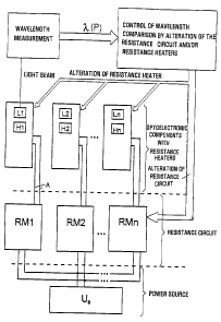
Figure 1: A block diagram of an array of
optoelectronic components;
Figure 2a: A schematic diagram showing a
resistance system;
Figure 2b: A circuit for the resistor system;
-3a-
CA 02279632 1999-07-30
Figure 2c: A diagram showing how the heat outputs of
different channels affect each other;
Figure 3: A first embodiment of a component array;
Figure 4a: Another embodiment of a component array;
Figures 4b-4d:
Three
diagrams
used
to
determine
heat
output:
Figure 5a: Another embodiment of a component array:
Figure 5b: A diagram for calculating heat output;
Figure 6: Another embodiment of a component array:
Figure 7: Another embodiment of a component array;
Figure 8: Another embodiment of a component array:
Figure 9: Another embodiment of a component array;
Figure 10: Another embodiment of a component array;
Figure 11: Another embodiment of a component array;
Figure 12a: A diagram showing a component array with a
resistance circuit that serves as a heater;
Figure 12b: A diagram that illustrates the method.
Figure
1
shows
a
component
array
1
that
comprises
a
number of
semiconductor
lasers
L1
to
Ln.
The
fundamental
con-
structi on such a line of semiconductor lasers is known, for
of
which no further description of this will be attempted
reason at
this point. In order to transmit data simultaneously in an
optical data-transmission system, the semiconductor lasers L1 to
Ln operate at different wavelengths or frequencies. Because of
certain production factors, the semiconductor lasers L1 to Ln do
not always radiate at the desired wavelength. For this reason,
they are tuned to the desired wavelength before and/or during
-4-
CA 02279632 1999-07-30
operation, this being done by changing the characteristic
wavelength; in the present case, the thermal effect is used to
tune them in this way. If a specific temperature is allowed to
act appropriately on the individual semiconductor lasers L1 to
Ln, it is possible to vary the characteristic wavelength within a
specific range. To this end, at least one resistance heater H1 to
Hn is associated with each semiconductor laser L1 to Ln. Each of
the resistance heaters H1-Hn consists of an electrical conductor
(subsequently also referred to as a current conductor): this has
l0 an appropriately high electrical resistance, generates heat when
a voltage is applied to it, and generates the desired temperature
field within the semiconductor lasers L1 to Ln. The voltage can
be supplied to the resistance heaters H1 to Hn indirectly by way
of resistance circuits RM1 to RMn (Figure 1) that are powered
from a common power supply Uo. Each of the resistance circuits
RM1-RMn is preferably built in the form of a resistor array that
consists of individual resistance elements. Changing the total
resistance, of the resistance circuit RM1, for example, changes
the heat output of the resistance heater H1. This also changes
the current flowing through the resistance heater H1. Adjustment
of the resistance circuit RM1-RMn to a specific resistance value
can be effected electrically, optically, and/or by
electromagnetic waves.
The resistance circuits RM1-RMn can be arranged, on the
one hand, on a supporting surface that bears the semiconductor
lasers L1-Ln. It is also possible to keep the resistor circuits
-5-
CA 02279632 1999-07-30
RM1-RMn separate from the semiconductor lasers L1 to Ln, for
example, in a location within the overall data transmission unit
that will subsequently be easy to access.
The voltage that is required to heat the
conductors of the resistance heaters H1 to Hn, which is supplied
by the power source Uo, is supplied through current feed lines. As
an example, these current feeds are formed from the areas A and
the bonded connections B. The areas A are formed as connections
and conductive areas that are not resistors in the true sense.
The current conductors of the resistance heaters H1-Hn consist of
a number of re-entrant conductive areas that are electrically
interconnected and which each have a total resistance RH. Each
conductor generates a heat output PH that affects the
characteristic wavelength of the semiconductor lasers L1-Ln.
In order to adjust the heat output of each resistant
heater H1-Hn to a desired value, one can change the voltage of
the voltage supply units U,,; and/or the resistance value RH of the
conductors of resistance heaters H1-Hn.
In order to adjust the heat outputs of the individual
resistance heaters H1-Hn it is advantageous to change their
resistance R, since changing the voltage affects the heat outputs
of all the resistance heaters H1 to Hn.
According to the present invention, adjustment of the
resistance RH is effected by the addition and/or removal of
material at specific locations of the conductor or uniformly
over the conductors of the resistance heaters H1-Hn. The cross
-6-
CA 02279632 1999-07-30
section of the conductor through which a current flows can be
enlarged by the addition of conductive material, and its
electrical resistance reduced thereby. In contrast to this, the
cross section of the conductor through which current flows can be
reduced by the removal of material, so that its resistance is
increased. As an example, it is possible to remove material
deliberately from specific locations by using a laser. Methods
other than laser ablation can also be used.
Apart from the addition or removal of material, which
is to say changing the cross-section of the conductor through
which current flows, it is also possible to change the material
of the conductor by mixing material into it or removing material
from it. Given the appropriate selection of the material for the
conductor, its resistance can be changed, for example, by
heating, cooling, chemical treatment, electrochemical treatment,
particle implantation, electromagnetic irradiation, and/or
particle irradiation.
In order to generate the desired temperature fields, in
addition to changing the spatial arrangement of the conductors of
the resistance heaters H1-Hn and changing the resistance of the
conductors, it is also possible to incorporate resistors in the
current feeds to the electrical conductors of the resistance
heaters H1-Hn; this can be done by using the resistor circuits
RM1-RMn.
CA 02279632 1999-07-30
As discussed heretofore, the characteristic wavelength 2~q of each
individual semiconductor laser Lq, can be adjusted individually
by way of the temperature of the appropriate semi-conductor laser
Lq and thereby by way of the heat output PH or the by the heating
current IH flowing through the resistance heater Hq associated
with the semiconductor laser Lq. The basic principle for each
channel q, with q E [l, n] to adjust the heater current
individually, can be realized by a matrix-like arrangement of the
kind shown in Figure 2 for channel q. The matrix arrangement
comprises contact fields KG,i,~ with the coordinates (i,j), i
[1,r] and j E [1,s] X, q indicating the component number
(channel), and r or s indicating the size of the matrix-like
resistance circuit in the y and x directions. The j and i
indices that are indicated show the column and row numbers. This
matrix-like arrangement of contact fields will hereinafter be
referred to as the contact matrix. The contact fields are
coupl ed through Ohmic res i stors Rq, i, ~ .g, k, l , with R9, i, ~ ~q, k,1
indicating a resistance between the contact fields Kg,i,~ and
Kg,k,l. The resistance values of the Ohmic resistors range from
2o R9, i,; _ q, k, l = 0 Ohm ( short circuit ) to R~, i, ~ ~g, k,1 ~ ~ ( no
electrically
conductive connection or insulator). The contact fields Kq,t," and
K~,~,W (t,u) # (v,w) are connected to an electrical power source Uo
that generates a potential difference U(t) of any time derivative
trend with respect to time. The electrical connections of the
power source U_, to the contact fields K~~, t, a and K~, ~,w are
hereinafter designated LQ. An electrical connection LQ consists
_g_
CA 02279632 1999-07-30
of a number f >_ 1 in the mathematical sense reentrant of
electrically conductive areas, that are interconnected
electrically. These areas contain a number g >_ 0 of electrically
conductive areas of the resistance heater Hq of a channel q and a
number h _> 0 of electrically conductive areas of the matrix-like
arrangements of contact fields.
The contact fields Kq,a,b and Kg,~,d with (a,b) ~ (c,d) are
so connected to the resistance heater Hq by an electrically
conductive connector that a difference of potential between the
points Kg,a,b and Kg,~,d causes current to flow through the resistance
heater Hq in the event that the resistance RH,g of the resistance
heater Hq is ultimately great.
The arrangement of the power source Uo, electrical
connection LQ, matrix-like arrangement of contact fields, the
Ohmic res istors Rg, i, ~ ~ q, k,1 between the contact fields Kq, i, ~ , and
Kg,k,l is so manipulated or tuned according to the present
invention that a heat output P~ is set at the electrical
resistance heater H~3; because resistance heater Hg is thermally
coupled to the semiconductor laser Lq, this causes a temperature
change ~t~ at the semiconductor laser Lg. This temperature change
induces a wavelength shift ~?~~ of the characteristic wavelength of
the channel q.
Individual adjustment of the wavelength Ag of the
channel q by changing the resistance of the conductor and/or of
the resistance circuit is effected as follows:
_g_
CA 02279632 1999-07-30
At the beginning of the process, a heat output Pq z 0 is
set up, and this results in a wavelength l~q. The objective is to
so adjust the heat output that it equals leg, S.
The heater output of the resistance heater is varied
within a range in which the desired wave length change that is
connected to this covers the range of the desired wavelength Aq,s.
This measurement results in a functional relationship 1~g(Pq).
Accordingly, the heater output Pq can be determined for a wave
length Ag,s from this relationship.
l0 The desired heat output Pg can be adjusted by changing
the resistance of the resistance circuit RMq and/or the
resistance RHg of the conductor of the resistance heater. The heat
output Pg can also be varied by adjusting the voltage at the
voltage supply Uo, although this will mean that the heat output of
the other optoelectronic components will be varied accordingly.
For example, in the case of the resistance circuit Rmq, the
maximum size of the capacity variation OPg = Pg,maX - Pq,min of a
channel q can be determined by the size of the applied voltage on
the contact fields K~,t,u and Kg,~,W, the dimensioning and
arrangement of the resistors R~, i, ~ ~ ~, k,1, and by bridging ( short
circuits) between the contact fields, as well as by measuring the
size of the heating resistor RH,g. This output variation ~pq
yields a maximum wavelength variation ~Aq,~nax~
A further possibility for adjusting the
characteristic wavelength is to set the heat output Pq to a
specific value P >0 and measuring the wave length associated with
-10-
CA 02279632 1999-07-30
this. Then, the heat output is changed to the functional
relationship A~(Pq) on the basis of stored empirical values.
It is also possible to set the heat output Pq to two
values, one after the other, and measure the associated wave
length in each case. The development of the functional
relationship 1~q(Pg) is calculated progressively by interpolation
and/or extrapolation of the determined wavelengths, and the heat
output PG varied accordingly.
Similarly, it is also possible to vary the heat output
Pg by specific steps OP and measure the corresponding wavelength
to set up the functional relationship 1~q(Pg), and vary the heat
output P~3 on the basis of the relationship that is determined.
It is, of course, also possible to vary the heat output
Pg continuously until such time as the desired wavelength is
reached.
When adjusting the heat output Pg, the following
requirement must be satisfied for the resistance value of the
connections LQ between the power source U~, and the matrix-like
arrangement of the contact fields K~, i, ~ and Kg, ~" 1 and the internal
resistance of the power source Uo: if, given a component array of
n channels with n resistance heaters and n arrangements of
contact fields a number of n-1 resistance heaters H has a heat
output Pe,r"1" and any resistance heater H, has the heat output PS,
with Ps,n,i~<P~<P,,",~;: and s$e, then the electrical connections LQ of
the power source U~ to the contact fields of the individual
channels q and the internal resistance of the power source Uo must
-11-
CA 02279632 1999-07-30
be so dimensioned that given a variation of the heat output of
the n-1 channels by Ope, which is to say from Pe,min to Pe,max~ the
heat output of the resistance heater HS varies by a value ~Ps,error
<ES'~PS, with a value 0<es<1, that can be selected as desired, but
which should be as small as possible in order to minimize mutual
interference between the channels.
Figure 2b is a circuit diagram for an embodiment with three
resistance heaters. The matrix-like arrangement of the contact
f fields with res istances Rq, i, ~ ~q, k,1 between the contact fields are
so configured in this simple case that they can be combined to
form overall total resistances (designated hereafter with pre
resistances R~1, -Rv3 that are connected to the heating resistor
RH1-RH3 in series). The electrical connections LQ of the power
source Uo with the contact fields for the pre-resistors R"1-R~3 and
heating resistors RH1-RH3 have a line resistance RL1-RL3~ The
internal resistance of the power source U~ is contained in the
resistor RL1
The resistance values of the preresistances R~1-R~3 and
heating outputs RH1-RH3 are dimensioned in keeping with the
required heat output P1-P3 or the required wavelength shift and
the value of the voltage U~ that is available. The line
resistance RL1 to RL3 must satisfy the demand set out above. The
outputs of the heating resistance RH1-RHS result from:
_ 2
19 RH>9
-12-
CA 02279632 1999-07-30
wherein q = 1,2, 3 and RHq stands for the resistance of the qth
resistance heater Hq
and the currents
I =Ro~l_Rcy
r rQ
I- = Uo 1 _ Rm _ R~= +,1 _ R-z= C1 _ RL~
R~ Ra.. Ra~~ Rr Rz~~
Un rl _ Rc~ _ R~= y ~ C1 _ Rm
1
Ra ;- RL, L R=" Re~ Rz..
and
Ra ' RL3 ~ R/3 + RX3
R~ = R,,= + RN2
~. _ ~, + Rm
Rg~ = Gesamt~~riderstand
Gesamtwiderstand = Total resistance
Figure 2c illustrates the requirement referred to for
Figure 1. The heat output P1 for channel 1 is any value within
~Pl. The remaining channels 2 and 3 have a heat output of P2,min or
P3,min, respectively. If the heat output of Channels 2 and 3 is
raised to P2,",aX and P3,ma~. then the deviation of P1 must be smaller
than a 1 ~ ~Pl
-13-
CA 02279632 1999-07-30
A corresponding conversion of the above statements into
a component array is shown in Figure 3 to Figure 11, and this is
described in greater detail below.
Figure 3 shows a component array 1 that comprises three
components, preferably semiconductor lasers L1, L2, and L3. The
structure of the array itself is divided into two parts, the
three semiconductor lasers L1 to L3 being incorporated in the
first part. In addition, the first part of the array incorporates
resistance heaters H1 to H6 and a part of the contact matrix (K1-
K4, K13-K16, K25-K28), with H1, H2, K1-K4 belonging to channel 1,
and H3, H4 and K13-K16 being associated with channel 2, with H5
to H6 and K25-K28 being associated with channel 3. Resistance
heaters H1 to H6 are so arranged that they are in thermal contact
with the semiconductor lasers L1 to L3 that are in each instance
associated with them.
The second part of the structure consists of an insulator on
which the second part of the contact fields of the contact matrix
(K5 to K12 for channel 1, K17 to K24 for channel 2, and K29 to
K36 for channel 4) is located for each semiconductor laser L1 to
L3. In the present case, the contact matrix consists of a
unidimensional matrix with twelve fields. The feed lines LQ for
the power source Uo are located on the upper edge of the laser
lines and the lower edge of the contact lines. The feed lines
include the areas: A0, B, A1, K25, B, K26, A2, K13, B, K14, A3,
K1, B, K2 on the upper edge of the component array of part 1, and
-14-
CA 02279632 1999-07-30
the areas A4, K36, A5, K24, A6, and K12 on the lower edge of the
insulator.
Thus, the feed lines contain areas of the contact matrices.
In addition to the contact matrices, other contact fields KL1
to KL3 that are connected through electrically conductive bonded
connections B to the contacts of the corresponding semiconductor
lasers L1-L3 are also located on the contact arrangement. The
contacts K5 to K12 of channel 1, K17 to K24 of channel 2, and K29
to K36 of channel 3 of the contact matrices are connected so as
to be electrically conductive through spatially distributed
resistance circuits R1-R7, R8-R14, and R15-R21. In Figure 3, the
resistance circuits are indicated by black loops. The contact
field K4 is electrically connected to contact field K5 by way of
a bonded connection: this also applies to K16 and K17, and K28
and K29. The supply voltage of the resistance heaters H1-H6 is
applied between the areas A4 and A0, as indicated by an arrow.
Adjustment of the individual resistance heaters H1-H6
to a specific heat output Pg is effected by changing the
resistance between the contacts of the contact matrix; this can
be achieved by additional electrical connections or by changing
the loop-like resistance circuits.
The variation of the heat output that is required
during the tuning process is adjusted by a variable voltage at
the power source Uo.
The embodiment shown in Figure 4a is the same as that
shown in Figure 3 with respect to its essential elements. It
-15-
CA 02279632 1999-07-30
differs with respect to the arrangement of the contact matrices
which, in this case, each consist of 11 contact fields (K1 to K11
for channel 1, K12 to K22 for channel 2, and K23 to K33 for
channel 3). Between the contact field k11 and contact fields K6
to K10, K22 and K17 to K21, as well as K33 and K28 to K32 there
are Ohmic resistors of the following values:
R1 = R6 = R11 = ~ ~ R
R2 = R7 = R'_2 = ~ ~ R
R3 = R8 = Ri3 = ~ ~ R
R4 = R9 - R1~ _ ~ ~ R
R5 = R10 = R1 ~ _ ~6 ~ R
the resistance R being established by the maximal and minimal
resistance that is to be set.
Thus, this involves binary coding of the resistance
values with which it is possible to cover a resistance range from
R to R/21, i standing for the number of resistances per channel.
Thirty-one different resistance values can thus be set with five
resistances, because--for example--electrically conductive
connections from contact field 5 to the contact fields K6 to K10
are established for channel 1. If, for example, the resistance
value of 1/6 ~ R is to be set up for channel 1 then, as is shown
in Figure 4a for the semiconductor laser L1, the resistance R2 =
1/2 ~ R is to be connected in parallel to the resistance R3 =
1/4 ~ R. In the case of semiconductor laser L2, a resistance
-16-
CA 02279632 1999-07-30
value of 1/25 ~ R is set up, and a resistance value of 1/10 ~ R is
set up for semi-conductor laser L3.
For Uo = 2.5 V, R = 480 Ohms, and RH = 20 Ohms, in
Figure 4b the heat output curve on the left-hand ordinate axis is
shown as a function of the index that has been set. The
resistance value results from Rres = R/index. The capacity is
calculated from:
P ( ~; - U° RY
tRn, + RY
wherein Ryes is the resulting resistance.
The relative step width is recorded on the right-hand
ordinate axis. A relative step width of one corresponds to the
step width of the linear relationship between the heat output and
the adjusted index. Good correspondence with the linear curve
was achieved by the dimensioning of the heating resistance H1-H6,
the voltage Uo, and the resistance R.
For high heating capacities, for example, it can be an
advantage to adjust the heat output P~ in super-proportionally
small (large) step widths, as has been done in Figure 4c (Figure
4d) by the choice of the supply voltage and of the value for R.
In the case of large step widths at high heating capacities
(Figure 4d), the heating voltage is 20 V and the resistance value
of R = 8 kOhm. In the case of small step widths at high heating
-17-
CA 02279632 1999-07-30
capacities, the heating voltage is 1.5 V and the resistance value
for R = 40 Ohm.
Figure 5a shows a variation of Figure 3. The loop-like
resistances of Figure 3 are in the form of straight resistance
circuits RI. The contact fields K5 to K12 pick up the resistance
RI for channel 1 at different locations. In this example, too,
the resulting resistance values can be binary encoded provided
that the resistance between two adjacent contact fields are
dimensioned from K5 to K12 for channel 1, K17 to K24 for channel
2, and K29 to K36 for channel 3X, as is shown for channel 1 as an
example:
R1 = resistance between K5 and K6 = R
R2 = resistance between K6 and K7 = R ~ 2
R3 = resistance between K7 and K8 = R ~ 4
R4 = resistance between K8 and K9 = R ~ 8
R5 = resistance between K9 and K10= R ~ 16
R6 = resistance between K10 and K11= R ~ 32
R7 = resistance between K11 and K12= R ~ 64
As an example, a resistance of R1+R3+R4+R6 results for
semiconductor laser L1. The same applies correspondingly for the
remaining channels.
Figure 5b shows the power curve for the case of binary
coding. Using channel 2, it illustrates how other total
resistance values can be achieved by any different connections
between contact fields K17 and K19, and K18 and K20.
-18-
CA 02279632 1999-07-30
Figure 6 shows another embodiment of a component array,
six resistances per channel (R1 to R6 for channel 1; R7 to R12
for channel 2: and R13 to R18 far channel 3) being available for
adjusting the heat output Pq. The resistance can be connected to
each other as desired through the contact fields K5 to K18 ( for
channel 1, for example).
The contact matrix shown in Figure 7 comprises six
contact fields per channel. The fields K5 and K6 (for channel 1)
are connected to each other electrically through an adjustable
l0 resistance circuit. The resistance circuit comprises two areas
S1 and S2 that, in their turn, comprise an area X that is of
electrically conductive material (cross hatched) and an
insulating area with an insulator Y (white). The total
resistance between the contact fields is reduced by applying
highly conductive material (black), for example solder, to the
areas S1 and S2. The area S2 is used to make coarse adjustments,
and the area S1 is used for fine tuning the heat output.
In contrast to the embodiment shown in Figure 7, the
embodiment shown in Figure 8 is modified in that tuning is
effected by changing the resistance of areas of any shape, which
are represented as differently shaped areas and which are of
electrical conductivities (RI to RV), on the resistance circuit
RM. These resistance RI-RV are of various resistive materials.
The resistance values of the resistance RI-RV, can be adjusted to
the desired resistance value, for example, by changing the
material, preferably by removing or adding material. Material
-19-
CA 02279632 1999-07-30
can be removed or added by laser ablation, for example. In
addition, it is also possible to change the resistance value of
the resistances RI-RV by thermal processing, chemical processing,
or electrochemical processing. The resistance values can also be
changed by particle implantation, electromagnetic or particle
irradiation, or by an electrical signal.
The embodiment shown in Figure 9 differs from the
embodiment shown in Figure 8 in that any electrically conductive
connections can be used between the variously shaped resistance,
to which can be of any desired material. The connections can be
bonded connections B, for example. Tuning is effected by adding
or removing bonded connections or, alternatively, by the method
described above in connection with Figure 8.
In the embodiment shown in Figure 10, the resistance
circuits RM for the three channels are formed by the resistances
R1 to R3. These are tuned in that electrically conductive
connections, for example, bonded connections B of high electrical
conductivity as compared to resistance circuit RM, are used.
Figure 11 shows another embodiment in which the contact
matrix for channel 1 includes the contact fields K1 to K12.
Between the contact fields K6 and K11 there are electically
conductive connections R1 to R6 that are shown as curved lines in
Figure 11. The total resistance of the contact matrix is
balanced by additional electrical connections that formed as
bonded connections B.
-20-
CA 02279632 1999-07-30
The methods used to change the resistance of the
current conductors of the resistance heaters, and to change the
resistance within the resistance circuit RM, described hereto-
fore, can be used singly or in any combination to tune a semi-
s conductor laser. It is also possible to have the resistance
circuit RM that has been described in thermal contact with the
semiconductor lasers, so that the resistance circuit RM serves as
an additional heater to warm the semiconductor lasers, as is
shown diagrammatically in Figure 12a.
The method for tuning the semiconductor laser L, as
described heretofore, will now be explained briefly once again on
the basis of Figure 12b. Initially, a specific heat output P >_ 0
is set up by means of the power source Uo or, alternatively, by
way of the resistance circuit RM1-RMn. Then, the wavelengths are
measured for each semiconductor laser L1 to Ln. Next, based on
the functional relationship ~(P) the resistance value of the
electrical conductor (resistance heater H1-Hn) that is associated
with the corresponding semiconductor laser L1-Ln is changed by
using one of the methods described heretofore. This step is
carried out several times, depending on the method that is
selected, until such time as the desired characteristic
wavelength is obtained.
The embodiments described heretofore make it clear that
there are many possible ways to adjust the heat output of the
individual resistance heaters individually, in a simple way, by
changing the material of the conductor and/or a resistance
-21-
CA 02279632 1999-07-30
circuit without having to resort to a plurality of power sources
Uo. In particular, the resistance values of both the resistance
circuits RM1-RMn and the resistance heaters H1-Hn can be changed
at any time, even subsequent to the component array being been
put into operation. Thus, for example, it is possible to check,
and if necessary, change, the wavelength and the heat output Pq at
regular intervals on the basis of experiential values, by time
and temperature measurements, in order to compensate for aging,
for example.
In addition, the present invention can be used not only
for the semiconductor lasers L1-Ln that have been described; it
can also be used in general on optoelectronic components such as
optical amplifiers, filters, wavelength multiplexers, or
waveguides.
In the above embodiments, a voltage source Uo is used in
each instance as the energy supply unit. Naturally, it is also
possible to use a current source I, as is shown in Figure 13,
with the resistance circuits RM1-RM3 and the resistance heaters
H1-H3 being connected in parallel, as opposed to being connected
in series.
-22-
CA 02279632 1999-07-30
Reference Designations
L1-Ln semiconductor laser
Uo voltage source
I current source
H resistance heater
H1-Hn resistance heaters of semiconductor lasers
Hq resistance heater of a channel q
RH,q resistance of a resistance heater of a
channel q
Pq heat output of a resistance heater of a
channel q
LQ electrical connection of the power source Uo
to the contact fields of the individual
channels q
Rq, i, ~-Rq, resistance of the resistance heaters
k, l
Rvi-Rv3 preresistances
RL1-RL3 line resistances of Rg
RM resistance circuit
RM1-RMn resistance circuits of the optoelectronic
components
R1-Rn resistance of the resistance circuits
RI-RXVII resistance of the resistance circuits of
different materials
A1-An connections and conductive areas that are not
resistances in the true meaning of the word
B bonded connections
K1-Kn' contact field bond pads
KL1-KL3 contact fields
Kg, a, b-KG, contact fields
", w
x,y point coordinates
S1; S2 path
-23-