Note: Descriptions are shown in the official language in which they were submitted.
CA 02279680 1999-08-OS
n
TITLE OF THE INVENTION
Binary Waveform Shaping Apparatus
BACKGROUND OF THE INVENTION
Electronic devices utilizing wireless digital communications techniques
have become increasingly prevalent in modern society. Pagers, cellular and
cordless telephones, wireless computer networks, and digital television
receivers
are but a few examples of technologies that are becoming more and more
commonplace in everyday life. Meanwhile, the increasing popularity of portable
and miniaturized electronic devices is forcing designers to meet strict
performance demands while simultaneously reducing circuit board size and
power consumption. Not only are designers faced with the objective of reducing
circuit size and power consumption but they must also address the demand for
efficient allocation and use of the frequency spectrum in view of the increase
in
wireless traffic over a fixed number of allocated frequency bands.
One characteristic of modulated communications signals which places
constraints on the efficient use of frequency spectrum is the presence of what
is
known as sideband energy. Sideband energy is a byproduct of signal modulation
and amplification processes. Sideband energy "lies" generally adjacent to the
frequency band of the desired signal undergoing modulation and results in the
creation of unwanted interference on adjacent frequencies.
One technique known in the art of digital signal communications to reduce
the amount of excess sideband energy generated during modulation of a digital
CA 02279680 1999-08-OS
signal is to filter the digital signal before modulating it. By smoothing the
transitions between digital high and low levels, less interfering RF energy is
generated at frequencies adjacent to the desired modulated frequency signal
band. Consequently, this technique allows communications channels to be
placed closer together with less cross-channel interterence, thereby allowing
more efficient utilization of a limited frequency spectrum and increased
performance of radio traffic on adjacent channels. Additionally, smoothing the
digital signal transitions before modulation reduces the need for post-
modulation
analog filtering at RF frequencies, which is otherwise comparatively delicate
and
expensive.
While smoothing a digital waveform before modulation is an effective
technique for increasing radio performance, prior art methods of implementing
such techniques have suffered several limitations. Analog filtering methods
require additional space on a circuit board, are typically less precise and
flexible,
and may even require amplifier components, further adding to circuit size and
cost. One prior art digital technique of shaping a binary signal waveform is
to
apply the signal to a digital filter. Conventional digital filtering has the
advantages of added precision and flexibility, compared to analog methods, and
may be integrated into multifunctional ICs to eliminate the need for
additional
board space. However, the multipliers, adders, and memory components
commonly required by a digital filter implementation necessitate use of a
significant number of logic gates to implement, thereby adding complexity to
IC
design and increased circuit power consumption.
2
CA 02279680 1999-08-OS
Accordingly, it is an object of this invention to provide an apparatus for the
shaping of binary waveforms which can be implemented simply, inexpensively,
and with minimal increase in power consumption. Rather than fully implementing
a digital filter to process the binary input signal, the present invention
stores a
predetermined sequence of values, which are output consecutively, either
forwards or backwards, in accordance with the state of the binary input
signal.
By storing only samples corresponding to a transition between binary states,
the
complexity and memory requirements of the resulting circuit are greatly
reduced.
It is another object of this invention for the predetermined sequence of
values to correspond to samples of a filtered binary state transition, such
that the
output of the apparatus is equivalent to the binary input signal after
processing by
a specifically designed filter, such as a raised cosine or Gaussian filter,
while
requiring less complexity than other methods of implementing filter designs.
Yet another object of this invention is the inclusion of an enable input,
such that the apparatus may be alternatively enabled or disabled, such that
when
the enable input is placed in the disabled state, the apparatus outputs a
fixed
predetermined value.
These and other objects of the present invention will become apparent in
view of the present spec~cation and drawings.
CA 02279680 1999-08-OS
SUMMARY OF THE INVENTION
This invention consists of an apparatus for creating a shaped waveform
derived from a binary input signal. Specifically, this invention can be used
to
simply and inexpensively filter a stream of binary data.
In one embodiment of this invention, binary input data is supplied to the
direction control of an up/down counter. The "count" input of the counter is
connected to a sample clock. During each cycle of the sample clock, the
counter
either increments or decrements its state, depending upon the state of the
direction control. The counter is designed such that its state may not fall
below a
minimum predetermined value, or exceed a maximum predetermined value. The
state of the counter circuit is output to the address input of a lookup table.
The
lookup table outputs a predetermined value corresponding with the state of its
address input.
In one embodiment of the invention, the predetermined values stored in
the lookup table correspond to samples of a filtered binary state transition
when
output in sequential succession. Therefore, each time the binary input data
changes state, the apparatus outputs the filtered transition samples, such
that
the output of the apparatus is equivalent to a filtered version of the binary
input
data signal.
In another embodiment of the invention, the lookup table output is
converted to an analog signal by a digital-to-analog converter circuit,
thereby
generating a shaped analog data waveform without necessitating use of an
analog filter design.
4
CA 02279680 1999-08-OS
In yet another embodiment of the invention, the apparatus includes an
enable signal, whereby the apparatus can be alternatively enabled or disabled.
When placed into the disabled state, the apparatus outputs a constant value.
One method of implementing the enable function is by operatively connecting
the
enable signal to the °load" input of the counter circuit, whereby the
counter circuit
loads a fixed predetermined value into its state when the enable signal is in
the
disabled position.
CA 02279680 1999-08-OS
BRIEF DESGRIPTION OF THE DRAWINGS
Fig. 1 is a schematic block diagram of one embodiment of the invention,
whereby a binary data input signal is converted to a shaped analog data
signal.
Fig. 2 is a graph of signal magnitude versus time for the input and output
of one potential embodiment of the apparatus.
Fig. 3 is a schematic block diagram of another embodiment of the
invention, whereby the apparatus can be alternatively enabled or disabled.
s
CA 02279680 1999-08-OS
DETAILED DESCRIPTION OF THE INVENTION
While this invention is susceptible to embodiment in many different forms,
there are shown in the drawings and will be described in detail herein several
specific embodiments, with the understanding that the present disclosure is to
be
considered as an exemplification of the principles of the invention and is not
intended to limit the invention to embodiments illustrated.
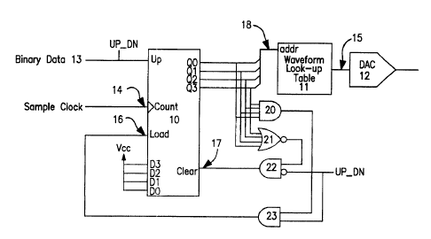
Fig. 1 of the drawings illustrates a first embodiment of the present
invention. The invention includes a binary input signal 13 to the direction
input of
a 4-bit up/down counter 10. The binary input signal will typically be received
from
a connection between an outside circuit or component and counter 10.
Up/down counter 10 in the embodiment of Fig. 1 also includes a count
input 14 operatively connected to a sample clock signal. Similar to the binary
input signal, the sample clock signal will typically be received from a
connection
between an outside circuit or component to counter 10. To ensure stable
circuitry timing, the sample clock frequency will normally be an integer
multiple of
the binary input data rate. The sample clock frequency also determines the
sample rate of the digitized output signal 15.
The normal operation of counter 10 in the preferred embodiment is such
that it changes its stored state at each rising edge of the sample clock
signal. If
the direction input is in a logic high state when the count input is
triggered, the
stored state of the counter increases by one. If the direction input is in a
logic
low state when the count input is triggered, the stored state of the counter
decreases by one.
CA 02279680 1999-08-OS
Counter 10 also includes load and clear inputs, 16 and 17. When the load
input of counter 10 is in a logic high state, the internal state of the
counter is set
to the values appearing at inputs DO-D3. When the clear input is in a logic
high
state, the internal state of the counter is set to all zeros.
The internal state of counter 10 is output on lines QO-Q3. These outputs
are operatively connected to the address line inputs 18 of waveform lookup
table
11. Lookup table 11 contains predetermined values stored at various addresses.
In a preferred embodiment, the values stored in lookup table 11 when taken
sequentially in time in order of increasing address, form a signal
representing the
output of a Gaussian filter following a positive-going step function input.
However, other predetermined values may be substituted as desired in a
particular application of the invention. The output 15 of lookup table 11 is
the
digital value corresponding to the contents of the address location specified
by
the address line inputs.
The output 15 of lookup table 11 can be optionally connected to digital-to-
analog converter circuit 12 if a shaped signal is desired in the analog
domain.
The design of the digital-to-analog converter circuit 12 will depend on the
details
of the design implementation, such as data rate or performance requirements,
as
is well known in the art.
Logic gates 20 and 23 serve to ensure that when the counter is in its
maximum state and the direction input indicates upward counting, the counter
remains in its maximum state. Counter output lines QO-Q3 comprise the four
inputs to AND gate 20. Consequently, when the counter is in its maximum state,
CA 02279680 1999-08-OS
lines QO-Q3 are high, and the output of AND gate 20 is also high. The output
of
AND gate 20 and the direction input line of counter 10 comprise the two inputs
of
AND gate 23. When both of these inputs are high, the output of AND gate 23 is
high, which is connected to the load input of counter 10. When the counter 10
load input is high, the state of counter 10 is set to the state of inputs DO-
D3,
which in this embodiment are all pulled high, and counter 10 is maintained in
its
maximum state in which all four bits are high.
Logic gates 21 and 22 serve to ensure that when counter 10 is in its
minimum state and the direction input indicates downward counting, the counter
remains in its minimum state. Counter output lines QO-Q3 comprise the four
inputs to NOR gate 21. Consequently, when the counter is in its minimum state,
and lines QO-Q3 are all low, the output of NOR gate 21 is high. The output of
NOR gate 21 and the inverted direction input line of counter 10 comprise the
two
inputs of AND gate 22. The output of AND gate 22 is connected to the clear
input of counter 10. Consequently, when AND gate 22 goes high, the counter
state is cleared and reset to all zeros, and counter 10 is maintained in its
minimum state.
The resulting operation of the embodiment depicted in Fig. 1 is
demonstrated by the example graphs of Fig. 2. In the example of Fig. 2,
counter
begins in a cleared zero state. As illustrated, the first bit of the binary
input
data is a logic high. Consequently, as the sample clock signal triggers the
count
input of counter 10, the direction input is logic high. The counter begins
incrementing its state, and sequentially addressing values in lookup table 11.
9
CA 02279680 1999-08-OS
Partway through segment B illustrated in the graph of the lookup table output,
the
counter reaches its maximum value. Thereafter, while the binary data input
remains logic high, logic gates 20 and 23 operate to cause counter 10 to
continuously reload its maximum state, thereby freezing the counter output and
consequently the lookup table address, ensuring a constant lookup table 11
output. When the binary data input is switched to a low logic level, the
apparatus
operates similarly but in reverse. Counter 10 decrements its state upon each
triggering of the count input by the sample clock signal, sequentially lower
addresses are addressed in lookup table 11, and the output decreases
progressively, as depicted in segment C of Fig. 2. If the counter reaches its
minimum state and the binary data input remains low, logic gates 21 and 22
operate to maintain the counter in its minimum state as previously explained.
While Fig. 1 depicts a preferred embodiment of the invention, it is
envisioned that somewhat varying circuit designs can be used to apply the
invention, without departing from its scope. For instance, different types of
up/down counters could be implemented in the invention. Furthermore, the
number of counter bits and the predetermined floor and ceiling counter states
could be varied as desired by one of ordinary skill in the art.
The embodiment of Fig. 3 depicts an additional feature of the invention.
Its operation will be described to the extent that it varies from that of Fig.
1. The
embodiment of Fig. 3 includes a means for providing an enable signal 33,
whereby the apparatus can be alternatively placed into an activated or
deactivated state. The means for providing an enable signal 33 will commonly
CA 02279680 1999-08-OS
comprise a connection from another circuit that is designed to control the
activation of the apparatus.
The enable signal 33 is connected to an inverting input of logic OR gate
46, and 2:1 multiplexer 45. When the enable signal is placed in its activated
state, which in the embodiment illustrated corresponds to a logic high level,
logic
OR gate 46 is unaffected, and a logic high signal originating from AND gate 44
will pass through OR gate 46 to the load input of counter 30 when the counter
reaches its maximum limit, as determined by AND gates 41 and 44 analogous to
the embodiment of Fig. 1. When a load signal is applied to counter 30 while
the
enable signal remains activated, the enable signal selects a first input of
multiplexer 45, which is tied to a logic high level, thereby applying the
desired
maximum state to counter 30 inputs DO-D3.
When the enable signal is placed in its inactivated state, which in this
embodiment is a logic low level, the output of OR gate 46 necessarily goes
high
and counter 30 will be forced into a loading condition. The enable signal also
selects the second input of multiplexer 45, which is tied to a logic low
level,
thereby applying a desired fixed state to counter 30 inputs DO-D3 to be loaded
while the apparatus is held inactive. In this embodiment, the state loaded
while
the appatatus is inactive corresponds to a halfway point between the counter's
minimum and maximum states, thereby allowing the apparatus output to rapidly
achieve its correct steady-state position upon its subsequent enabling,
regardless of the input state at the time of enabling. In many applications it
is
desirable to change from an activated to a deactivated state only while the
CA 02279680 1999-08-OS
counter occupies the desired steady-state value during normal operation.
Deactivating the device while the counter occupies other values can cause
significant discontinuities in the output signal, as the counter jumps to the
steady-
state value. In the aforementioned wireless radio transmitter context, as an
example, such discontinuities may generate unacceptable frequency content in
the transmitted signal.
While not essential to the operation of the invention, Figure 3 also depicts
flip flop 40. Flip flop 40 is provided in the illustrated embodiment to adjust
the
timing between the invention input signal and output signal, while also acting
as
an input buffer.
The foregoing description and drawings merely explain and illustrate the
invention and the invention is not limited thereto except insofar as the
appended
claims are so limited, inasmuch as those skilled in the art, having the
present
disclosure before them will be able to make modifications and variations
therein
without departing from the scope of the invention.
12