Note: Descriptions are shown in the official language in which they were submitted.
CA 02280024 1999-08-06
WO 98/35378 PCT/SE98/00210
1
MANUFACTURING A HETEROBIPOLAR TRANSISTOR AND A LASER DIODE
ON THE SAME SUBSTRATE
TECHNICAL FIELD
The present invention relates to manufacturing a heterobipolar transistor arid
a laser
s diode on or from the same substrate and it also relates to substrates
suitable for such
manufacturing.
BACKGROUND OF THE INVENTION
The research in the field of monolithic (i.e. arranged on or in the same chip
or circuit
plate) optoelectronic integrated circuits (OEICs) started in the end of the
seventies at
,o CALTECH, USA, see the article by C.P. Lee, S. Margalit, I. Ury and A.
Yariv,
"Integration of an injection laser with a Gunn oscillator on a semi-insulating
GaAs sub-
strate", Appl. Phys. Lett., Vol. 32, No. 12., pp. 806 - 807, June 1978. The
reason
thereof was the same as in developing electrical integrated silicon circuits,
i.e. it is de-
sired to manufacture both optical components such as lasers, waveguides,
detectors on
,s the same substrate as transistors, so that it could be possible to produce
chips in large
volumes and at low costs. Monolithic integration also reduces the number of
chips
what allows that more functionality can be packed into a circuit board, on
which
different chips are conventionally mounted. It can also increase the
reliability of a
system since fewer external connections are required. It should be added here
that a
2o condition for achieving these advantages is that the performance of the
various com-
ponents is not degraded when being integrated, compared to the case where they
are
manufactured separately.
The interest of finding a good solution to the problem how to combine optical
and
electronic components on the same chip nowadays emanates not only from the
tech-
Zs nical side but also from the system side. In order to be able to build the
optical net-
works of tomorrow, e.g. extending even into homes, less costly solutions are
required,
what in turn poses large demands on the technical development.
STATE OF THE ART
A large number of different alternative ways exist of achieving monolithic
integration.
3o It depends partly on the choice of wavelength and thereby the semiconductor
base
material which is to be used, such as whether to select either gallium
arsenide or
indium phosphide, and the choice of electric components such as whether a
hetero
bipolar transistor (HBT) or a field effect transistor (FET) is to be used, and
further the
choice of optical component, which is desired, such as a photodetector, laser
or
as modulator, partly also on the way in which the very integration is made. It
is common
to divide the methods used for integration in three classes:
CA 02280024 1999-08-06
WO 9$/35378 PCT/SE98/00210
2
- 1. Vertical integration. Two or more structures each including an electrical
or
optoelectrical component are formed sequentially on top of each other.
- 2. Horizontal integration. Two or more structures each including a component
are
formed side by side. First the different layers are formed for producing a
component
s and then these are etched away on selected portions of the chip at the side
of the
manufactured component. The next component is then grown on areas at which
material has been etched away.
- 3. Using the same basic structure for the two components. A basic layer
structure is
formed, which by further processing including for example etching for defining
,o individual components and only including applying layers for electrical
contacts but no
other layers results in components of various kinds isolated from each other.
The methods 1. and 2. have the advantage that in principle the individual
manufactured
components can be optimized. The disadvantage is that the methods of
manufacture
often will be very complex including a very large number of processing steps.
The
,s method 3. results in a simpler manufacturing process but also, most often a
com-
promise must be made as to the performance of the different components to be
manufactured.
A method which has often been mentioned in the literature is, to pass, for the
laser,
from vertical injection to lateral injection and such a laser is called an LCI-
laser
Zo ("Lateral Current Injection Laser"). Then the different n- and p-doped
layers are
defined by means of diffusion or implantation, which is made selectively on
different
portions of a substrate surface, and thereby both lasers and transistors can
be produced
from the same substrate or chip. This method has been used for integrating a
laser and
a FET, see the above cited article by C . P . Lee et al . , and of a laser and
HBT, see N .
is Bar-Chaim, Ch. Harder, J. Katz, S. Margalit, A. Yariv, I. Ury, "Monolithic
integration of a GaAiAs buried-heterostructure laser and a bipolar
phototransistor" ,
Appl. Phys. Lett., 40(7), 556, (1982). A disadvantage of this method is
however that
the result is a new type of laser and/or transistor. Another concept, which
has been
used, see T. Fukuzawa, M. Nakamura, M. Hirao, T. Kuroda, and J. Umeda, "Mono-
~o lithic integration of a GaAIAs injection laser with a Schottky-gate field
effect
transistor", Appl. Phys. Lett., 36(3), 181, (1980), is to first grow the laser
structure
and on top thereof an undoped layer, from which a FET can be produced. In
order to
obtain electrical contact with the top p-layer of the laser one then diffuses
a p-doping
(in this case zinc) through the undoped layer.
35 SUMMARY OF THE INVENTION
It is an object of the invention to provide a method, by means of which it is
possible to
,.. ~_ _..~. J
CA 02280024 1999-08-06
WO 98/35378 PCT/SE98/00210
3
manufacture in a simple way transistors and lasers on the same substrate or
chip
without degrading the performance of transistors and lasers owing to the
common
method of manufacture.
Thus, the problem solved by the invention is how to manufacture transistors
and lasers
s on the same substrate or chip, so that the performance of the transistors
and lasers thus
manufactured is substantially equal to that of separately fabricated
corresponding
components.
When manufacturing transistors and lasers on the same substrate a basic
structure is
first produced, which has a suitably selected sequence of semiconducting
layers
,o arranged on top of each other and in particular the start is a
substantially
"conventional" HBT-structure. The basic structure is then converted to a laser
on some
areas of the chip. The laser will thereby be the type vertical injection and
will thereby
be capable of obtaining the same performance as discrete lasers. The
conversion to a
laser structure is made by diffusing zinc into the material. The advantage
therein is
,s that one obtains substantially the same structure of the laser and HBT, as
if they had
been individually optimized. Similar structures have been made in GaAs/GaAIAs,
see
J. Katz, N. Bar-Chaim, P.C. Chen, S. Margalit, I. Ury, D. Wilt, M. Yust, A.
Yariv,
"A monolithic integration of GaAs/GaAIAs bipolar transistor and
heterostructure
laser", Appl. Phys. Lett., 37(2), 211, 1980. The method proposed in that paper
Zo includes that the active area of the laser is located in the base of the
HBT what is a
difference compared to the method as proposed herein. In the article A.K.
Goyal,
M.S. Miller, S.I. Long and D. Leonard, "A single epitaxial structure for the
integration of lasers with HBTs", SPIE, Vol. 2148, pp. 359 - 366, 1994, also
monolithic integration in the system GaAs/GaAIAs is used but the active region
is
is instead located in the collector in the same way as in the design described
herein, what
gives a larger freedom when designing the components and what allows an
individual
optimization of the two components to be made.
A heterobipolar transistor HBT and a laser diode LD are manufactured from a
common epitaxial structure. The transistor is then made directly from this
epitaxial
3o structure by only confining, separating, isolating and/or defining it by
etching and
applying electrical contact layers. The different active layers of the
transistor are thus
the epitaxial layers formed in the structure. In order to manufacture the
laser diode the
structure is changed by diffusing zinc into it, so that the topmost material
layers
change their types of doping from n-type to p-type. This is made in selected
areas of a
35 wafer, so that transistors and laser diodes in that way are monolithically
integrated.
Generally, the opposite change, i.e. from p-doping to n-doping in the upper
layers,
CA 02280024 1999-08-06
WO 98/35378 PCT/SE98/00210
4
could also be used.
Additional objects and advantages of the invention will be set forth in the
description
which follows, and in part will be obvious from the description, or may be
learned by
practice of the invention. The objects and advantages of the invention may be
realized
s and obtained by means of the methods, processes, instrumentalities and
combinations
particularly pointed out in the appended claims.
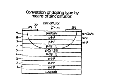
BRIEF DESCRIPTION OF THE DRAWINGS
A complete understanding of the invention and of the above and other features
thereof
may be gained from a consideration of the following detailed description of
non
,o limiting embodiments presented hereinbelow with reference to the
accompanying
drawings, in which:
- Fig. I is a schematic sectional view of a basic sequence of layers arranged
on top of
each other and suitable for producing a transistor,
- Fig. 2 is a sectional view of the sequence in Fig. 1, which illustrates
diffusion of
,s some substance into it in order to produce a structure suitable for a
laser,
- Fig. 3 is a schematic sectional view of a transistor manufactured from the
sequence
of layers in Fig. 1,
- Fig. 4 is a schematic sectional view of a laser manufactured from the basic
sequence
of layers in Fig. 1 modified according to Fig. 2,
zo - Fig. 5 is a diagram of Zn-concentration as a function of depth beneath
the surface of
the diffusion according to Fig. 2,
- Fig. 6 is a band diagram of the transistor according to Fig. 3 when being in
balance,
- Fig. 7 is a band diagram of a forwardly biased laser according to Fig. 4,
- Fig. 8 is a diagram of the measured voltage current ICE between collector
and
is emitter of the transistor according to Fig. 3 connected in a common emitter-
coupler
circuit as a function of the voltage VCE between the collector and the
emitter, and
- Fig. 9 is a diagram of the light power provided by the laser according to
Fig. 4 as a
function of the electric current.
DESCRIPTION OF THE PREFERRED EMBODIMENTS
3o In the following a description will be given of a specific embodiment using
specific
materials. It is to be understood that other materials having corresponding
properties
could also be used and in particular the specific doping types could be
changed to the
opposite doping types, i.e. n- and p-dopings could be replaced by p- and n-
dopings
respectively.
3s In Fig. ~ 1 a schematic sectional view of a common epitaxial sequence of
layers is
T __ __. _. ..__ ~. ~ ..
CA 02280024 1999-08-06
WO 98/35378 PCT/SE98/00210
shown which is suited for manufacturing HBTs and laser diodes on the same
substrate
and which is implemented in a material system based on indium phosphide InP.
For
simplicity all layers are there illustrated to have the same thickness,
whereas when
actually producing the structure naturally the layers have different
thicknesses
s depending on their intended operation, material, doping, etc. The epitaxial
structure is
grown by means of metalorganic vapor phase epitaxy MOVPE or by means of some
similar method, by means of which a good control both of layer thicknesses and
levels
of doping can be obtained. The substrate can be n-InP but it can be more
advantageous
to use semi-isolating, such as iron doped, InP in order to facilitate
monolithic
,o integration of a plurality of transistors and laser diodes, i.e. that a
plurality of
structures, which operates as transistors or laser diodes can be fabricated on
the same
chip. The epitaxial structure consists of a number of layers of varying
materials,
thicknesses and dopings which are p-type or n-type. Generally a material is
required
having a relatively wide band gap, here InP, a material having a narrower band
gap
,s and a higher refractive index, here InGaAsP, having a photoluminescence
wavelength
~pL = 1.3 ~m and called in short Q( i .3), and an optically active material,
here
InGaAsP, having a photoluminescence wavelength ~pL = 1.55 ~,m and called Q(
1.55)
in short. Moreover, a material having a relatively small band gap can be used
for
reducing contact resistances, here InGaAs.
zo The structure consists of, see Fig. 1,
- a buffer layer 1 of n-InP,
- a highly doped n-InP-layer 2,
- a weakly doped n-InP-layer 3,
- a weakly doped n-Q(1.3) layer 4,
is - un undoped multiple quantum well 5 comprising one or more strained or
unstrained
quantum wells surrounded by strained or unstrained barriers. The multiple
quantum
well 5 comprises thus in the preferred case a plurality of relatively thin
layers being
alternatingly two different types. The whole multiple quantum well is designed
to have
a net voltage equal to zero, i.e. it is voltage compensated,
30 - a highly doped p-Q(1.3) layer 6,
- a weakly doped n-InP layer 7,
- a highly doped n-InP layer 8 and
- at the top a highly doped n-InGaAs layer 9.
The layers 3, 4 and 5 form the collector and the layer 6 the base in the HBT
to be
as manufactured. The heterojunctions exist between the layers 3 and 4 and
between the
layers 6 and 7. In the laser to be produced the layer 5 forms the active
region and the
layer 4 and 6 the waveguide portion.
CA 02280024 1999-08-06
WO 98/35378 PCT/SE98/00210
6
After producing the epitaxial structure a diffusion processing step is
performed for
manufacturing a laser diode, see Fig. 2, in which zinc obtained from diethyl
zinc
(DEZn) in a gaseous shape, or from some other suitable zinc source, is
diffused into
the material, compare the arrow 21, at a temperature, a pressure and during a
time pe-
s riod, which result in a diffusion depth corresponding to at least the layers
7, 8 and 9 in
Fig. i . At those places where zinc has penetrated into the material, it is
incorporated
in the structure of the material and operates as an acceptor of electrons. For
a suitable
concentration it will compensate the n-doping in the top layers and an even
higher con-
centration of zinc results in that the material in these layers will be p-
doped. In order
,o to select areas on the wafer, in which the diffusion is to be made, the
whole wafer is
covered with silicon nitride SiN, see the layer 22, and areas in this layer
are opened
within intended regions by means of lithography in which thus SiN is removed.
The
areas covered by SiN then remains uninfluenced by the diffusion of zinc, see
Fig. 2.
Then is produced, by a combination of dry etching and wet etching of areas
selected
,s by means of lithography, a separation or confinement of the structures,
which are to
operate as HBTs, and those which are to form laser diodes, by producing
grooves
down to the substrate.
As has appeared above, the HBT is obtained directly by defining laterally the
sequence
of layers according to Fig. 1. The HBT has a vertical design and has contacts
to the
2o collector, the base and the emitter at the respective layer, see Fig. 3. It
is confined
laterally by a groove having two intermediate steps, one step at the top
surface of the
layer 2 and one step at the top surface of the layer 6. At these steps the
collector
contact 12 and the base contact 11 respectively are deposited. The groove
which is
located outside the collector contact 12 will, as has been indicated above
when
is referring to a confinement laterally of structures, extend into the
substrate. The
collector contact 12 could for an n-InP-substrate also possibly be located on
the under
side of the substrate. The emitter contact 13 is located on the exterior
surface of the
topmost layer. The functions of the different layers are
- the layer 2 works as a collector contact layer,
~o - the collector is formed by the layers 3 - 5,
- the layer 6 is the base of the transistor,
- the emitter is formed by the layer 7,
- the layers 8 and 9 are contact layers.
The feature distinguishing this structure from a conventional HBT is that the
band gap
3s of the material in the base must be sufficiently large in order not to
absorb the light
which is emitted from the quantum wells of the laser, in the case where the
structure is
T .~... 1
CA 02280024 1999-08-06
WO 98/35378 PCT/SE98/00210
7
modified to a laser. This results in that the band gap discontinuity in the
valence band
between the base and the emitter is reduced. However, it should be added, that
one
still has a sufficiently high discontinuity, in order not to appreciably
affect the current
gain of the transistor. A further difference is the existence of a multiple
quantum well
s located in the collector. However, this fact does not influence noticeably
the
characteristics (non-DC) of the transistor. No apparent differences exist in
the
operation of a component designed in the way described above, and a
conventional
HBT of high performance type.
The structure, which is produced by means of the diffusion process described
with
,o reference to Fig. 2, results after lateral definition and producing
contacting means in a
laser diode. A laser diode has an n-contact, which in the case where the
substrate is
semi-isolating, is identical to and located on the same surface as the
collector contact
i 2. If the substrate is n-InP the contact can be deposited on the under side
of the sub-
strate, as is illustrated at 14 in Fig. 4. The laser has a p-contact 15 on top
of the top-
s most layer 9 in the sequence of layers. The operation of the different
layers is then,
see Fig. 4:
- the layers 1 - 3 constitute the cladding and contact layers,
- a lower separate confinement heterostructure ("separate confinement
structure") SCH
in the layer 4,
Zo - the layer 5 is the active region,
- an upper separate confinement structure SCH in the layer 6,
- the layers 7 and 8 form a cladding,
- the layer 9 is a contact layer.
This structure contains all those parts which a conventional quantum well
laser of
zs double heterostructure type is to have, and is substantially identical to
the standard
structures used for advanced lasers for the wavelength 1.55 ~cm. One
difference is the
high p-doping, which exists in the top layer of the upper heterostructure and
is
necessary for the HBT and which could result in degraded performance of the
laser.
However, for moderate doping levels satisfactorily good results have been
obtained
3o and simulations indicate that for an improved design of the structure the
level can be
even more increased. In the separate heterostructures in the layers 4 and 6
the
heterojunctions of the corresponding transistor are located. Both the active
region of
the laser in the region 5 and the lower n-SCH in the layer 4 are located in
the collector
region of the corresponding transistor. The layer 6, which forms the upper p-
SCH,
as constitutes the base in the corresponding transistor.
In a practical experiment the epitaxial base structure illustrated in Fig. 1
was produced
u..WH..,.-.~.~.~~.-..~_.. ..~..,~.,~_.-_ .~~.,.~_...,
CA 02280024 1999-08-06
WO 98/35378 PCT/SE98/OOZ10
g
by means of metalorganic vapor phase epitaxy MOVPE of low pressure type at
680°C
on an n-InP-substrate. Zinc was diffused into the material using DEZn as a
source and
for an overatmospheric pressure of phosphine PH3 and using hydrogen gas as a
carrier
gas. The temperature was maintained at 475°C and the overatmospheric
pressure was
s 100 mbar during 1 h 20 min. A zinc concentration in the InP-layers exceeding
1 ~ 1018
was obtained, see the diagram in Fig. 5. The configuration of the produced
structures
appears from the tables below.
For manufacturing an HBT an emitter contact of Ti/Pt/Au was deposited by
evaporation and lift-off of photoresist layer and the metal layer deposited on
top
,o thereof in the conventional way and the remaining metal was then used as a
mask in
etching down to the base layer 6 by means of reactive ion etching (RIE) in a
plasma
including hydrogen gas and methane followed by a selective wet etching based
on
HC1:H20. Then a base contact of Pt/Ti/Pt/Au was applied in the same way as the
emitter contact. A silicon nitride mask was defined and covered the base and
the
,s emitter contacts. By means of dry etching portions of the base and
collector layers
were removed around the central structure for forming substantially structures
according to Fig. 3. The collector contact was deposited on the underside of
the
substrate by evaporating Ni/AuGe. In Fig. 8 the measured current ICE from
collector
to emitter is illustrated for the obtained transistor connected in a common
emitter
Zo circuit as a function of the voltage VCE between the collector and emitter
for the base
currents IB = 0, 20, 40, ..., 100 ~,A.
The manufacture of a laser diode of ridge type from the base structure started
by
patterning stripes having a width of 3 ~cm on the top surface in order to
confine the
laser structure and then a top contact was applied to the top surface in the
same way as
is the emitter contact above. The metal contact was then used as a mask in dry
etching
down to the p-cladding of the laser. Selective wet etching was used down to
the etch
stop layer in order to complete the ridge structure of the laser. For
passivating and
planarizing purposes then an 1.5 ~.m thick silicon nitride layer was deposited
by means
of PECVD (Plasma Enhanced Chemical Vapor Deposition, compare the passivating
~o regions 16 in Fig. 4). The wafer was polished down to a thickness of about
120 ~,m
and a bottom contact of AuGe/Ni/Ti/Pt/Au was applied by evaporation. The laser
was
then divided by splitting it and was mounted on a silicon carrier which served
as a heat
sink. In Fig. 9 a diagram of the light power provided by the manufactured
laser as a
function of injected current is illustrated.
T .~.., .r
CA 02280024 1999-08-06
WO 98/35378 PCT/SE98/00210
9
Table 1. HBT-structure
Layer Material Thickness Doping
[nm] [cm-3]
Contact InGaAs 50 n:5~
1018
s InP 1300 n:1~1018
InGaAsP (~=1,3~cm) 2 n: l
~ 1018
Emitter InP 200 n:5
~ 1
O 1
~
Distance
layer InGaAsP (~=1,3~m) 5 undoped
,o Base InGaAsP (~=1,3~um) 80 p:4~
1018
Collector 9xInGaAsP-(~=1,3~,m)-barrier layer,undoped
8
tensile stress 0,9 % ,
$xInGaAsP-(~=1,55~cm)-quantum well7 undoped
layer, compressive stress 1
,s Collector InGaAsP (~=1,3~cm) 40 n:l
~ 101
Collector InP 200 n: l
~ 101
Subcollector InP 500 n: l
~ 1018
Table 2. Laser diode structure
Layer Material Thickness
Doping
Zo [nm] [cm-3]
Contact InGaAs 50 p-cliff.
Cladding InP 1300 p-cliff.
Etch stop InGaAsP (~=1,3~m) 2 p-cliff.
1.
Cladding InP 200 p-cliff.
zs p-SCH InGaAsP (~=1,3~.m) 5 p-cliff.
p-SCH InGaAsP {~=1,3~cm) 80 p:4~1018
Active layer 9xInGaAsP-(~=1,3~m)-barner layer, 8 undoped
tensile stress 0,9 % ,
8xInGaAsP-(~=1,55~cm)-quantum well7 undoped
layer, compressive stress 1 %
n-SCH InGaAsP (~=1,3~cm) 40 n:1~101~
Cladding InP 200 n: l ~
101
Cladding InP 500 n: l ~
1018
CA 02280024 1999-08-06
WO 98/35378 PCTISE98100210
Calculated band diagrams of electrons/holes are illustrated in Figs. 6 and 7,
in which
Fig. 6 shows a band diagram of the HBT structure in a balanced state and Fig.
7
shows a band diagram of a laser diode structure being forwardly biased.
Above a laser structure of the edge-emitting type has been described. However,
it may
s also be advantageous to manufacture a surface-emitting laser, this requiring
only minor
modifications of some processing steps.
Additional advantages and modifications will readily occur to those skilled in
the art.
Therefore, the invention in its broader aspects is not limited to the specific
details,
representative devices and illustrated examples shown and described herein.
,o Accordingly, various modifications may be made without departing from the
spirit or
scope of the general inventive concept as defined by the appended claims and
their
equivalents.
~.